Article

Ga-Doped ZnO Coating—A Suitable Tool for Tuning the Electrode Properties in the Solar Cells with CdS/ZnS Core-Shell Quantum Dots

1
Department of Microelectronics, Technical University of Sofia, 1000 Sofia, Bulgaria
2
Central Laboratory of Solar Energy and New Energy Sources, Bulgarian Academy of Sciences, 1784 Sofia, Bulgaria
3
Institute of Optical Materials and Technologies, Bulgarian Academy of Sciences, 1113 Sofia, Bulgaria
4
Department of Chemistry, Government V.Y.T.PG. Autonomous College, Durg 491001, Chhattisgarh, India
5
Department of Physics, Dr. Harisingh Gour University, Sagar 470001, Madhya Pradesh, India
*
Author to whom correspondence should be addressed.
Crystals 2021, 11(2), 137; https://doi.org/10.3390/cryst11020137
Submission received: 4 January 2021 / Revised: 24 January 2021 / Accepted: 27 January 2021 / Published: 29 January 2021
(This article belongs to the Section Inorganic Crystalline Materials)

Abstract

:
Two layer system from sputtered indium tin oxide (ITO) and gallium doped zinc oxide (Ga:ZnO, GZO) were studied for transparency in the visible electromagnetic range, reflectivity in the near infrared range, conductivity and valent band for a solar cells with quantum dots. The bi-layer coatings produced at optimized oxygen partial pressure, films thickness and surface roughness exhibit improved optical properties without worsening the electrical parameters, even if additional oxygen introduction during the reactive sputtering of the GZO. With an average optical transmittance of 91.3% in the visible range, average reflection and resistivity lower than 0.4 × 10⁻² Ω.cm, these coatings are suitable for top electrode in the solar cells. The obtained results reveal that multilayered stacks of transparent ITO/Ga-doped ZnO coatings possess relatively low surface roughness (7–9 nm) and appropriate refractive index. The additional oxidation of GZO films induces modification of the film thickness and respectively of their optical performances.

Graphical Abstract

1. Introduction

Transparent conductive films are an important part of any optoelectronic device. Especially in the solar cell fabrication, the efficiency of the cell is strongly dependent on the quality of the transparent conductive electrode (TCE) [1,2]. It usually consists of oxide film (transparent conductive oxide (TCO)) or a system of few TCOs involving few interfaces. This electrode serves not only as an electrical conductor, but also as an optical filter. It is preferable if the TCE can transmit more than 82–85% of the visible light with broadband of the transmission characteristic (for efficient absorption of all wavelengths of the visible light from blue to red) and if it can reject the infrared (IR) and ultraviolet (UV) components [3]. UV light causes materials degradation, shortening the solar cells’ life and the IR heating component affects the charge carriers’ mobility in the films, which results in a throughput decrease.
According to available studies, approximately 30% of the total losses in the photoconductors are optical ones [4,5]. Therefore, these losses must be suppressed to a minimum, although no exact criterion exists about a satisfactory minimum. Optical losses reduction is especially crucial for the non-silicon, thin film perovskites cells, where the efficiency is naturally low and each percent of loss decrease is significant for the normal work of the cell. To improve the filtering quality of the TCE, the presence of single layer of indium-tin oxide (ITO) is not enough. At least few films with altering low and high refractive indexes have to be combined to achieve the desired transmission characteristic in the different wavelength ranges. The deposition method and the deposition conditions are extremely important for the performance of the TCE. Among the available methods for TCO deposition, such as chemical vapor deposition (CVD), spray pyrolysis, e-beam evaporation, atomic layer deposition (ALD), etc., the most applicable process remains the RF sputtering due to its flexibility in the tuning of the film’s properties with the process parameters [6,7,8]. As well, contamination with by-products and high temperature processing can be avoided, thus uncontrollable changes in the film’s properties are eliminated. By the main process’ parameters—sputtering voltage (power), sputtering pressure, deposition rate, and partial pressure of the reactive gas (degree of oxidation)—t is possible to control the main parameters of the TCO that are important for the solar cell work. Among them are the surface roughness, the film’s crystallinity [9], the film’s resistivity and its optical constants (the refractive index in the different wavelength ranges) [10]. The surface roughness is responsible for the losses caused by scattering of the rays from the peaks situated on the film’s surface and their distribution all over the film’s area. Additionally, the peaks may cause contact resistance increase, or even a breakthrough of the next deposited film. It is accepted that an average surface roughness of up to 5% on the total thickness of the film is satisfactory for the needs of TCE [11].
Researchers firstly have tried to replace the ITO with ZnO films, because of their thermal stability, non-toxicity and lower cost [12]. It has been fount suitable solution to solve the problem with the thermal instability of the ITO resistance. However, the absolute resistivity of ZnO is still too high as compared to the ITO. Metal dopants, such as Al, In or Ga, have been used to improve the electrical conductivity of the films [13,14,15]. After optimization of the doping concentration and film thickness Ga-doped ZnO (GZO) exhibited high thermal stability and comparable transparency to ITO, but they still had higher resistivity. Thus, the combination of GZO and ITO seems unavoidable. Reports already exist for the application of GZO/ITO bi-layer system in solar panels. The effect of the thickness and deposition temperatures on the microstructural and electrical properties of the sputtered GZO/ITO films has been studied [16]. The resistivity has been found to be dependent on the thickness ratio between the films and the post-deposition annealing. After optimization of both parameters, 85% transmittance in the visible range has been reported. Further, the internal stress of the GZO and ITO films and its effect on the visible transmission has been investigated as a function of the total sputtering pressure [17]. Recently, ZnO:Ga-graded ITO electrodes in perovskites solar cells have been reported [18]. Optical transmittance of 95%, resistivity of 2.3 × 10⁻⁴ Ohm cm, and work function of 4.23 eV have been reported after optimization of the power during DC co-sputtering. However, for an efficient solar cell, it is also necessary to achieve rejection of the IR spectrum (the heating component) in addition to the good transmittance in the visible region and the low resistance. To the authors’ knowledge similar study has not been carried out. According to the literature, the effect of the oxygen partial pressure during sputtering on the GZO film’s roughness and the complex optical characteristic, including visible and IR range, has not been yet investigated.
In this paper we tried to fill this gap by preparing GZO/ITO system. GZO films were deposited by RF sputtering at different oxygen pressures. The aim of the paper is to tune the surface roughness, sheet resistance and valence band of the bilayer coating, while keeping the transparency according to the current state-of-the-art (>90%). Additionally, it was observed suppression to some extend of the near infrared (NIR) and UV transmission, which is an extra advantage for the solar cell performance. Comparison of the produced films’ surface morphology, transmission spectra in the visible range, reflection spectra in the IR range, resistivity and the energy levels alignment was made with respect to the promising CdS/ZnS core-shell quantum dots based solar cell. Until now, the cells sensitized with quantum dots have used FTO (fluorine tin oxide) and ITO electrodes [19,20,21].

2. Materials and Methods

Thin films of ZnO doped by Ga (GZO), and ITO/GZO were prepared by RF sputtering of 3 inches-diameter targets positioned 6 cm above glass substrates. The substrates were preliminary cleaned according to the standard procedure by rinsing them in detergent solution of ammonia, hydrogen peroxide and distilled water in ratio 1:1:3. The sputtering voltage was kept constant for all sputtered combinations and it was 0.85 kV for the ITO films and 0.7 kV for the GZO films. The total sputtering pressure in the chamber (argon) was 1 × 10⁻³ Torr for the sample of single layer GZO and bi-layer ITO/GZO without additional oxidation. For the ITO/GZO1 the total sputtering pressure (argon + oxygen) was 1 × 10⁻² Torr due to introduction of oxygen, which corresponds to 10% oxidation. For ITO/GZO2 the total sputtering pressure (argon + oxygen) was 1 × 10⁻¹ Torr due to introduction of more oxygen, which corresponds to 20% oxidation. These relations were previously established and proved for the used vacuum installation (Leybold A400VL) in [22].
The thickness of the single GZO film was 100 nm. After insertion of the ITO the total thickness of the system before the additional oxidation was ~100 nm and the separated layers’ thicknesses were reduced to avoid optical parasitic effects. Further oxidation imposed to decrease the thickness of the GZO film to 40 nm and respectively to increase the thickness of the ITO film to 70 nm. For the highest oxidation degree, the thickness of the GZO was kept to 40 nm and the thickness of ITO was further increased to 85 nm. For simplicity, the following marking was introduced—GZO for sputtered GZO without additional oxidation; GZO1 for sputtered GZO and 10% additional oxidation; GZO2—for sputtered GZO and 20% additional oxidation. It means that in the sputtering chamber after setting the necessary sputtering argon pressure, the total pressure was increased by 10% and by 20% after adding oxygen as a reactive medium. It is determined by the mass flow controller and the vacuum meter as compared to the initial sputtering conditions, where no additional oxidation is initiated.
The oxygen content affects the optical parameters of the film because of the oxide film thickness and oxidation rate as a function of the oxygen gas pressure [23]. Then, in pair with ITO at some thickness combinations an unwanted effect of significant reflection in the visible range and small reflection in the NIR range was achieved (i.e., the coating absorbs the heat due to inappropriate thickness). This effect was eliminated by tuning the films thickness ratio. Preliminary simulations were conducted in the software environment of TFCalc to precisely determine the desired thickness. The error at the realization of the real thicknesses ratio is less than 1.3% and it is due to the films roughness. It served as a starting point. In addition, by decreasing the thickness of the GZO and increasing the oxygen content, its sheet resistance increased, therefore as a compensation effect the increase of the ITO thickness was necessary to prevent the electrode from electrical insulation and blocking the path of the current flow.
The refractive index and physical thickness, d, of the films were determined simultaneously from transmittance and reflectance spectra of the sample deposited on transparent substrates (optical glass) and the reflectance spectra of the corresponding films deposited on opaque Si substrates [24]. The previously developed three-step algorithm [25] was used for reliable isolation of physically correct solutions and for high accuracy determination, for instance, Δd = ±1 nm.
The films’ resistance was measured by by 4 point prober FPP-5000 Veeco. The optical transmittance in the UV and visible range was measured by UV-VIS Spectrophotometer NU-T6PC. The optical reflectance in the IR region was measured by Hitachi U-4100 near infrared spectrophotometer. The films thicknesses were determined from the cross-sectional view of the samples imaged by scanning electron microscope Philips 515. 3D topographies of the film surfaces were scanned by atomic force microscope (AFM) MFP-3D, Asylum Research, Oxford Instruments in non-contact mode. Ultraviolet photoelectron spectroscopy (UPS) was conducted with AXIS Supra, Kratos Analytical, UK (SHIMADZU group), having high photon flux He gas discharge lamp at 40.8 eV.

3. Results and Discussion

Figure 1a shows the refractive index of GZO layers as a function of the oxygen total sputtering pressure, changing due to additional oxygen flow introducing. It can be noted an increase of the refractive index from 1.72 without additional oxidation of the target, to 1.98 after 1 × 10⁻¹ Torr introduction of additional oxygen pressure. Figure 1b shows the variation of the refractive index in the range from UV to NIR for the three kinds of coatings oxidized at various extend and Figure 1c shows the refractive index of ITO only.
Possible reason for increasing of the refractive index with the oxidation degree could be the relation between the refractive index of a transparent oxide film and the inter-atomic separation, which is inversely proportional [27], and it can be also correlated to the film packing density. The films deposited without additional oxidation were characterized with the highest measured roughness, resulting in lower film density, which in turn resulted in the lowering of the refractive index. On additional oxidation, there is a reduction in the inter-atomic spacing and decreasing of the roughness, resulting in the densification of the films, leading to corresponding increase in the refractive index. Similar effects have been reported for HfO2 films [28] and MgTiO3 films produced by RF sputtering [29].
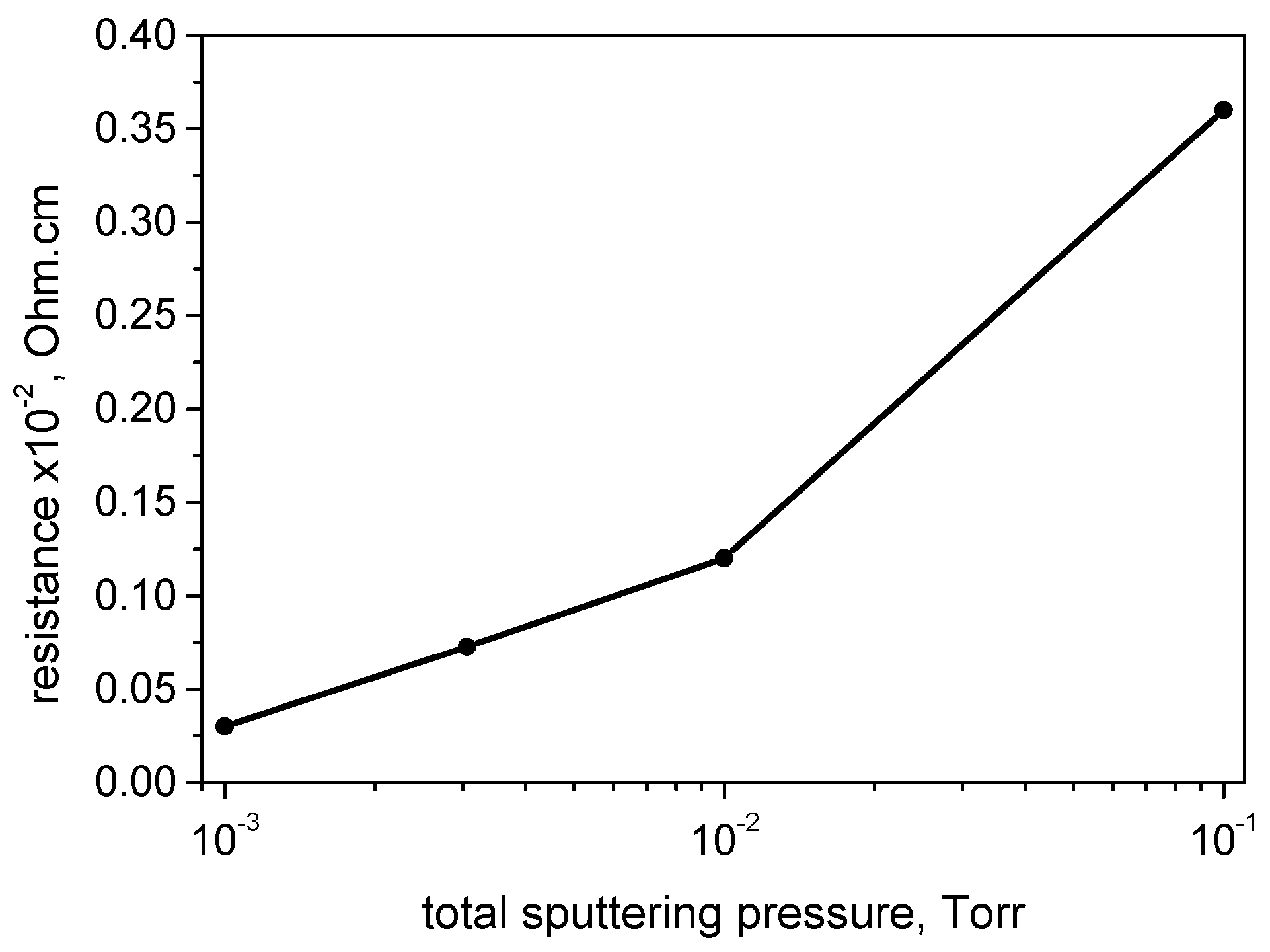
The GZO single layer deposited without additional oxidation of the target showed a resistivity of 1.67 × 10⁻² Ω.cm. Insertion of ITO resulted in a resistance decrease to 0.03 × 10⁻² Ω.cm. It is known that the electrical properties of the GZO films are improved by introducing ITO film [16]. However, due to the additional oxidation of GZO and the resulting increase of its electrical resistance, it is not possible to keep one and the same thickness for both films. The resistivity of the double ITO/GZO stack increased with increasing the oxygen amount during sputtering. However, due to the presence of ITO the variation of the resistance is not great—0.12 × 10⁻² Ω.cm at 10% oxidation and 0.36 × 10⁻² Ω.cm at 20% oxidation (Figure 2). Thus, an useful sputtering pressure window is provided for successful producing of TCE based on GZO. The trend in the resistance change can be ascribed to the oxygen that reduces the oxygen vacancy density in the film, resulting in free electrons trapping and the carriers’ concentration decreasing in the film [30].
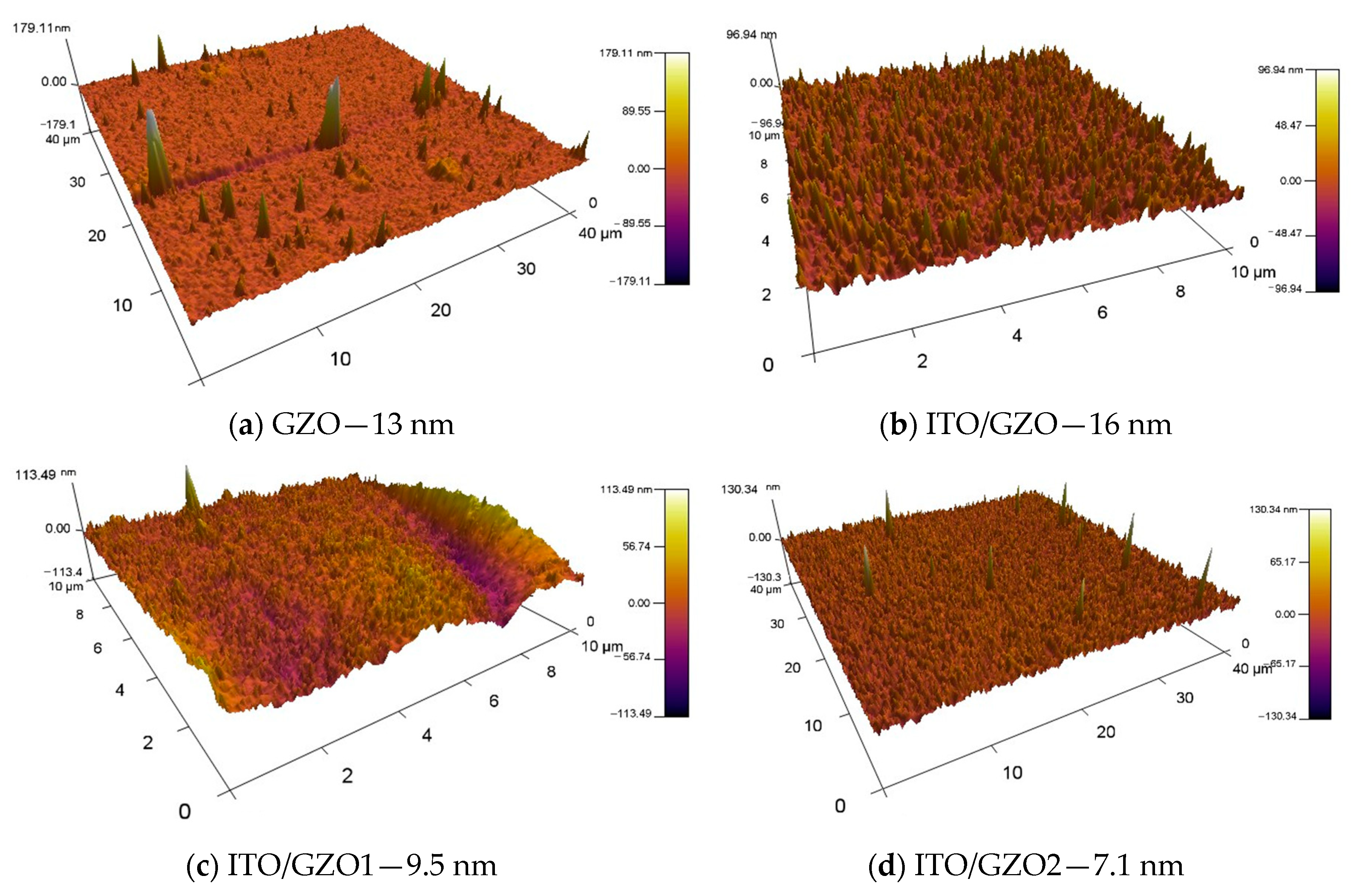
At the same time, it was found that the introduction of oxygen caused the surface roughness of the GZO film to decrease. Figure 3 showed comparison between the AFM images and average roughness of GZO single film, ITO/GZO bi-layer system without oxidation and ITO/GZO at additional oxidation of 10% and 20%.
According to the roughness data extraction, it could be compared that GZO film exhibited roughness of 13 nm and the insertion of ITO resulted in a slightly increase of the roughness to ~16 nm. Further, the GZO film growth with oxidation showed 9.5 nm and 7.1 nm roughness at 10% and 20% of oxidation, respectively. However, due to the resistance increase, it was necessary to increase the ITO film thickness for compensation, in order to keep the relation between the bi-layer system resistance and the films ratio [16]. Although great number of hills existed in Figure 3b as compared to Figure 3a they were more uniformly distributed and less sharp due to the ITO insertion. Further, the number and height of the sharp peaks decreased with the oxygen content increase during sputtering (Figure 3c,d). This might be due to the better crystallites arrangement because of the GZO films densification and voids filling [32]. Therefore, depending on the oxidizing conditions, the optimal film can be smooth on an atomic level.
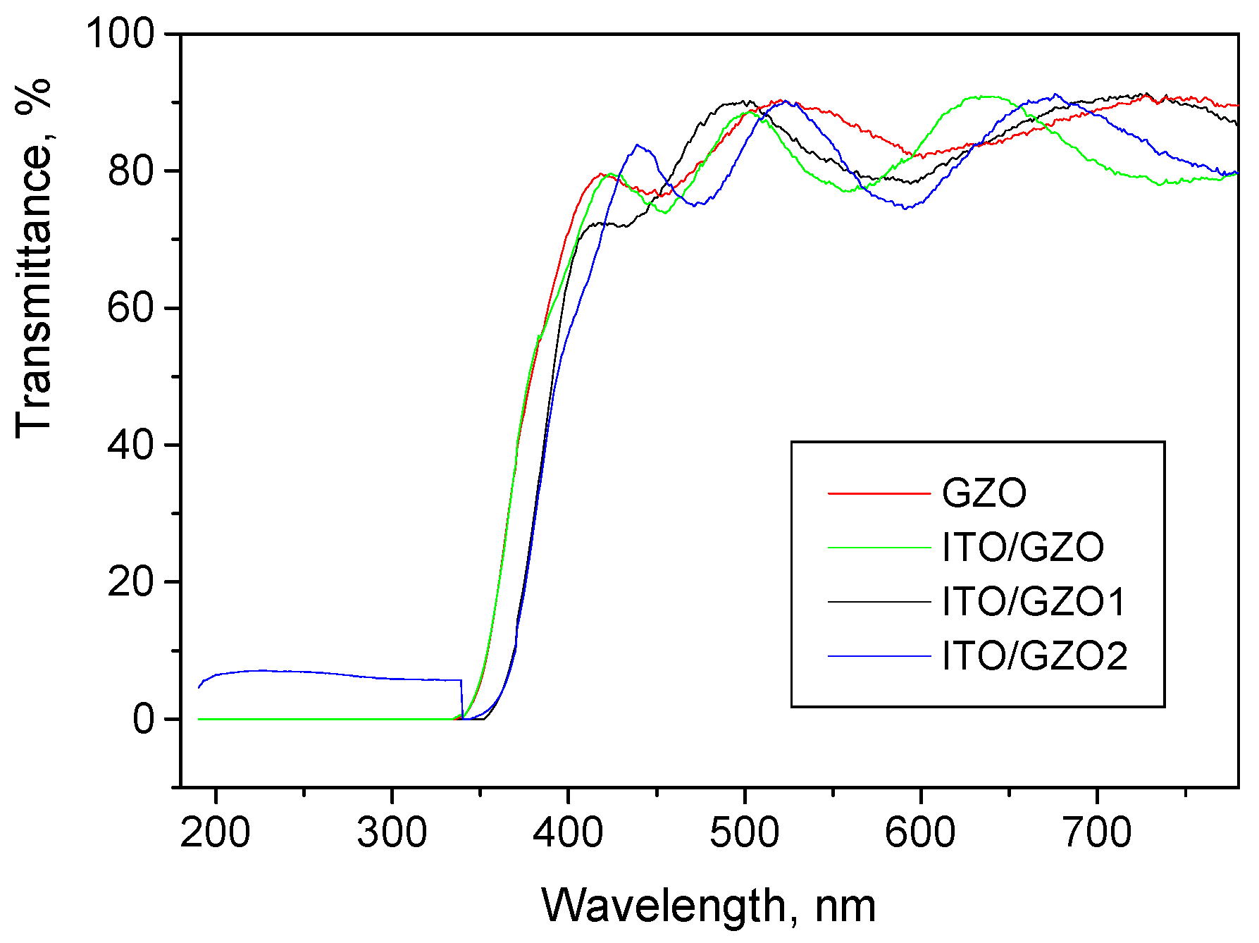
The smoother films are expected to result in the decrease of the optical losses during transmittance of the visible light. They also suggest greater contact area and lower contact resistance with the neighbor photoconductive film, which is significant for the smooth charge carriers’ extraction and electrical losses reduction. To investigate this relation, the transmission spectra in broad wavelength region between 190 nm and 800 nm were measured for each sample produced at specific oxygen pressure, in order to provide the trend in the transmittance as a function of the oxygen content and the results were shown in Figure 4. The measurement was conducted in a single beam mode with grating 1200 lines/mm with wavelength accuracy ± 0.5 nm and photometric accuracy ± 0.5% T (0–100% T), as well as consequent switching of deuterium lamp in the UV range and 50 W tungsten-halogen lamp in the visible and near infrared regions. It was found that the mean optical transmittance of the strongest oxidized film in the visible region was 91.3% and the transparency for the UV component was approximately 6%. For all GZO coatings the spectra in the near UV region (<400 nm) exhibited very sharp absorption edge.
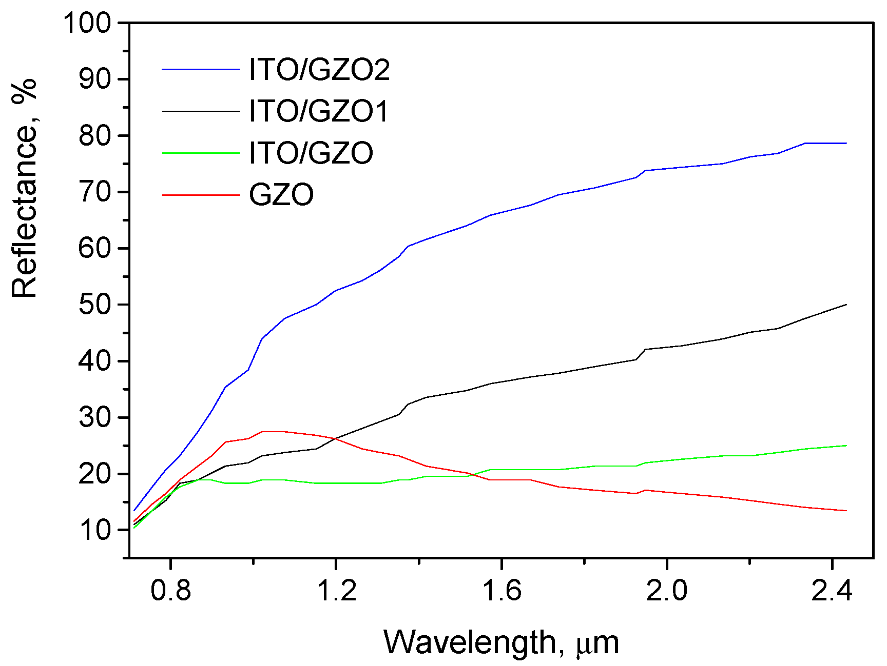
A slight shift of the optical interference maximums and minimums to the longer wavelengths is noted for the strongest oxidized film ITO/GZO2 as compared to the rest films. This is in consistent with the literature [33,34,35] and can be explained with the increased thickness, which is the greatest for this sample. Single layer of GZO showed 91% optical transparency (excluding the effect of glass substrate) in the same region and UV transmittance close to zero, however, its electrical resistance was not suitable for electrode purposes. Then insertion of ITO sublayer without additional oxidation of GZO during sputtering process resulted in slight worsening of the transmission spectrum in the visible range up to 90.9%. This can be probably due to light scattering as this determined to show greater surface roughness. Further increase of the oxygen pressure, induced an improvement of optical transparency to 91.2% and 91.3%. Although the difference in the spectra from the visible range is negligible, a significant difference could be noted in the infrared range (Figure 5), where the reflection of the near infrared (NIR) component is crucial for the efficiency of the solar cells.
The influence of the additional oxidizing is clear in the reflectance data in the NIR region. It can be seen that the single layer GZO and ITO/GZO without oxidation exhibited relatively low rejection ability of the IR component—the mean reflectance is 15–20%, which means that the transmission in the VIS and NIR ranges is almost the same (average ~85%).The increased refractive index of the GZO films during sputtering and the unchanged refractive index of the ITO films resulted in discrimination of the IR wavelengths transmission and optical (respectively heat) rejection greater than 65% for ITO/GZO2. The condition for altering films with high and low refractive indexes is not followed for the combination ITO/GZO2, which strongly narrowed the transmission band to the visible range [36].
Considering the Lorentz–Lorentz relationship [37] we can deduce sensitivity toward the film thickness variation due to the roughness variation from film to film produced at different oxidation degree by using the following relation (Equation (1)):
n 2 1 n 2 + 2 = 4 π 3 i N i α i ρ i μ i
where n is the refractive index, Ni is the number of i-th molecules per mol, αi is the i-th molecule polarizablity, ρi is the i-th molecule density and μi is the molecular weight of the i-th molecule.
The behavior of the of the system can be well explained with the following Equations (2) and (3) [38]:
R = r 1 2 + δ | t 1 r 2 t 2 | 2 1 δ 2 | r 2 | 4 ,
T = δ | t 1 t 2 | 2 1 δ 2 | r 2 | 4 ,
where r1 and t1 are the reflection and transmission coefficients for a beam passing through the by-layer coating from outside in; the r2 and t2 are for a beam passing through the coating from inside out; δ is absorption factor. They are function of the thickness, refractive index and extinction coefficient of the individual layers and could be determined by transfer matrix method [39].
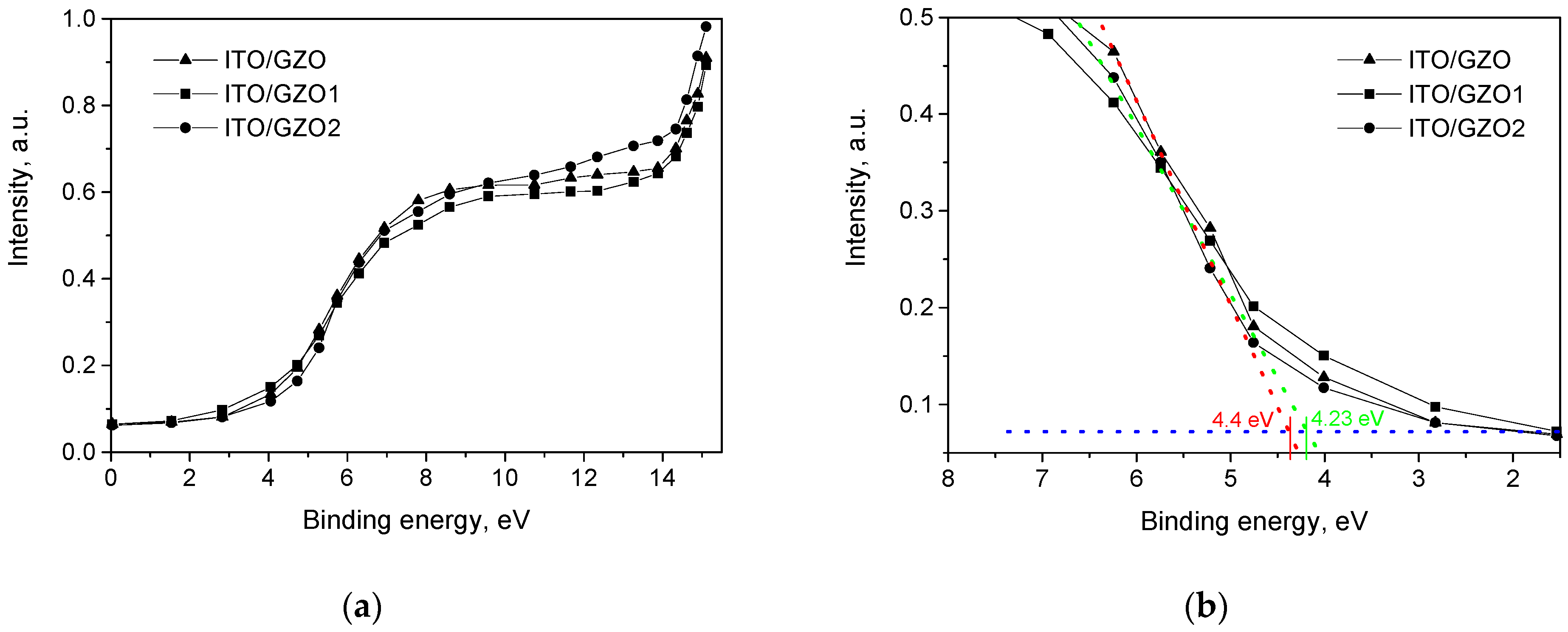
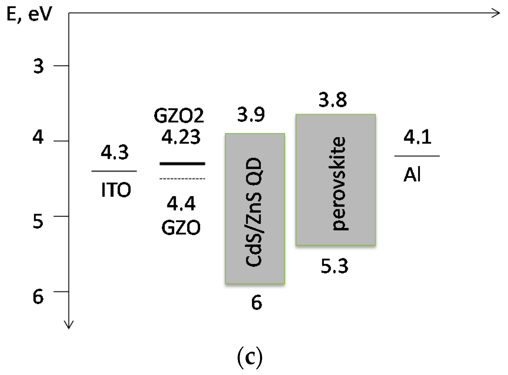
By using UPS technique, it was measured the work function of the ITO/GZO films at various oxidation degrees to investigate the band diagram and the energy level alignment with respect to perovskite solar cell with CdS/ZnS core-shell quantum dots based absorber (Figure 6a–c).
In this way the extraction ability at the interface can be estimated by the height of the energy barrier at the junctions. The methodology for determination of the GZO films’ work function is described elsewhere [40] and it relies on determination of the bandgap from the binding energy at the UPS spectrum edge and the photon energy . Initially, the work function of GZO was 4.4 eV, which is higher than those of ITO and caused stepping transport of the electrons to the ITO cathode. With an increase of the oxidation degree, the work function of GZO2 decreased to 4.23, thus forming breakdown of the interface barrier height between the CdS/ZnS core-shell quantum dots conduction band and ITO from 0.4 eV into two partitions—0.33 eV and 0.07 eV. Therefore, the solar cells involving this type of absorbers will have enhanced electrons extraction at the interface from the perovskite layer due to the favorable energy level alignment. This is expected to gain the throughput of the cell. The binding energy scale was referenced to the Fermi level. The position of the Fermi edge was set by using gold (Au) film electrically connected and positioned next to the tested GZO samples. The valence band maximum of GZO1 and GZO2 were determined by intersection between linear fitting to the background signal and the slope of the leading edge of the spectrum in the range 4–8 eV.
The studies of the optical coatings transmitting selectively the visible range of the electromagnetic waves spectrum and rejecting the outer neighboring bands by using conventional materials of silicon dioxide and titanium dioxide have shown that the most simple but still effective filters consist of at least 9 to 11 layers [41,42]. The total thickness of this multilayer stack is reported to be near 1 μm, which thickness is suitable for bulk solar cells. The optical losses due to the multiple interfaces creating conditions for multiple scattering because of the films roughness can reach 5% depending on the deposition method and mode. The electrical losses due to increased contact resistance due to the same reason (films roughness) can reach 7% [43]. Thus, the total losses are not acceptable for thin film solar cells. Moreover, the electrode coating in our work is intended for implementation in lead-free perovskite solar cells, which are theoretically less efficient. Therefore, the clear advantage of the proposed system of optical coatings is simple design giving satisfactory results for films roughness, transmission and reflection in all relevant ranges and suitable valence band level, paving the path toward optimization of the thin film lead-free perovskite solar cell modules.

4. Conclusions

ITO/GZO by-layered coatings were deposited on glass substrates by RF sputtering at various oxygen contents. The electrical and optical properties of the bi-layer system were strongly affected by the oxidation degree and the surface roughness of the GZO layer. The optical data showed that the additionally oxidized GZO films with ITO underlayer exhibited slightly differed mean visible transmittance over 90%, but the difference of the reflection spectra in the IR range is more significant –the films IR rejection ability differs with almost 40%. This behavior was attributed to the refractive index change for the GZO after oxidation, which in combination with the ITO resulted in a narrowing of the range for optical transmittance. GZO2 is characterized with a lower valence band energy than GZO and intermediate valence band energy between the CdS/ZnS core-shell quantum dots used in solar cells and the ITO film. This suggests facilitation of the electron extraction from the absorber to the cathode. In summary, ITO/GZO2 could serve as a transparent conductive electrode and partially as a heat mirror, or sunshade coating. Additionally, UV filtration is achieved, which is expected to slow down the aging processes in the cells. The future work will be related to impedance spectroscopic study for detailed estimation of the contact properties of solar cells implementing ITO/GZO as a front filtering electrode and determination of the electrical losses at the bi-layer coating’s interface.

Author Contributions

Conceptualization, M.A.; methodology, M.A.; validation, T.I., K.G. and A.K.S.; formal analysis, M.A., V.S., T.I., J.S.; investigation, M.A., V.S., T.T.; resources, M.A., A.K.S.; data curation, M.A., K.G.; writing—original draft preparation, M.A.; writing—review and editing, T.I.; visualization, V.S., T.T., M.A.; supervision, M.A., K.G.; project administration, M.A.; funding acquisition, M.A. All authors have read and agreed to the published version of the manuscript.

Funding

This research was funded by Bulgarian National Science Fund, grant number KP06-India-6 under the program for bilateral cooperation Bulgaria-India, call 2018.

Institutional Review Board Statement

Not applicable.

Informed Consent Statement

Informed consent was obtained from all subjects involved in the study.

Data Availability Statement

Data available on request due to privacy.

Conflicts of Interest

The authors declare no conflict of interest. The funders had no role in the design of the study; in the collection, analyses, or interpretation of data; in the writing of the manuscript, or in the decision to publish the results.

References

  1. Kumar, A. Predicting efficiency of solar cells based on transparent conducting electrodes. J. Appl. Phys. 2017, 121, 014502. [Google Scholar] [CrossRef]
  2. Lee, H.B.; Jin, W.-Y.; Ovhal, M.M.; Kumar, N.; Kang, J.-W. Flexible transparent conducting electrodes based on metal meshes for organic optoelectronic device applications: A review. J. Mater. Chem. C 2019, 7, 1087–1110. [Google Scholar] [CrossRef]
  3. Holman, Z.C.; Filipic, M.; Descoeudres, A.; Wolf, S.D.; Smole, F.; Topic, M.; Ballif, C. Infrared light management in high-efficiency silicon heterojunction and rear-passivated solar cells. J. Appl. Phys. 2013, 113, 013107. [Google Scholar] [CrossRef] [Green Version]
  4. Abdullah, M.F.; Alghoul, M.A.; Naser, H.; Asim, N.; Ahmadi, S.; Yatim, B.; Sopian, K. Research and development efforts on texturization to reduce the optical losses at front surface of silicon solar cell. Renew. Sustain. Energy Rev. 2016, 66, 380–398. [Google Scholar] [CrossRef]
  5. Fazal, E.; Khan, S.A.D.; Khan, A.D.; Ullah, N.; Imran, M.; Noman, M. Optical optimization of double-side-textured monolithic perovskite–silicon tandem solar cells for improved light management. RSC Adv. 2020, 10, 26631–26638. [Google Scholar]
  6. Navid, M.S.J.; Mahmoudysepehr, M.; Sivoththaman, S. Highly conductive TCO by RF sputtering of Al:ZnO for thin film photovoltaics. In Proceedings of the 42nd Photovoltaic Specialist Conference (PVSC), New Orleans, LA, USA, 14–19 June 2015. NSPEC Accession Number: 15664590. [Google Scholar]
  7. Misra, P.; Ganeshan, V.; Agrawal, N. Low temperature deposition of highly transparent and conducting Al-doped ZnO films by RF magnetron sputtering. J. Alloys Compd. 2017, 725, 60–68. [Google Scholar] [CrossRef]
  8. Das, R.; Das, H.S.; Nandi, P.K.; Biring, S. Comparative studies on the properties of magnetron sputtered transparent conductive oxide thin films for the application in solar cell. Appl. Phys. A 2018, 124, 631. [Google Scholar] [CrossRef]
  9. Ali, K.; Khan, S.A.; Jafri, M.Z.M. Structural and optical properties of ITO/TiO2 anti-reflective films for solar cell applications. Nanoscale Res. Lett. 2014, 9, 175. [Google Scholar] [CrossRef] [Green Version]
  10. Isiyaku, A.K.; Ali, A.H.; Nayan, N. Structural optical and electrical properties of a transparent conductive ITO/Al–Ag/ITO multilayer contact. Beilstein J. Nanotechnol. 2020, 11, 695–702. [Google Scholar] [CrossRef]
  11. Raoufi, D.; Hosseinpanahi, F. The effect of film thickness on surface morphology of ITO thin films. J. Theor. Appl. Phys. 2013, 7, 21. [Google Scholar]
  12. Ziemińska-Stolarska, A.; BareckaIreneusz, M.; Zbicinski, Z. Effect of replacement of tin doped indium oxide (ITO) by ZnO: Analysis of environmental impact categories. In Proceedings of the International Conference Energy, Environment and Material Systems (EEMS 2017), Polanica-Zdroj, Poland, 13–15 September 2017; Volume 19, p. 02026. [Google Scholar]
  13. Ponja, S.D.; Sathasivam, S.; Parkin, I.P.; Carmalt, C.J. Highly conductive and transparent gallium doped zinc oxide thin films via chemical vapor deposition. Sci. Rep. 2020, 10, 638. [Google Scholar] [CrossRef] [PubMed] [Green Version]
  14. Belkhaoui, C.; Mzabi, N.; Smaoui, H.; Daniel, P. Enhancing the structural, optical and electrical properties of ZnO nanopowders through (Al + Mn) doping. Res. Phys. 2019, 12, 1686–1696. [Google Scholar] [CrossRef]
  15. Ivanova, T.; Harizanova, A.; Koutzarova, T.; Vertruyen, B.; Closset, R. Structural and optical characterization of nitrogen and gallium co-doped ZnO thin films, deposited by sol-gel method. J. Mol. Struct. 2020, 1206, 127773. [Google Scholar] [CrossRef]
  16. Chung, A.; Cho, S.; Cheong, W.; Lee, G.H.; Kang, B.S.; Song, P. Investigation on the interface of GZO/ITO double-layered transparent conducting oxide films for solar cells. J. Ceram. Proc. Res. 2012, 13, s10–s15. [Google Scholar]
  17. Sasabayashi, T.; Song, P.K.; Shigesato, Y.; Utsumi, K.; Kaijo, A.; Mitsui, A. Internal Stress of ITO, IZO and GZO Films Deposited by RF and DC Magnetron Sputtering. MRS Online Proc. Libr. 2000, 666, 241–246. [Google Scholar] [CrossRef]
  18. Seok, H.-J.; Ali, A.; Seo, J.H.; Lee, H.H.; Jung, N.-E.; Yi, Y.; Kim, H.-K. ZnO: Ga-graded ITO electrodes to control interface between PCBM and ITO in planar perovskite solar cells. Sci. Technol. Adv. Mater. 2019, 20, 389–400. [Google Scholar] [CrossRef] [Green Version]
  19. Zavaraki, A.J.; Liu, Q.; Ågren, H. Solar cell sensitized with “green” InP-ZnS quantum dots: Effect of ZnS shell deposition. Nano-Struct. Nano-Objects 2020, 22, 100461. [Google Scholar] [CrossRef]
  20. Liu, L.; Li, H.; Liu, Z.; Xie, Y.-H. The conversion of CuInS2/ZnS core/shell structure from type I to quasi-type II and the shell thickness-dependent solar cell performance. J. Colloid Interface Sci. 2019, 54615, 276–284. [Google Scholar]
  21. Park, Y.J.; Lee, K.S.; Lim, G.H.; Seo, H.W.; Kim, S.W.; Kim, M.; Yi, Y.; Lee, H.S.; Son, D.I. Role of CdSe and CdSe@ZnS quantum dots interlayers conjugated in inverted polymer solar cells. Org. Electron. 2020, 82, 105707. [Google Scholar] [CrossRef]
  22. Dobrikov, G.; Rassovska, M.; Andreev, N.; Boyadzhiev, S.; Gesheva, K.; Ivanova, T.; Sharlandjiev, P.; Nazarova, D. Development of transparent heat mirrors based on metal oxide thin film structures. Thin Solid Films 2009, 518, 1091–1094. [Google Scholar] [CrossRef]
  23. Xu, Z.; Rosso, K.M.; Bruemmer, S. Metal Oxidation Kinetics and the Transition from Thin to Thick Films. Phys. Chem. Chem. Phys. 2012, 14, 14534–14539. [Google Scholar] [CrossRef] [PubMed] [Green Version]
  24. Konstantinov, I.; Babeva, T.; Kitova, S. Analysis of errors in thin-film optical parameters derived from spectrophotometric measurements at normal light incidence. Appl. Opt. 1998, 37, 4260–4267. [Google Scholar] [CrossRef] [PubMed]
  25. Babeva, T.; Kitova, S.; Konstantinov, I. Photometric methods for determining the optical constants and the thicknesses of thin absorbing films: Criteria for precise and unambiguous determination of n, k, and d in a wide spectral range. Appl. Opt. 2001, 40, 2682–2686. [Google Scholar] [CrossRef] [PubMed] [Green Version]
  26. Aleksandrova, M.; Dobrikov, G.; Gesheva, K.; Bodurov, G.; Cholakova, I.; Kolev, G. Deposition of Transparent Electrodes for the Future Generation of Flexible Displays. In Proceedings of the International Scientific Conference on Information, Communication and Energy Systems and Technologies ICEST, Veliko Tarnovo, Bulgaria, 28–30 June 2012. [Google Scholar]
  27. Li, P.; McDonald, J.F.; Lu, T.M. Densification induced dielectric properties change in amorphous BaTiO3 thin films. J. Appl. Phys. 1992, 71, 5596–5600. [Google Scholar] [CrossRef]
  28. Hu, H.; Zhu, C.X.; Lu, Y.F.; Liew, Y.; Li, M.F.; Cho, B.J.; Chio, W.K.; Yakovlev, N. Physical and electrical characterization of HfO2 metal-insulator-metal capacitors for Si analog circuit application. J. Appl. Phys. 2003, 94, 551–557. [Google Scholar] [CrossRef]
  29. Kumar, S.; Bhuyan, R.; Pamu, D. Effect of post annealing on structural, optical and dielectric properties of MgTiO3 thin films deposited by RF magnetron sputtering. Appl. Surf. Sci. 2013, 264, 184–190. [Google Scholar] [CrossRef]
  30. Zhao, J.L.; Sun, X.W.; Ryu, H.; Moon, Y.B. Thermally stable transparent conducting and highly infrared reflective Ga-doped ZnO thin films by metal organic chemical vapor deposition. Opt. Mat. 2011, 33, 768–772. [Google Scholar] [CrossRef]
  31. Aleksandrova, M.; Ivanova, T.; Gesheva, K.; Strijkova, V.; Tsanev, T.; Singh, J.; Singh, A.K. Fabrication of transparent ITO/Ga-doped ZnO coating as a front panel electrode toward efficient thin film solar cells. Mater. Proc. 2020, 2, 1. [Google Scholar] [CrossRef]
  32. Mo, G.; Liu, J.; Lin, G.; Zou, Z.; Wei, Z.; Liu, Y.; He, H.; Fu, Y.; Shen, X. Characterization of low resistivity Ga-doped ZnO thin films on Si substrates prepared by pulsed laser deposition. Mater. Res. Express 2019, 6, 106421. [Google Scholar] [CrossRef]
  33. Lansåker, P.C.; Petersson, P.; Niklasson, G.A.; Granqvist, C.G. Thin sputter deposited gold films on In2O3:Sn, SnO2:In, TiO2 and glass: Optical, electrical and structural effects. Sol. Energy Mater. Sol. Cells 2013, 117, 462–470. [Google Scholar] [CrossRef]
  34. Valluzzi, M.G.; Valluzzi, L.G.; Meyer, M.; Hernández-Fenollosa, M.A.; Damonte, L.C. Optical and Electrical Properties of TiO2/Co/TiO2 Multilayer Films Grown by DC Magnetron Sputtering. Adv. Cond. Matt. Phys. 2018, 2018, 1257543. [Google Scholar] [CrossRef] [Green Version]
  35. Subacius, A.; Baloukas, B.; Bousser, E.; Hinder, S.J.; Baker, M.A.; Rebholz, C.; Matthews, A. Nanostructural Characterisation and OpticalProperties of Sputter-Deposited Thick Indium TinOxide (ITO) Coatings. Coatings 2020, 10, 1127. [Google Scholar] [CrossRef]
  36. Kim, J.-H.; Fujita, S.; Shiratori, S. Design of a thin film for optical applications, consisting of high and low refractive index multilayers, fabricated by a layer-by-layer self-assembly method. Colloids Surf. A Physicochem. Eng. Asp. 2006, 284–285, 290–294. [Google Scholar] [CrossRef]
  37. Mada, Y.; Sugitani, S.; Arai, K.; Yamasaki, K. Optical properties of oxygen-ion-implanted benzocyclobutene films. J. Vac. Sci. Technol. A 2001, 19, 883–886. [Google Scholar] [CrossRef]
  38. Hinczewski, D.S.; Hinczewski, M.; Tepehan, F.Z.; Tepehan, G.G. Optical filters from SiO2 and TiO2 multi-layers using sol–gel spin coating method. Sol. Energy Mater. Sol. Cells 2005, 87, 181–196. [Google Scholar] [CrossRef]
  39. Pedrotti, F.L.; Pedrotti, L.S. Introduction to Optics; Prentice-Hall: London, UK, 1993; p. 392. [Google Scholar]
  40. Park, Y.; Choong, V.; Gao, Y. Work function of indium tin oxide transparent conductor measured by photoelectron spectroscopy. Appl. Phys. Lett. 1996, 68, 2699. [Google Scholar] [CrossRef]
  41. Macleod, H.A. Thin Film Optical Filters, 3rd ed.; The Institute of Physics: London, UK, 2001. [Google Scholar]
  42. Abdullah, G.H.; Mohammad, E.; Hadeeabud, A.M. Design and analysis narrowband filters, International. J. Photon. 2013, 5, 13–19. [Google Scholar]
  43. Dhankhar, M.; Singh, O.P.; Singh, V.N. Physical principles of losses in thin film solar cells and efficiency enhancement methods. Renew. Sustain. Energy Rev. 2014, 40, 214–223. [Google Scholar] [CrossRef]
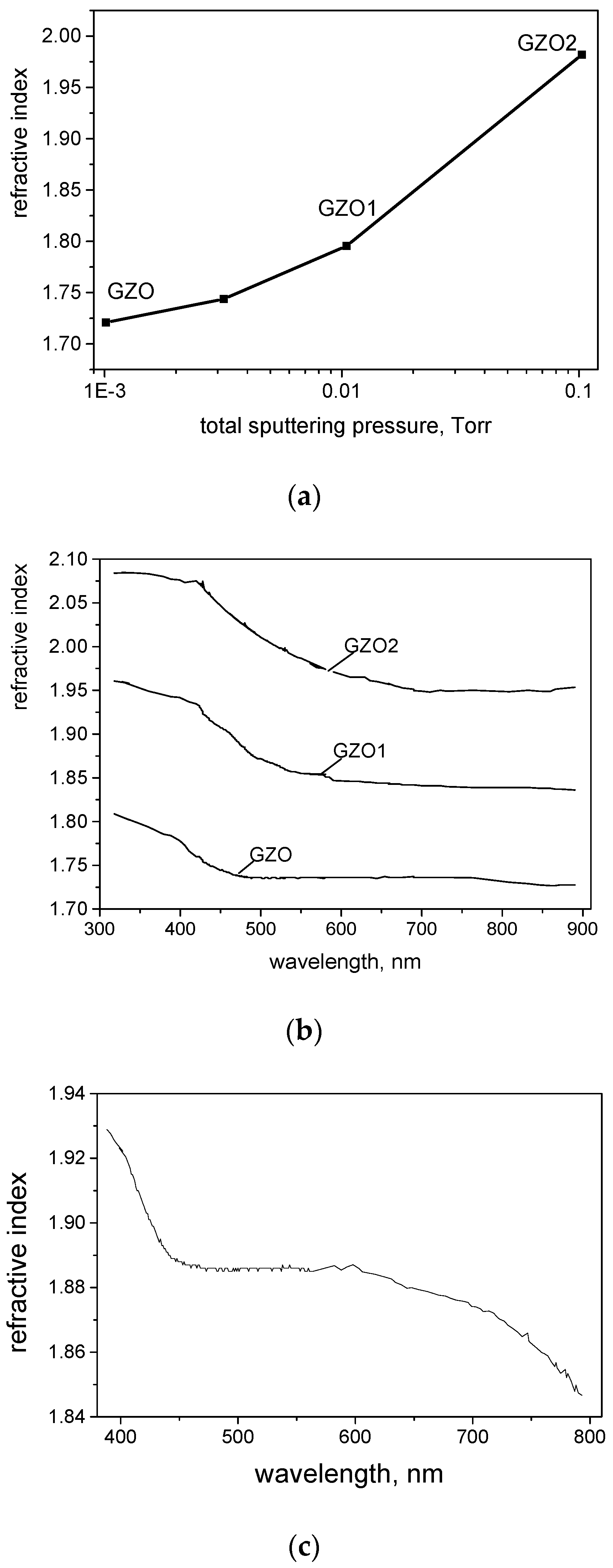
Figure 1. Refractive index of GZO sputtered at different total sputtering pressures due to additional target oxidation: (a) in the IR region; (b) in the whole spectrum range from UV to NIR. Sample GZO corresponds to non-additional oxidation, GZO1—to 10% additional oxidation, GZO2—to 20% additional oxidation; (c) refractive index of the ITO film [26].
Crystals 11 00137 g001
Figure 2. Electrical resistance of the bi-layer system ITO/GZO at different total sputtering pressures due to additional target oxidation [31].
Crystals 11 00137 g002
Figure 3. AFM images of (a) single GZO film; (b) bi-layer ITO/GZO without additional oxidation; (c) with 10% and (d) with 20% of additional oxidation.
Crystals 11 00137 g003
Figure 4. Optical transmittance in the UV-VIS range of single layer of GZO and bi-layer coatings ITO/GZO without and with additional oxidation during sputtering [31].
Crystals 11 00137 g004
Figure 5. Optical reflectionin the NIR range of single layer of GZO and bi-layercoatings ITO/GZO without and with additional oxidation during sputtering [31].
Crystals 11 00137 g005
Figure 6. Work function of the ITO/GZO films at various oxidation degrees: (a) UPS spectra for determination of the work function of ITO/GZO at different oxidation degree; (b) zoomed UPS spectrums (c) energy band diagram of CdS/ZnS core-shell quantum dots/perovskite solar cell with optimal ITO/GZO2 film as TCE.
Crystals 11 00137 g006aCrystals 11 00137 g006b
Publisher’s Note: MDPI stays neutral with regard to jurisdictional claims in published maps and institutional affiliations.