Abstract
The tunnel field-effect transistor (TFET) is a potential candidate for replacing the reverse diode and providing a secondary path in a whole-chip electrostatic discharge (ESD) protection network. In this paper, the ESD characteristics of a traditional point TFET, a line TFET and a Ge-source TFET are investigated using technology computer-aided design (TCAD) simulations, and an improved TFET-based whole-chip ESD protection scheme is proposed. It is found that the Ge-source TFET has a lower trigger voltage and higher failure current compared to the traditional point and line TFETs. However, the Ge-source TFET-based secondary path in the whole-chip ESD protection network is more vulnerable compared to the primary path due to the low thermal instability. Simulation results show that choosing the proper germanium mole fraction in the source region can balance the discharge ability and thermal failure risk, consequently enhancing the whole-chip ESD robustness.
1. Introduction
The phenomenon of band-to-band tunneling (BTBT) enables a tunnel field-effect transistor (TFET) to achieve smaller than a 60 mV/dec subthreshold swing (SS) at room temperature [1,2,3]. The integration of TFET and the conventional metal–oxide–semiconductor field-effect transistor (MOSFET) on the same silicon chip is a promising choice for future integrated circuits (ICs) [4]. Circuit implementations with both TFET and MOSFET proposed in the existing literature have achieved good performance [5,6,7,8]. Electrostatic discharge (ESD) protection is one of the key reliability issues of ICs, especially in advanced technologies [9,10]. Recently, silicon-based point TFETs have been investigated in the role of ESD protection devices and proposed for use in an ESD protection network [11,12,13,14]. It was verified that by using a TFET to replace the traditional diode in the whole-chip ESD protection network, the whole-chip ESD robustness can be improved since a secondary discharge path is added [14]. However, the results in the aforementioned literature show that the point TFET cannot make a significant contribution to the whole-chip ESD protection due to the low discharge capability. Therefore, it is necessary to search for a new TFET with different structures or different materials possessing higher discharge currents and lower trigger voltages compared to point TFETs.
In this paper, first, TFETs in different configurations are compared and it is found that the germanium-source (Ge-source) TFET has better ESD characteristics compared to the silicon point and line TFETs. Second, the application of the Ge-source TFET in the whole-chip ESD protection network is investigated, and the thermal instability of a Ge-source TFET induced failure is observed. Last, available solutions are discussed, and simulation results are analyzed in detail.
2. Model Calibration and Devices Structure
The simulations for this work were performed using the Sentaurus-TCAD tool. We used the non-local dynamic BTBT model, van Overstraeten–de Man avalanche generation model, high-field saturation model, Philips unified mobility model, thermodynamic model, band gap narrowing and Shockley–Read–Hall recombination models. The simulation parameters were calibrated by reproducing the experimental results of the TFET [14,15], which are presented in Figure 1a,b. It is evident that the experimental and simulated data agree with one another.
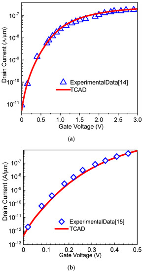
Figure 1.
Calibration of transfer curves of (a) point tunnel field-effect transistor (TFET), line TFET and (b) Ge-source TFET using experimental data.
The cross-sectional views of the point TFET, line TFET and Ge-source TFET used in this work are shown in Figure 2. The parameters are as follows: effective oxide thickness Tox = 1 nm, depth of the junction Xj = 30 nm, thickness of the pocket between the gate oxide and the source Tpocket = 3 nm, lengths of the drain and channel equal to 100 nm, length of gate–source overlap Lov = 80 nm, gate metal work function ϕ = 5 eV, p+ source doping NS = 1 × 1020 cm−3 (Ge-source TFET: NS = 1 × 1019 cm−3), n+ drain doping ND = 1 × 1020 cm−3 (Ge-source TFET: ND = 1 × 1019 cm−3) and p- substrate doping PSub = 1 × 1017 cm−3.
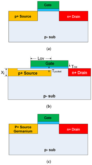
Figure 2.
Cross-sectional views of (a) silicon-based point TFET, (b) line TFET and (c) Ge-source TFET used in this work (not to scale).
3. Characteristics of the Three TFETs
3.1. Transfer Characteristics
As mentioned in [12,13], the TFETs subjected to an ESD stress have a BTBT-assisted avalanche generation mechanism. However, as the BTBT current of the point TFET is not high enough, the reduction in trigger voltage is still not satisfactory. Therefore, optimization of the TFET structure to increase the BTBT current can reduce the trigger voltage. Generally, the line TFET has a larger BTBT current than the point TFET because the tunneling area can be increased easily by enlarging the length of the gate–source overlap region (Lov) [16]. Using the germanium material in the source region can further increase the TFET’s current because the material has a narrower band gap and lower carrier effective mass than silicon and, consequently, the BTBT generation rate is increased [15,17]. Simulated transfer curves of the three types of TFETs are shown in Figure 3, where it can be observed that the Ge-source TFET has a significantly higher BTBT current under the same bias condition with a comparable device size.
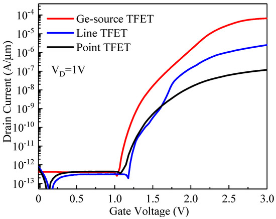
Figure 3.
Transfer curves of different TFETs.
The gates of TFETs can be connected to their own drains or sources. In this work, the gates are connected to the drains, and, in turn, the BTBT and avalanche generation both occur in proximity to the source/channel interface. Note that since a proper gate metal work function was used, the leakage currents under the normal operating condition (VG = VD = 1 V) are low enough, as shown in Figure 3.
3.2. Electrostatic Discharge Characteristics
Under the ESD event, the gate and drain voltages are both elevated when the current is injected into the drain terminals. The vertical electric field across the channel increases, the energy bands bend and, in turn, the BTBT current is generated. This current provides the initial carriers for avalanche generation, and, therefore, a relatively low breakdown voltage is obtained [13]. Figure 4 shows the contour plots of the BTBT generation and impact ionization rates of all three TFETs under the same applied voltage (3 V). It can be observed that the Ge-source TFET has a significantly higher BTBT generation rate and impact ionization rate.
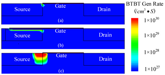
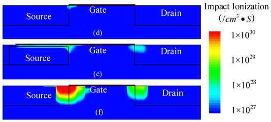
Figure 4.
Band-to-band tunneling generation rates of (a) point TFET, (b) line TFET and (c) Ge-source TFET, and impact ionization rates of (d) point TFET, (e) line TFET and (f) Ge-source TFET at a voltage pulse of 3 V.
Transmission line pulsing (TLP) simulation is widely used to estimate the behavior of ESD protection devices and circuits. In the simulation, the current pulse has a rise time of 10 ns and a pulse width of 100 ns to mimic the human body model ESD event [12,14]. The quasi-statistic characteristics are obtained by averaging the transient data in an interval of 60 to 90 ns. According to [18,19], the lattice temperature is usually used as the criterion to determine device failure in simulations. The critical failure temperature is usually defined as a value that is hundreds of degrees kelvin lower than the melting temperature. The critical failure temperatures of the full-silicon TFET and Ge-source TFET in the simulation are set to 1200 and 890 K, respectively.
Figure 5 shows the TLP curves of different TFETs and the reverse shallow-trench-isolation (STI) diode. The parameters of the reverse STI diode are consistent with TFETs. It is concluded that the quasi-static electrical characteristics of all TFETs are well compared to the reverse STI diode. The authors of [14] proved that point TEFTs can replace the reverse STI diode, and for this reason, this work will only discuss the comparison between TFETs. It is evident that under 0.1 mA/μm current pulse, the trigger voltage is as low as 2.3 V for Ge-source TFET, while it is 5.2 and 6.9 V for the line TFET and point TFET, respectively. As the voltage across the Ge-source TFET is significantly lower than that across the line TFET and point TFET, a lower amount of heat will be generated in the Ge-source TFET. Consequently, the failure current of the Ge-source TFET increases.
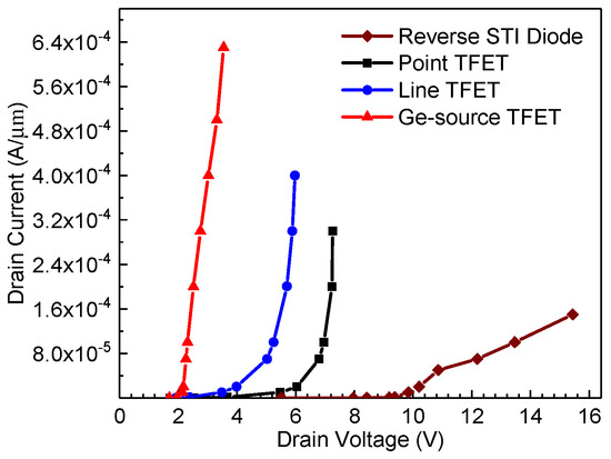
Figure 5.
Simulated transmission line pulsing (TLP) curves of different TFETs and the reverse shallow-trench-isolation (STI) diode.
The discharge capacity of the TFETs is higher than that of the traditional diodes seen in Figure 5. It should be noted that the above conclusion stands when the ESD current flows from the n+ region to the p+ region. When the ESD current flows from the p+ region to the n+ region, both the TFET and the diode operate in positive diode mode and thus have a similar discharge capability.
In order to evaluate the device characteristics under fast ESD events, such as the charged device model (CDM), a very fast TLP (VFTLP) current with a rise time and pulse width of 0.2 and 2 ns, respectively, is applied to the TFETs. The simulation curves are shown in Figure 6.
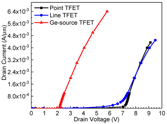
Figure 6.
Simulated very fast TLP (VFTLP) curves of different TFETs.
The results reveal that, as expected, the trigger voltage trend is the same as that obtained in the TLP simulation. However, the failure current of the line TFET is almost identical to that of the point TFET. This is because when the device is fully turned on, the BTBT current is no longer the dominant factor affecting the current conduction. The Ge-Source TFET still performs better than the other two TFETs. It should be mentioned that the failure current for the VFTLP simulation is higher than that for the TLP simulation because the VFTLP pulse width is significantly shorter than the TLP pulse width.
4. Whole-Chip ESD Protection Network with Different TFETs
Figure 7 shows the schematic of the whole-chip ESD protection network with TFETs, where the TFETs are connected to an input/output (I/O) pad instead of traditional diodes. The clamp circuit consists of a trigger circuit and a big MOSFET. The trigger circuit is implemented via a resistive-capacitive (RC) network with a 500 ns time constant, which ensures that the big MOSFET is in ON-state during the whole ESD event. The equivalent resistance of the metal wires is also considered.
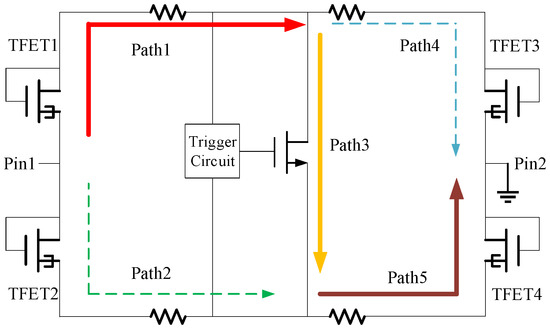
Figure 7.
Whole-chip electrostatic discharge (ESD) protection network.
In the whole-chip ESD protection, the pin-to-pin protection has the longest path and, therefore, the lowest robustness. The TFET is introduced to enhance the robustness, as shown in Figure 7. When the ESD current flows from pin1 to pin2, three discharge paths exist, i.e., the primary path path1-path3-path5 (Pp), the secondary path path2-path5 (Ps1) and path1-path4 (Ps2). Since TFET1 and TFET4 operate as positive biased p-n diodes, Pp has a relatively low conduction voltage and is the primary path. On the other hand, Ps1 and Ps2 with relatively high conduction voltages form the secondary paths. In the simulations, the TFETs and MOSFET have widths of 200 and 600 μm, respectively.
4.1. Basic TLP Simulation Results
A TLP current having an amplitude of 0.8 A is applied to the whole-chip protection networks with three different TFETs. Figure 8 shows the node voltage and path current at 20 ns. It can be observed that the clamping voltage is 5.01 V for the Ge-source TFET-based protection network, whereas the voltages are 6.64 and 6.68 V for the line and point TFET counterparts, respectively. This difference is due to a higher conduction of the current (0.23 A) by the Ge-source TFET compared to the line TFET (15.18 mA) and point TFET (1.38 mA). The point and line TFET-based protection networks pass the 0.8 A TLP test. The corresponding maximal temperatures are 1090 and 1066 K, respectively, which are lower than the default silicon failure temperature of 1200 K. On the contrary, the Ge-source TFET fails because the maximal temperature in the TFET reaches the default Ge failure temperature of 890 K at 55 ns, as shown in Figure 9. In fact, the failure current of the Ge-source TFET-based protection network is only 0.5 A.
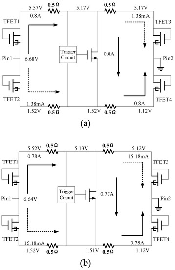
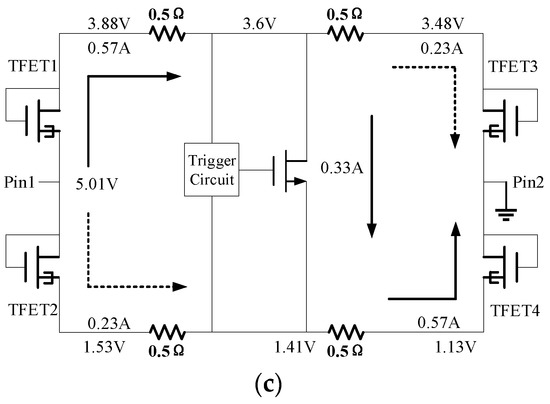
Figure 8.
Transmission line pulse response of (a) point TFET-, (b) line TFET- and (c) Ge-source TFET-based ESD networks.
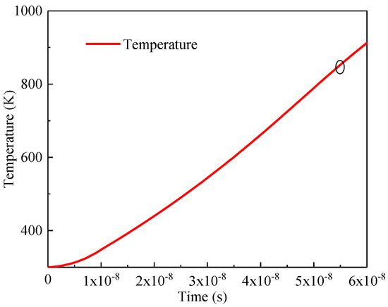
Figure 9.
Temperature versus time curve of the Ge-source TFET in the ESD protection network.
4.2. Thermal Instability of TFET-Based Protection Network
The early failure of the Ge-source TFET reduces the whole-chip ESD robustness, mainly because the Ge-source TFET has a low clamping voltage and excessive current flows through it. From Figure 8c, it can be noted that the Ge-source TFET discharges a current as high as 1.15 mA/μm, while its failure current is only 0.64 mA/μm, as shown in Figure 5. A large amount of current flows from the TFETs to the ground, generating excessive heat and causing failure. This behavior indicates that the TFET-based protection network has low thermal instability. As for the single device’s ESD robustness, the Ge-source TFET is better than the point and line TFETs. However, in the whole-chip ESD protection network, the current distribution significantly affects the failure location and determines the overall robustness. In the whole-chip protection network design, the TFETs should be properly designed to guarantee that the failure location appears in the MOSFET.
4.3. Optimization of the TFET-Based Protection Network
A ballast resistor is often introduced to improve the non-uniform conduction phenomenon in ESD protection [20]. However, this method is not suitable for the TFET-based whole-chip protection network because every TFET should have a ballast resistor, which significantly increases the serial resistance in the whole protection network and reduces the overall ESD robustness. An available solution is to reduce the Ge mole fraction in the source region, namely, using the silicon-germanium (SiGe) material rather than pure Ge in the source region. This reduction decreases the BTBT generation rate and impact ionization coefficient and, in turn, increases the breakdown voltage.
Figure 10 shows the node voltage and path current of the SiGe-source TFET-based ESD protection network under a 0.8 A current TLP simulation, in which the Ge mole fraction was set to 0.5. It can be noted that the clamping voltage increases from 5.01 to 6.11 V compared to the pure Ge-source TFET. However, this voltage is still lower than those in the point and line TFETs. As the SiGe-source TFETs conduct proper currents, the protection network does not fail even under a 1.1 A TLP simulation. The TFET and MOSFET maximal temperatures are 699 and 1150 K, respectively. Figure 11 shows the node voltage and path current under a 1.2 A TLP simulation. It can be observed that the Pin1 voltage starts to decrease and the current flowing through the MOSFET starts to increase at around 80 ns, indicating that thermal breakdown occurs in the MOSFET rather than the TFETs. A comparison of the four protection networks is shown in Table 1.
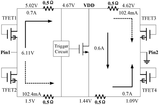
Figure 10.
Transmission line pulse response of the SiGe-source TFET-based ESD network.
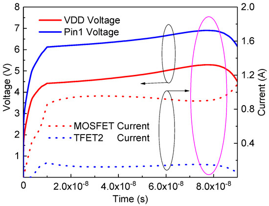
Figure 11.
Node voltage and device current under 1.2 A TLP simulation.

Table 1.
Comparison between four protection networks.
5. Conclusions
In this paper, the ESD characteristics of a point TFET, a line TFET and a Ge-source TFET were compared and their application in a whole-chip ESD protection network was evaluated using TCAD simulations. It was found that the Ge-source TFET had the best single-device ESD characteristics, especially a very low clamping voltage. However, in the whole-chip ESD protection, the Ge-source TFET-based network had the lowest robustness. This is because the Ge-source TFET had a very low clamping voltage and conducted excessive current, resulting in an early thermal failure. Simulation results show that a reduction in the Ge mole fraction in the source region limited the current flowing through the TFET, in turn increasing the whole-chip ESD robustness.
Author Contributions
Conceptualization, Z.Y. and Z.Z.; writing—original draft preparation, Z.Z.; writing—review and editing, Z.Z., Z.Y., X.F., Y.Z., J.J.L. and W.F. All authors have read and agreed to the published version of the manuscript.
Funding
This work was supported by the National Natural Science Foundation of China under Grant 61804123/61874098 and, in part, by the Key Research and Development Program of Shaanxi Province, China, under Grant 2019GY-018 and the Key Project Foundation of the Education Department of Shaanxi Province, China, under Grant 18JS082.
Institutional Review Board Statement
Not applicable.
Informed Consent Statement
Not applicable.
Data Availability Statement
Not applicable.
Conflicts of Interest
The authors declare no conflict of interest.
References
- Choi, W.Y.; Park, B.-G.; Lee, J.D.; Liu, T.-J.K. Tunneling field-effect transistors (TFETs) with subthreshold swing (SS) less than 60 mV/dec. IEEE Electron Device Lett. 2007, 28, 743–745. [Google Scholar] [CrossRef]
- Ionescu, A.M.; Riel, H. Tunnel field-effect transistors as energy efficient electronic switches. Nature 2011, 479, 329–337. [Google Scholar] [CrossRef] [PubMed]
- Lu, H.; Seabaugh, A. Tunnel field-effect transistors: State-of-the-art. IEEE J. Electron Devices Soc. 2014, 2, 44–49. [Google Scholar] [CrossRef]
- Han, K.; Wu, Y.; Huang, Y.C.; Xu, S.; Kumar, A.; Kong, E.; Kang, Y.; Zhang, J.; Wang, C.; Xu, H.; et al. First demonstration of complementary FinFETs and tunneling FinFETs co-integrated on a 200 mm GeSnOI substrate: A pathway towards future hybrid nano-electronics systems. In Proceedings of the 2019 Symposium on VLSI Technology, Kyoto, Japan, 9–14 June 2019. [Google Scholar]
- Chen, Y.-N.; Fan, M.-L.; Hu, P.-H.; Su, P.; Chuang, C.-T. Evaluation of stability, performance of ultra-low voltage MOSFET, TFET, and mixed TFET-MOSFET SRAM cell with write-assist circuits. IEEE J. Emerg. Sel. Top. Circuits Syst. 2014, 4, 389–399. [Google Scholar] [CrossRef]
- Lanuzza, M.; Strangio, S.; Crupi, F.; Palestri, P.; Esseni, D. Mixed tunnel-FET/MOSFET level shifters: A new proposal to extend the tunnel-FET application domain. IEEE Trans. Electron Devices 2015, 62, 3973–3979. [Google Scholar] [CrossRef]
- Hung, J.-H.; Wang, P.-Y.; Lo, Y.-C.; Yang, C.-W.; Tsui, B.-Y.; Yang, C.-H. Digital Logic and Asynchronous Datapath with Heterogeneous TFET-MOSFET Structure for Ultralow-Energy Electronics. IEEE J. Explor. Solid-State Comput. Devices Circuits 2020. [Google Scholar] [CrossRef]
- Wang, Z.; Zhong, Y.; Chen, C.; Ye, L.; Huang, Q.; Yang, L.; Huang, R. Ultra-low power hybrid TFET-MOSFET topologies for standard logic cells with improved comprehensive performance. In Proceedings of the 2019 IEEE International Symposium on Circuits and Systems (ISCAS), Sapporo, Japan, 26–29 May 2019; pp. 1–5. [Google Scholar]
- Mergens, M.P.J.; Russ, C.C.; Verhaege, K.G.; Armer, J.; Jozwiak, P.C.; Mohn, R.P.; Keppens, B.; Trinh, C.S. Speed optimized diode triggered SCR (DTSCR) for RF ESD protection of ultra-sensitive IC nodes in advanced technologies. IEEE Trans. Device Mater. Rel. 2005, 5, 532–542. [Google Scholar] [CrossRef]
- Galy, P. ElectroStatic Discharge (ESD) one real life event: Physical impact and protection challenges in advanced CMOS technologies. In Proceedings of the 2014 International Semiconductor Conference (CAS), Sinaia, Romania, 13–15 October 2014. [Google Scholar]
- Galy, P.; Athanasiou, S. Preliminary results on TFET-gated diode in thin silicon film for IO design & ESD protection in 28nm UTBB FD-SOI CMOS technology. In Proceedings of the 2016 International Conference on IC Design and Technology (ICICDT), Ho Chi Minh City, Vietnam, 27–29 June 2016. [Google Scholar]
- Kranthi, N.K.; Shrivastava, M. ESD behavior of tunnel FET devices. IEEE Trans. Electron Devices 2017, 64, 28–36. [Google Scholar] [CrossRef]
- Yang, Z.; Zhang, Y.; Yang, Y.; Yu, N. Investigation of the double current path phenomenon in gate grounded tunnel FET. IEEE Electron Device Lett. 2018, 39, 103–106. [Google Scholar] [CrossRef]
- Sithanandam, R.; Kumar, M.J. A new on-chip ESD strategy using TFETs-TCAD based device and network simulations. IEEE J. Electron Devices Soc. 2018, 6, 298–308. [Google Scholar] [CrossRef]
- Kim, S.H.; Agarwal, S.; Jacobson, Z.A.; Matheu, P.; Hu, C.; Liu, T.K. Tunnel Field Effect Transistor with Raised Germanium Source. IEEE Electron Device Lett. 2010, 31, 1107–1109. [Google Scholar] [CrossRef]
- Verreck, D.; Verhulst, A.S.; Kao, K.; Vandenberghe, W.G.; de Meyer, K.; Groeseneken, G. Quantum Mechanical Performance Predictions of p-n-i-n Versus Pocketed Line Tunnel Field-Effect Transistors. IEEE Trans. Electron Devices 2013, 60, 2128–2134. [Google Scholar] [CrossRef]
- Kim, S.H.; Kam, H.; Hu, C.; Liu, T.-J.K. Ge-source tunnel field effect transistors with record high ION/IOFF. In Proceedings of the 2009 Symposium on VLSI Technology, Honolulu, HI, USA, 15–17 June 2009. [Google Scholar]
- Wang Albert, Z.H. On-Chip ESD Protection for Integrated Circuits: An IC Design Perspective; Springer: New York, NY, USA, 2002; p. 233. [Google Scholar]
- Yang, Z.; Yang, Y.; Yu, N.; Liou, J.J. Improving ESD Protection Robustness Using SiGe Source/Drain Regions in Tunnel FET. Micromachines 2018, 9, 657. [Google Scholar] [CrossRef] [PubMed]
- Boschke, R.; Chen, S.H.; Scholz, M.; Hellings, G.; Linten, D.; Witters, L.; Groeseneken, G. ESD ballasting of Ge FinFET ggNMOS devices. In Proceedings of the IEEE International Reliability Physics Symposium, Monterey, CA, USA, 2–6 April 2017. [Google Scholar]
Publisher’s Note: MDPI stays neutral with regard to jurisdictional claims in published maps and institutional affiliations. |
© 2021 by the authors. Licensee MDPI, Basel, Switzerland. This article is an open access article distributed under the terms and conditions of the Creative Commons Attribution (CC BY) license (http://creativecommons.org/licenses/by/4.0/).