
Comprehensive Study and Optimization of Implementing p-NiO in β-Ga2O3 Based Diodes via TCAD Simulation


Abstract
:1. Introduction
2. Simulation Methodology
3. Results and Discussion
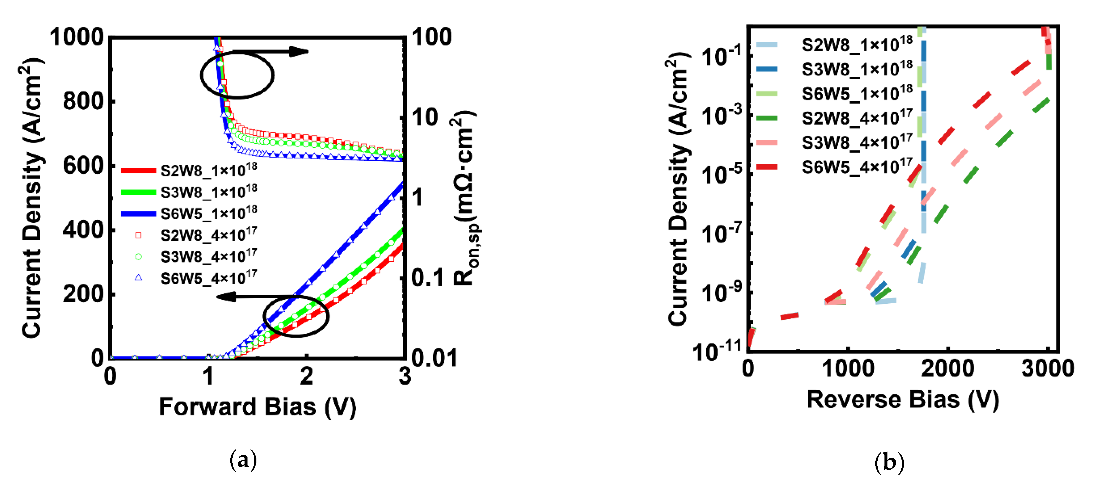
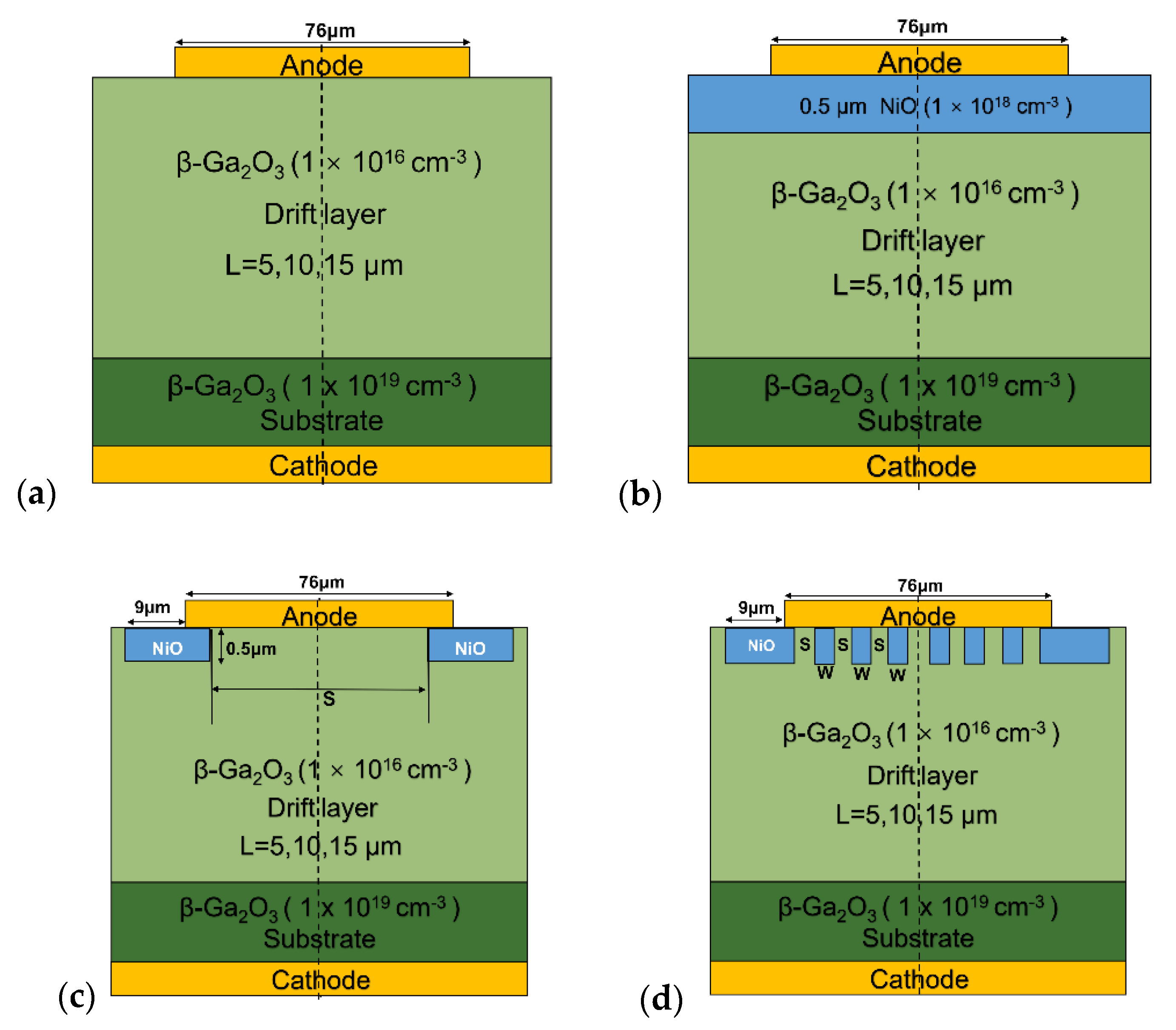
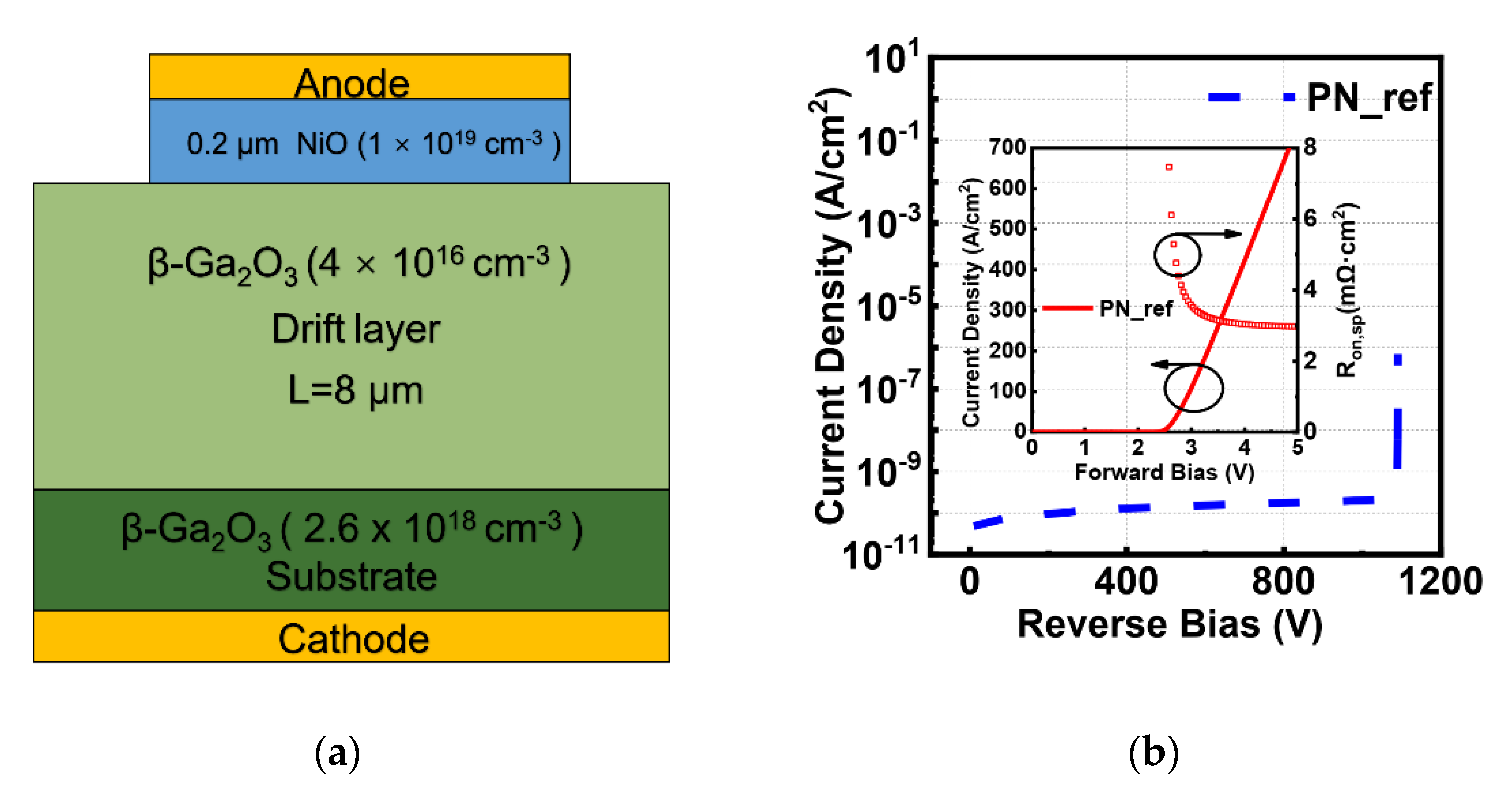
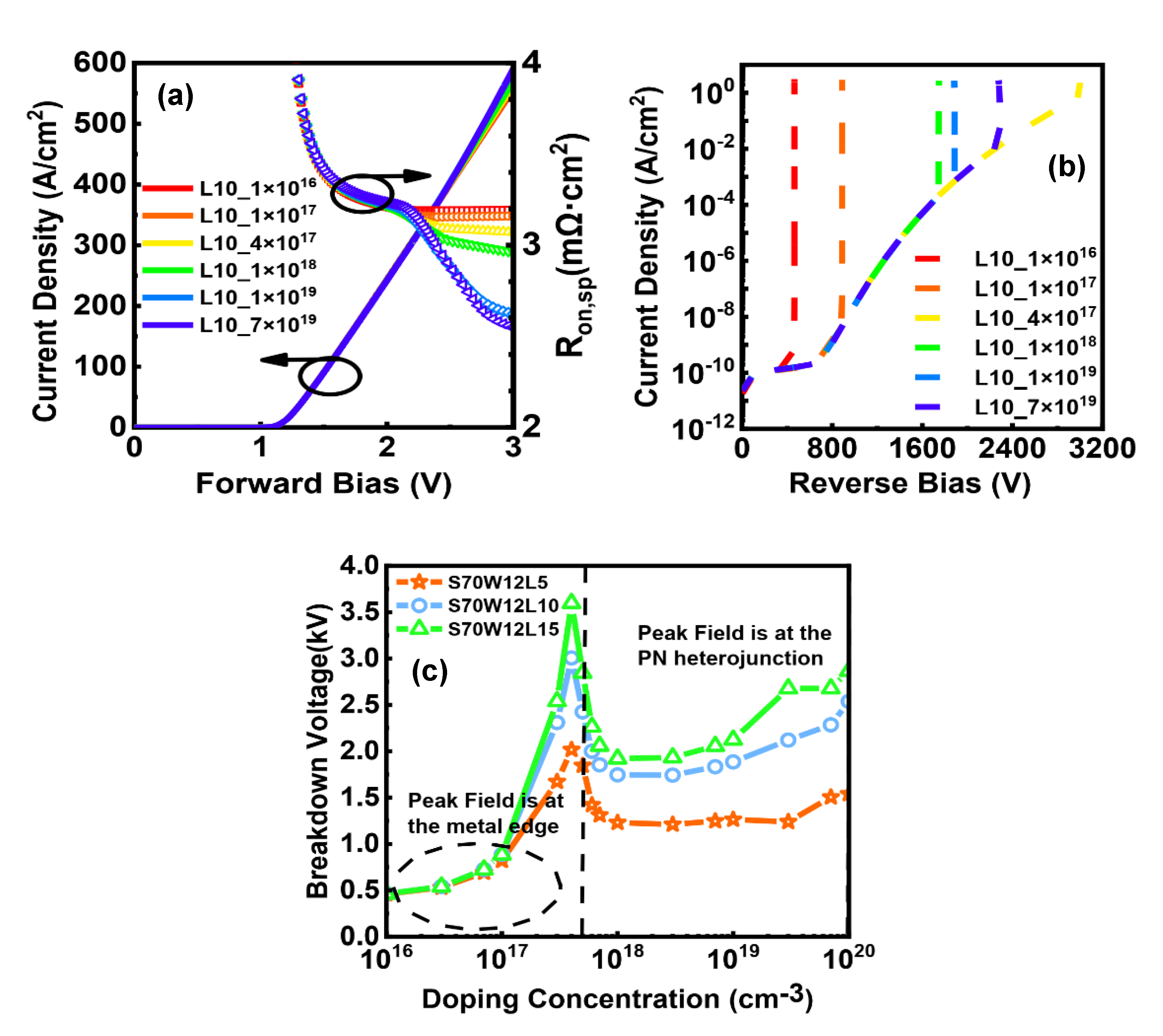
3.1. HJ PN Diode
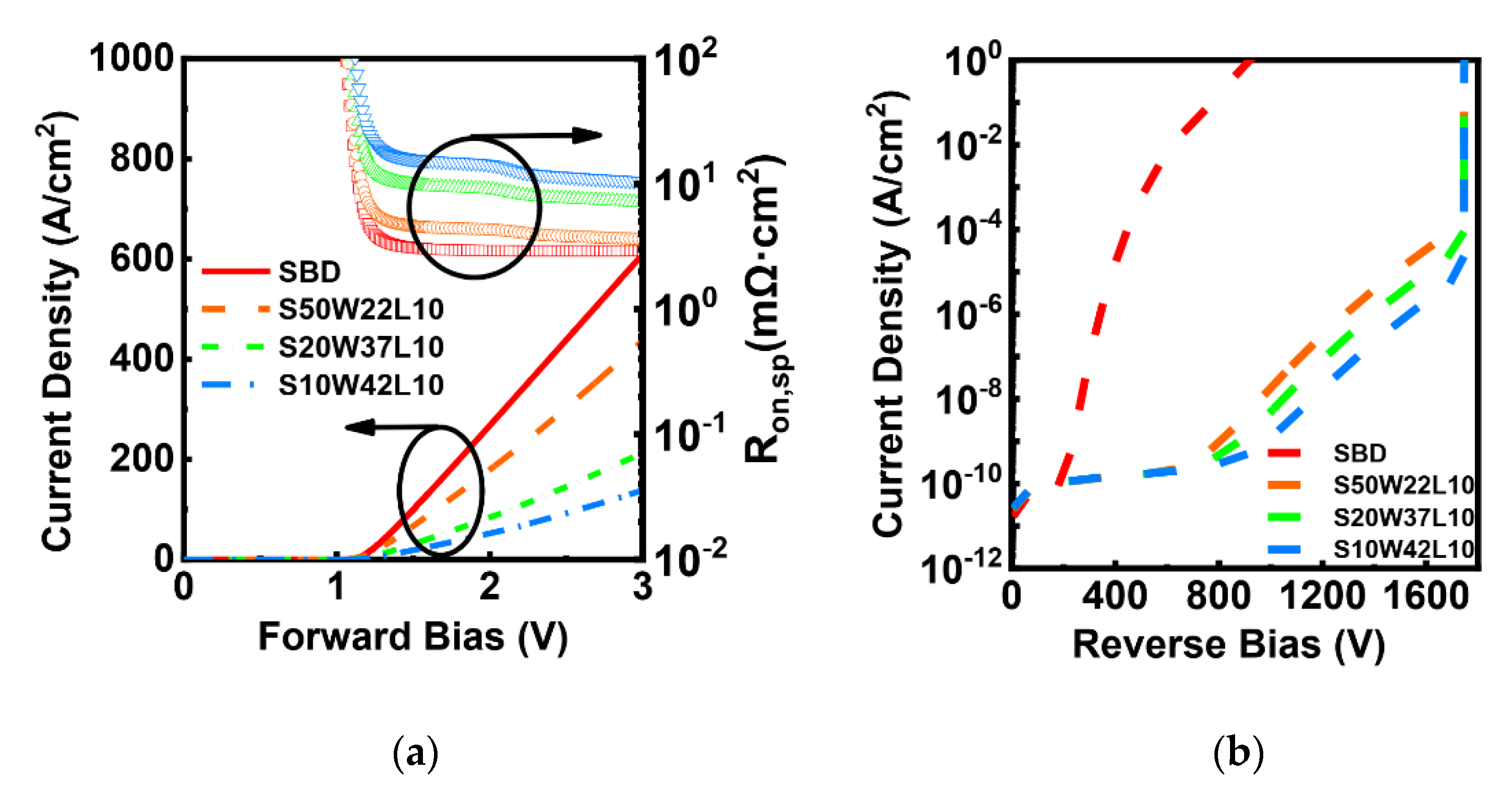
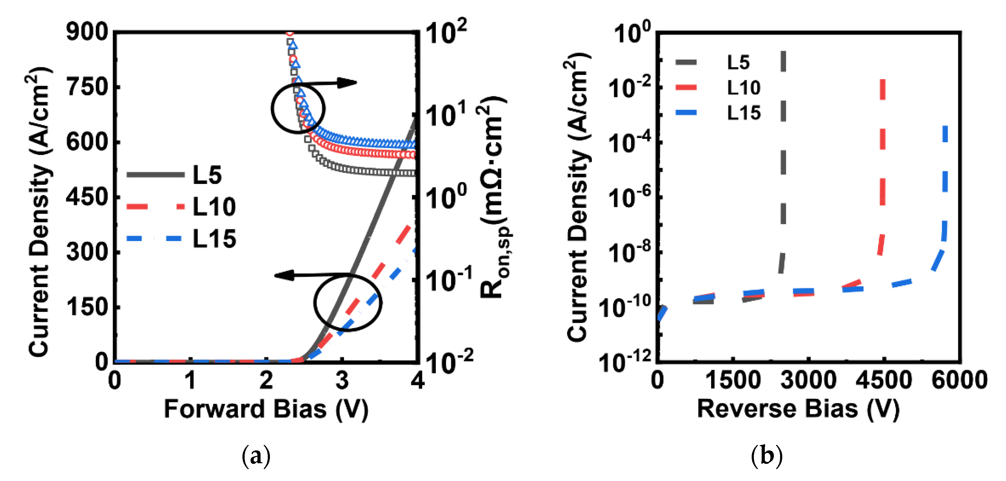
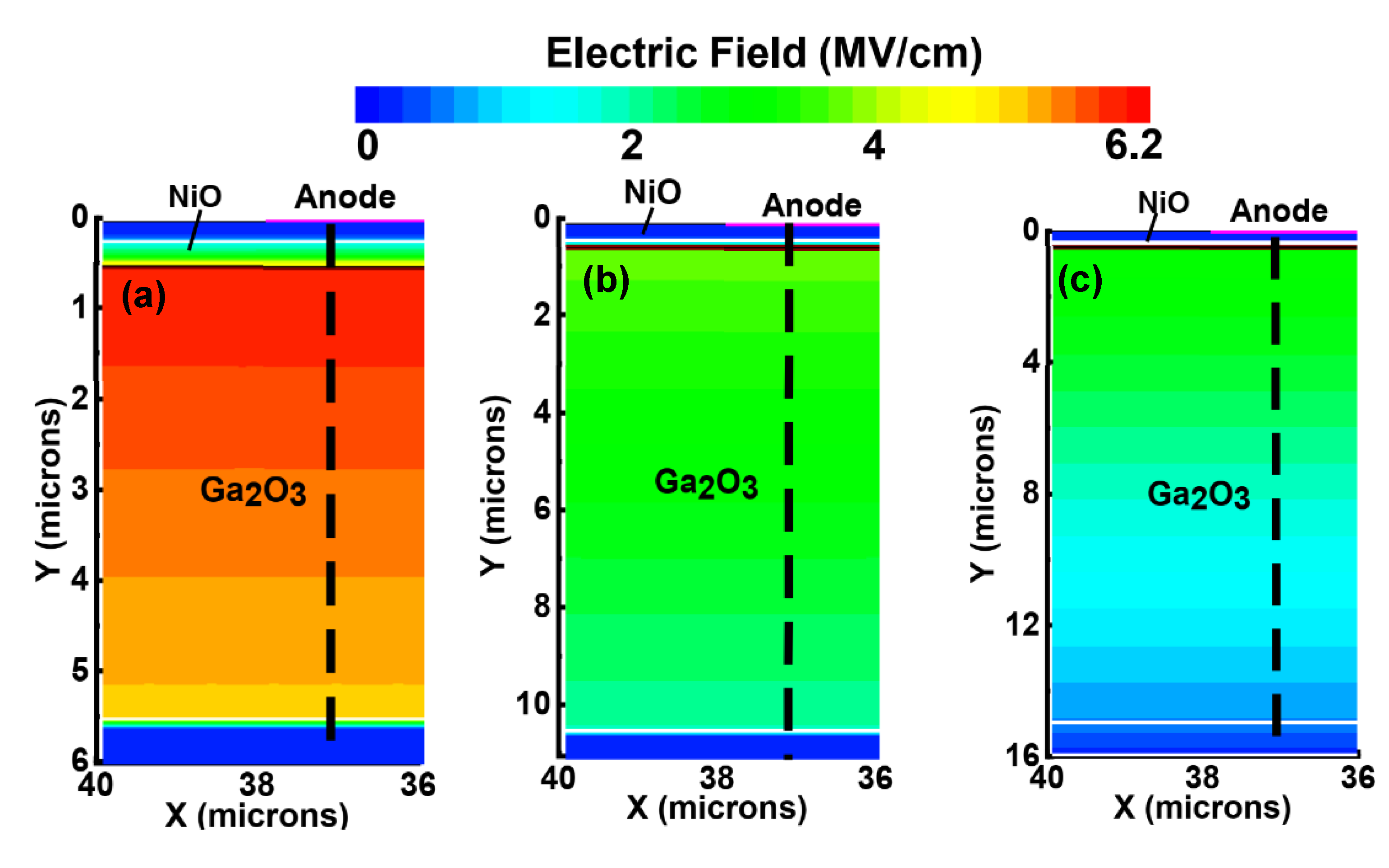
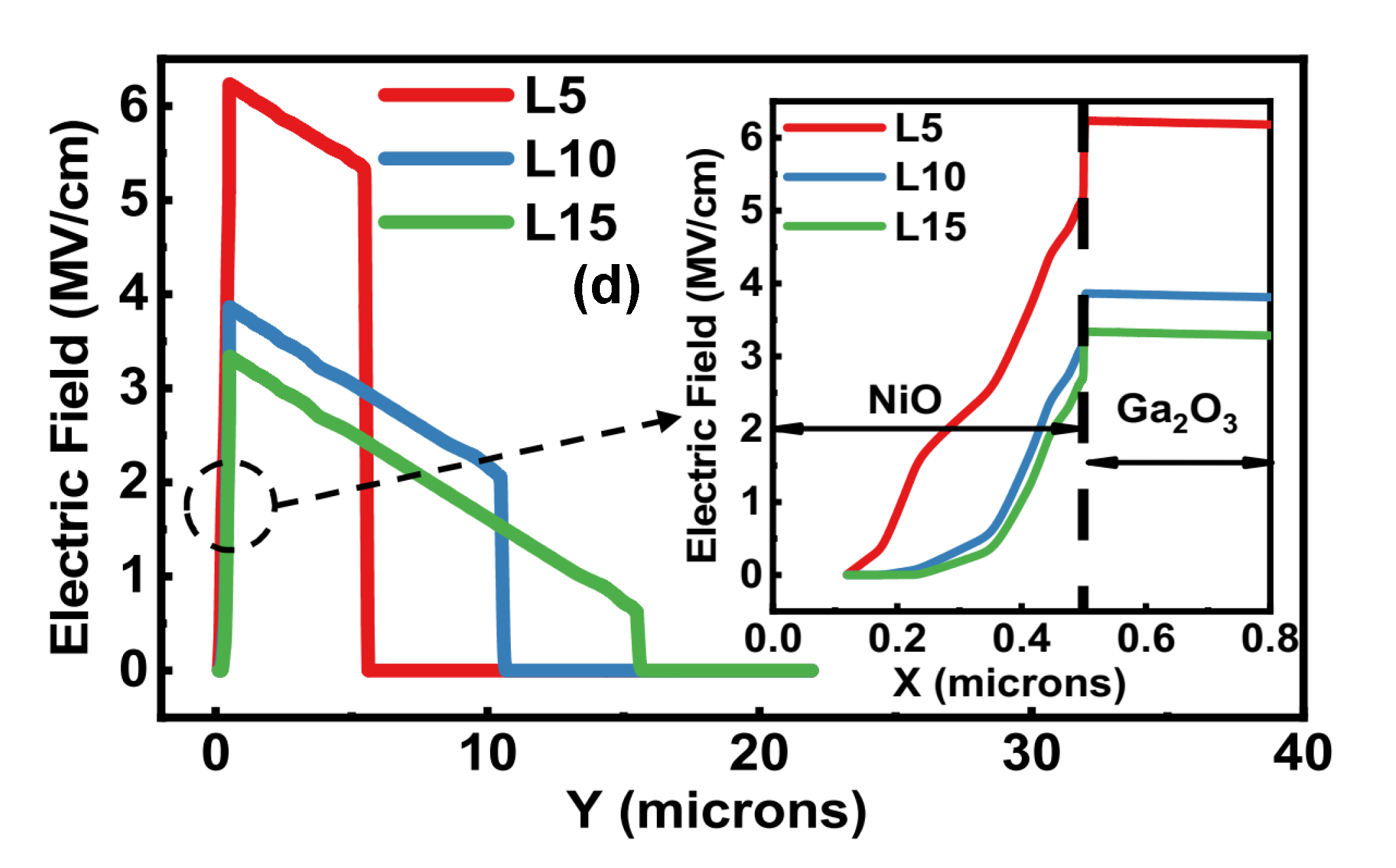
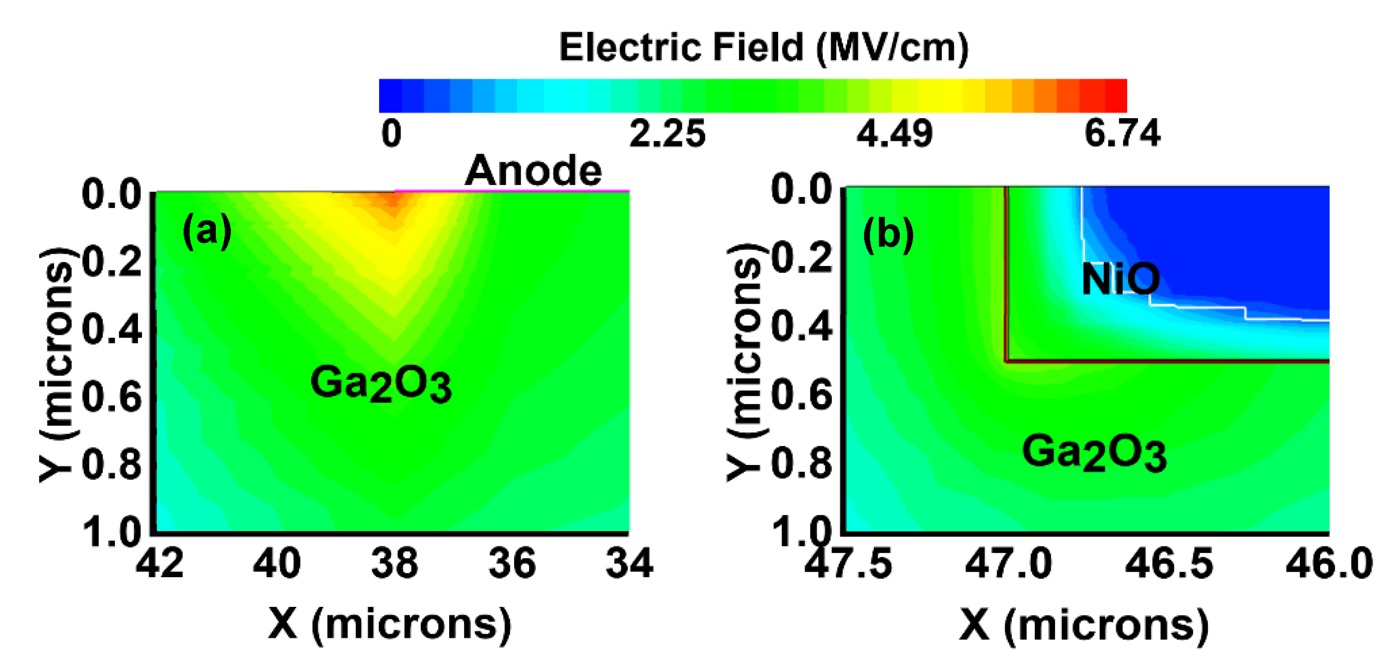
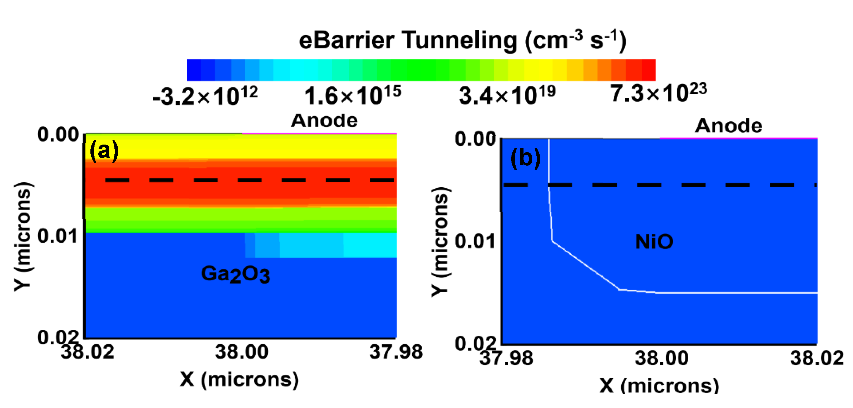
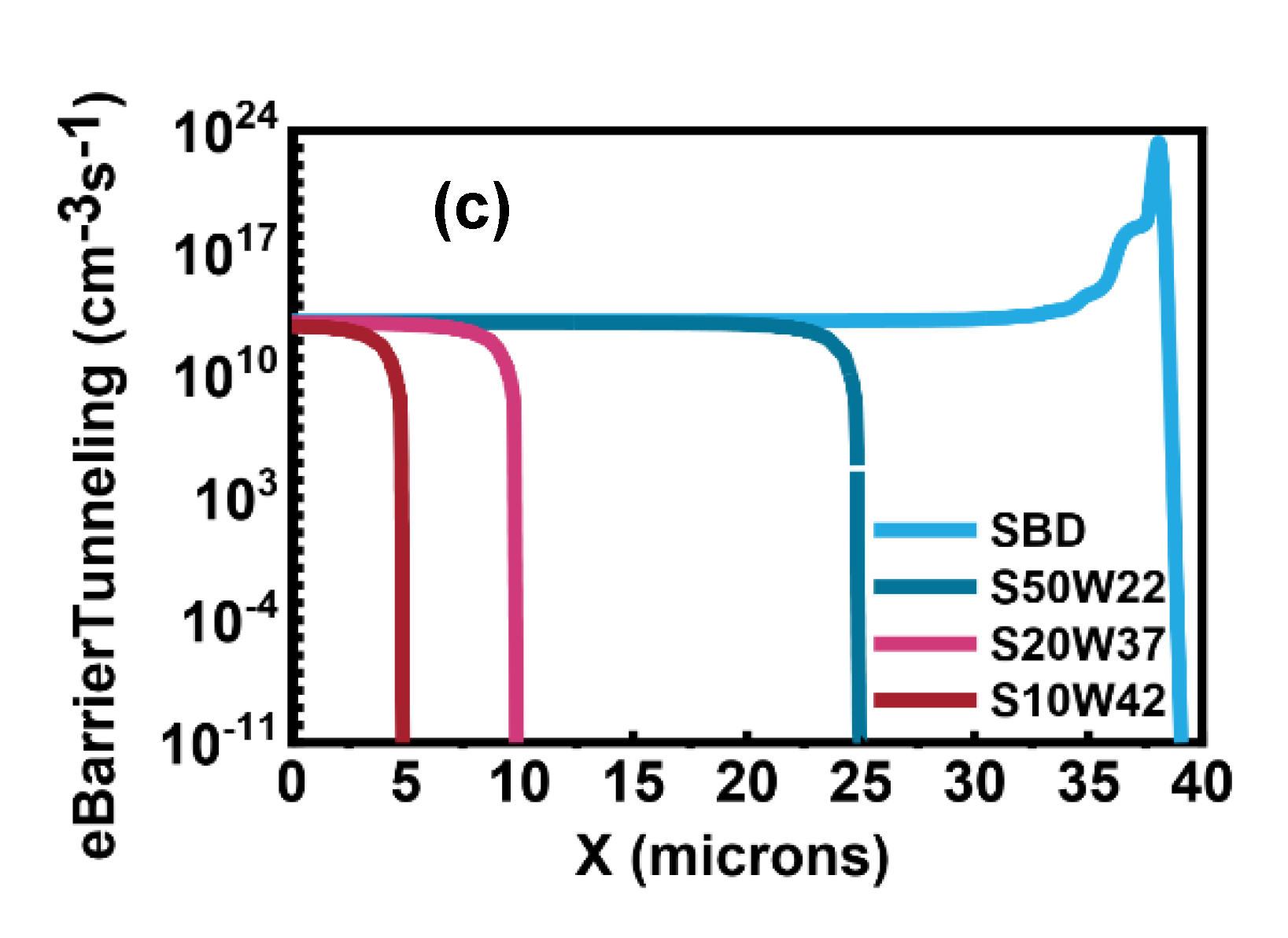
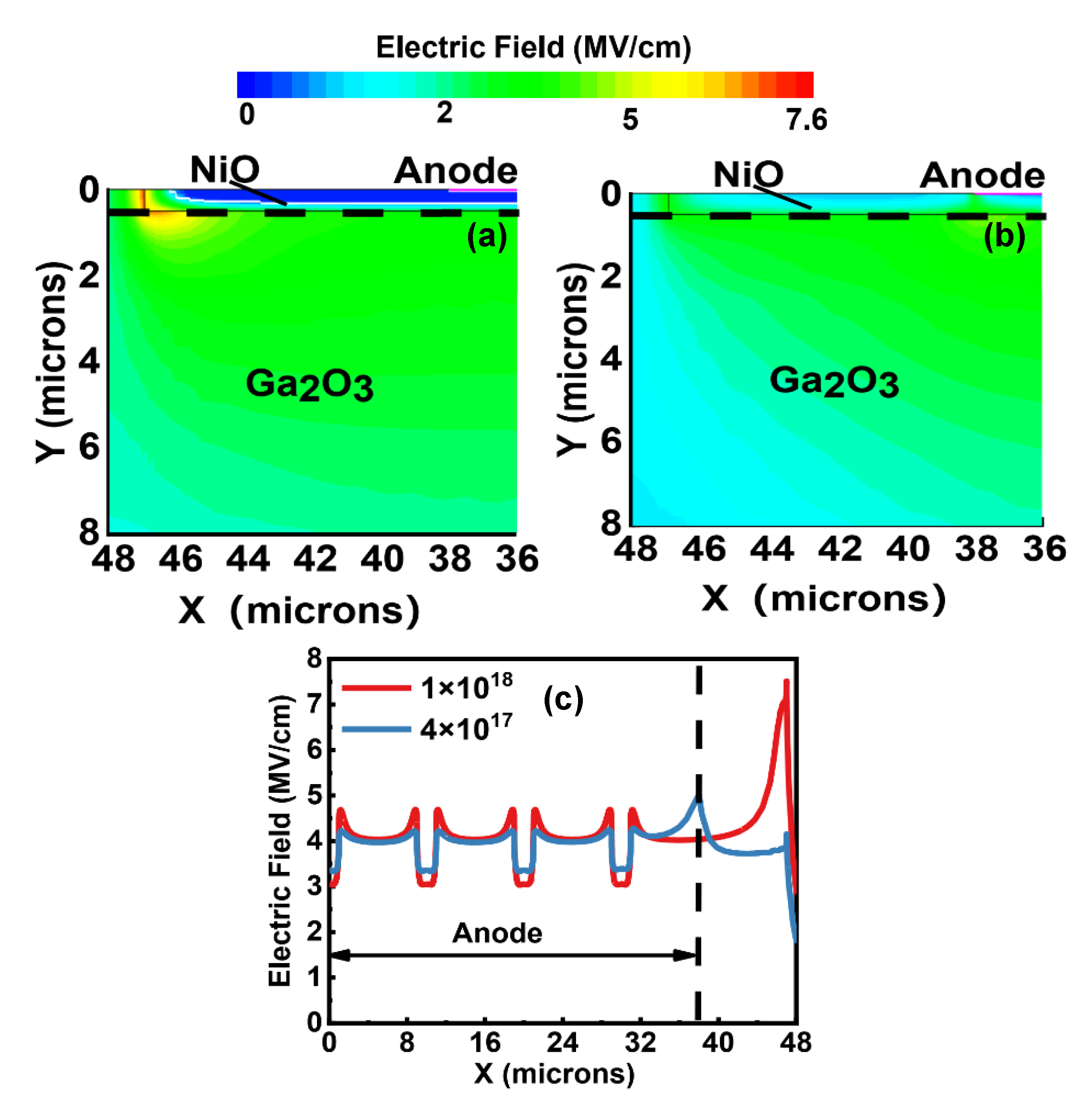
3.2. SBD with GRs
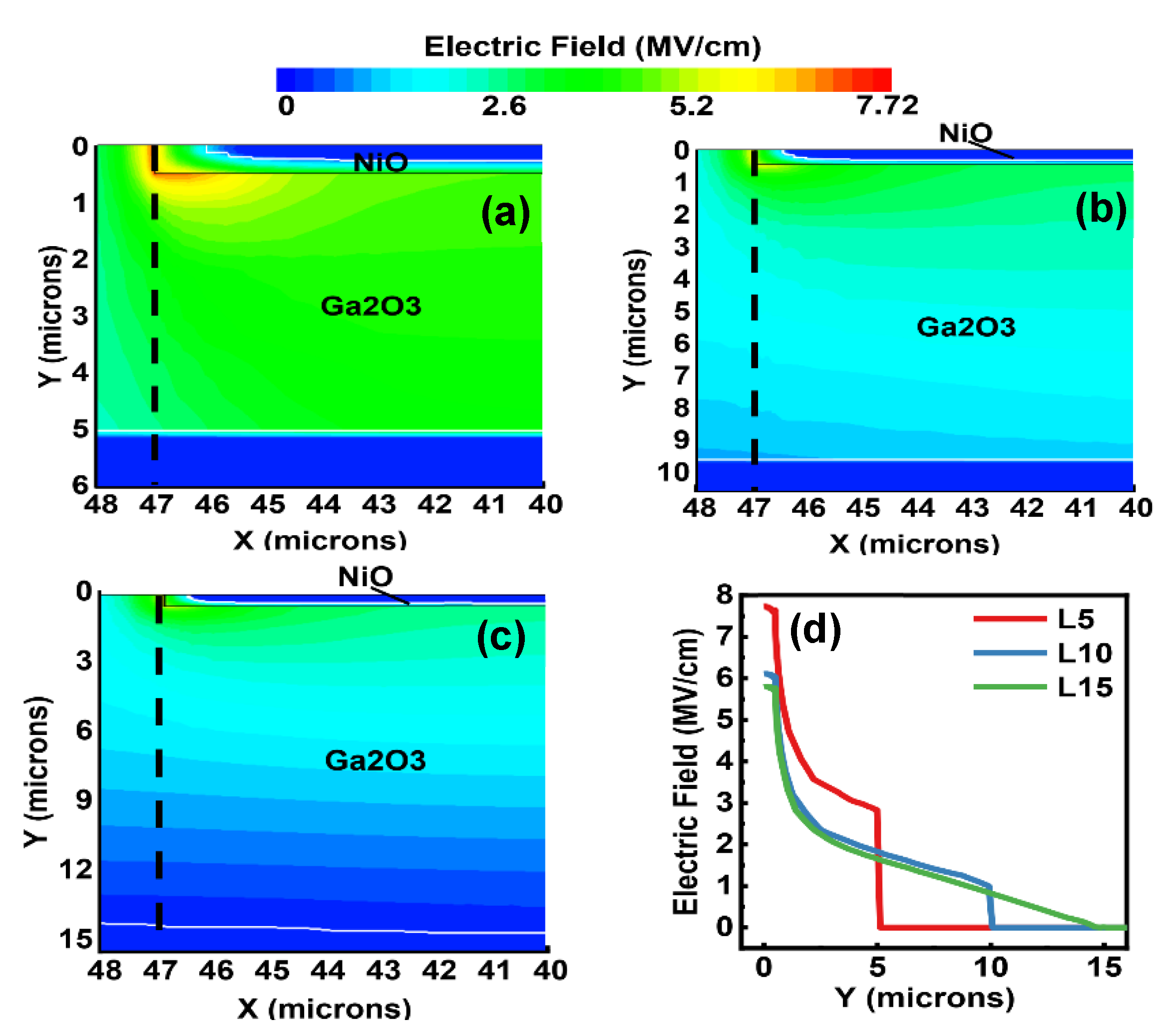
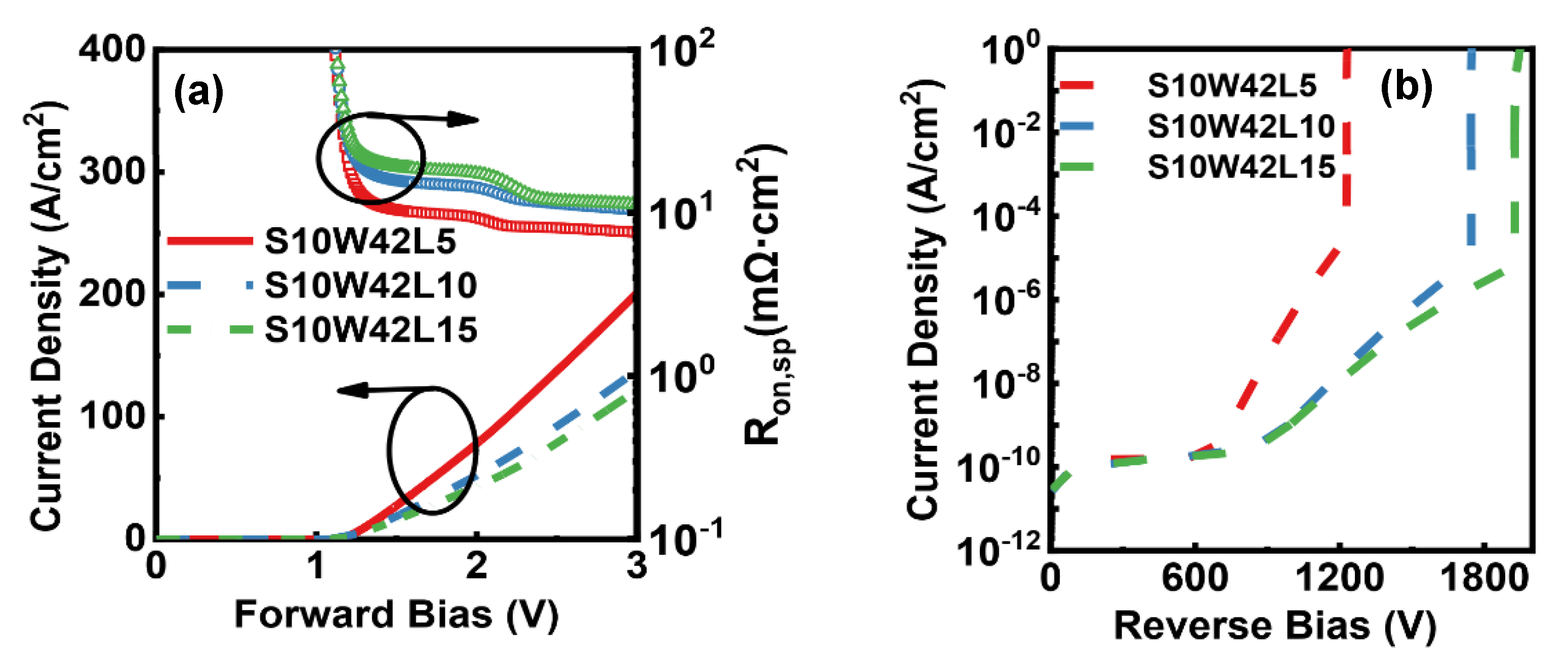
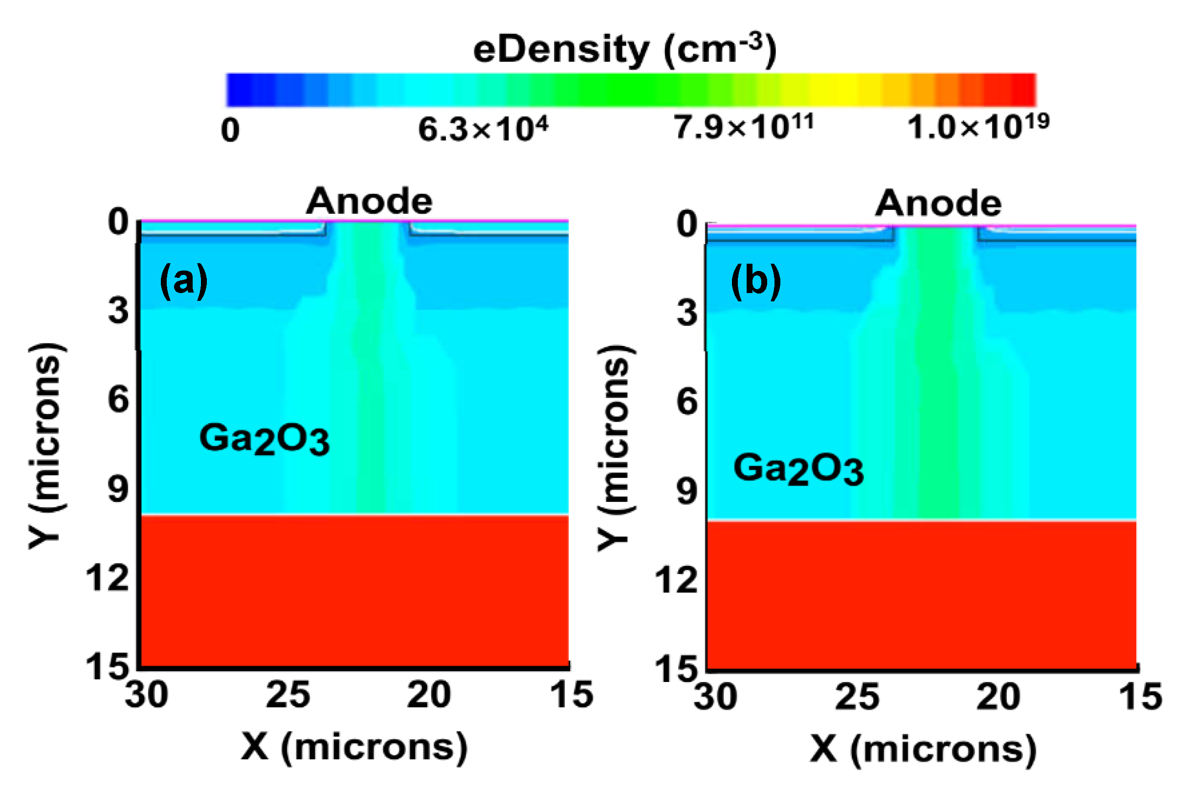
3.3. HJBS Diode
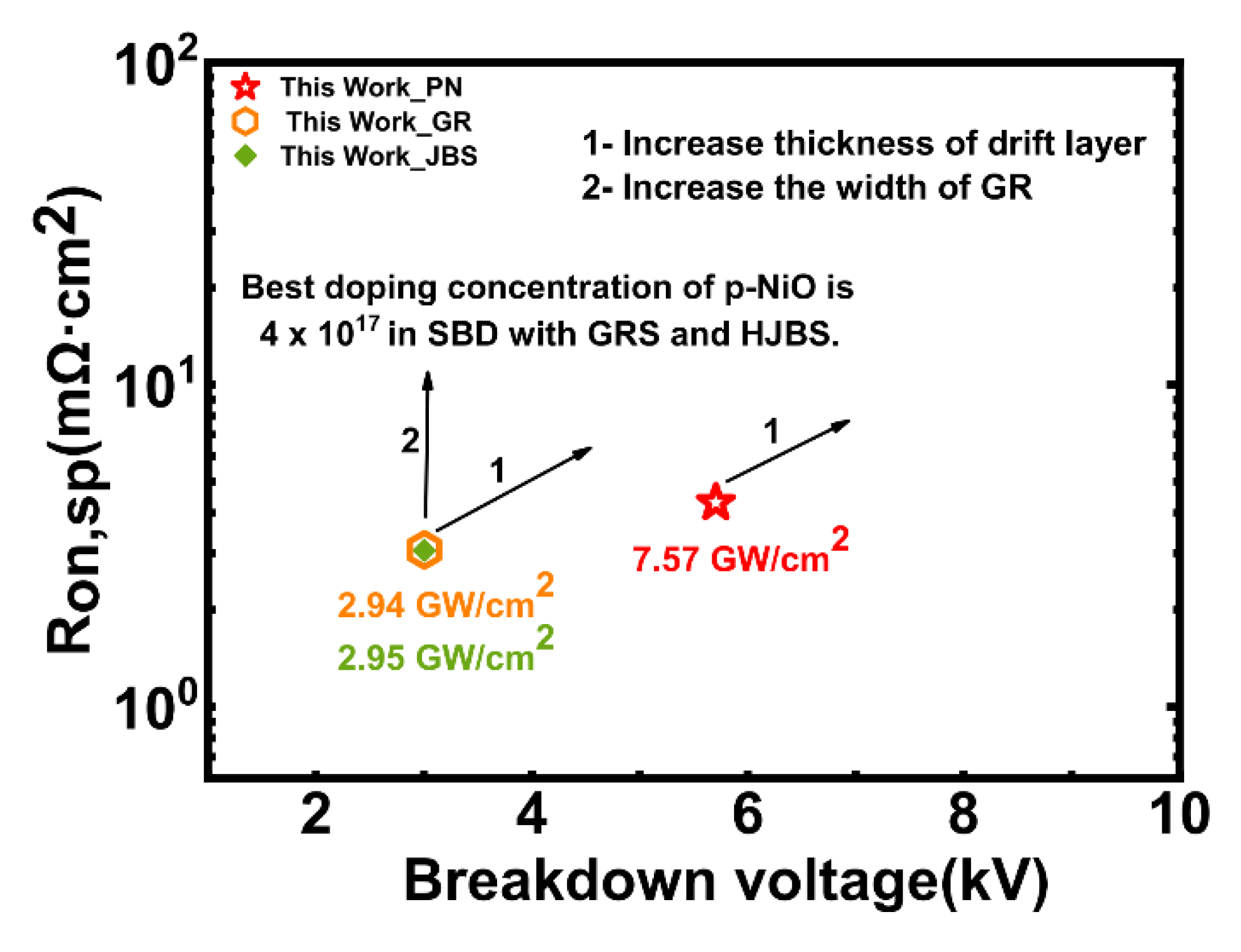
4. Conclusions
Author Contributions
Funding
Conflicts of Interest
References
- Pearton, S.J.; Yang, J.; Cary, P.H.; Ren, F.; Mastro, M.A. A review of Ga2O3 materials, processing, and devices. Appl. Phys. Rev. 2018, 5, 011301. [Google Scholar] [CrossRef] [Green Version]
- Higashiwaki, M.; Jessen, G.H. Guest Editorial: The dawn of gallium oxide microelectronics. Appl. Phys. Lett. 2018, 112, 060401. [Google Scholar] [CrossRef] [Green Version]
- Kuramata, A.; Koshi, K.; Watanabe, S.; Yamaoka, Y.; Masui, T.; Yamakoshi, S. High-quality β-Ga2O3 single crystals grown by edge-defined film-fed growth. Jpn. J. Appl. Phys. 2016, 55, 1202A2. [Google Scholar] [CrossRef]
- Galazka, Z.; Irmscher, K.; Uecker, R.; Bertram, R.; Pietsch, M.; Kwasniewski, A.; Naumann, M.; Schulz, T.; Schewski, R.; Klimm, D. On the bulk β-Ga2O3 single crystals grown by the Czochralski method. J. Cryst. Growth 2014, 404, 184–191. [Google Scholar] [CrossRef]
- Irmscher, K.; Galazka, Z.; Pietsch, M.; Uecker, R.; Fornari, R. Electrical properties of β-Ga2O3 single crystals grown by the Czochralski method. J. Appl. Phys. 2011, 110, A316–A350. [Google Scholar] [CrossRef]
- Baliga, B.J. Power semiconductor device figure of merit for high-frequency applications. IEEE Electron. Device Lett. 1989, 10, 455–457. [Google Scholar] [CrossRef]
- Konishi, K.; Goto, K.; Murakami, H.; Kumagai, Y.; Kuramata, A.; Yamakoshi, S.; Higashiwaki, M. 1-kV vertical Ga2O3 field-plated Schottky barrier diodes. Appl. Phys. Lett. 2017, 110, 103506. [Google Scholar] [CrossRef]
- Kumar, N.; Joishi, C.; Xia, Z.; Rajan, S.; Kumar, S. Electrothermal Characteristics of Delta-Doped beta-Ga2O3 Metal-Semiconductor Field-Effect Transistors. IEEE Trans. Electron. Devices 2019, 66, 5360–5366. [Google Scholar] [CrossRef]
- Sharma, S.; Zeng, K.; Saha, S.; Singisetti, U. Field-Plated Lateral Ga2O3 MOSFETs with Polymer Passivation and 8.03 kV Breakdown Voltage. IEEE Electron. Device Lett. 2020, 41, 836–839. [Google Scholar] [CrossRef]
- Li, W.; Nomoto, K.; Hu, Z.; Nakamura, T.; Xing, H.G. Single and multi-fin normally-off Ga2O3 vertical transistors with a breakdown voltage over 2.6 kV. In Proceedings of the 2019 IEEE International Electron Devices Meeting (IEDM), San Francisco, CA, USA, 7–11 December 2019. [Google Scholar]
- Hu, Z.; Hong, Z.; Qian, F.; Zhang, J.; Zhang, C.; Dang, K.; Cai, Y.; Feng, Z.; Gao, Y.; Kang, X. Field-Plated Lateral β-Ga2O3 Schottky Barrier Diode with High Reverse Blocking Voltage of More Than 3 kV and High DC Power Figure-of-Merit of 500 MW/cm2. IEEE Electron. Device Lett. 2018, 39, 1564–1567. [Google Scholar] [CrossRef]
- Zhou, H.; Yan, Q.L.; Zhang, J.C.; Lv, Y.J.; Liu, Z.H. High-Performance Vertical β-Ga2O3 Schottky Barrier Diode With Implanted Edge Termination. IEEE Electron. Device Lett. 2019, 40, 1788–1791. [Google Scholar] [CrossRef]
- Li, W.; Nomoto, K.; Hu, Z.; Jena, D.; Xing, H.G. Field-Plated Ga2O3 Trench Schottky Barrier Diodes with a BV2/Ron,sp of up to 0.95 GW/cm2. IEEE Electron. Device Lett. 2019, 41, 107–110. [Google Scholar] [CrossRef]
- Zhou, H.; Zhang, J.; Zhang, C.; Feng, Q.; Hao, Y. A review of the most recent progresses of state-of-art gallium oxide power devices. J. Semicond. 2019, 40, 011803. [Google Scholar] [CrossRef]
- Varley, J.B.; Janotti, A.; Franchini, C.; Van de Walle, C.G. Role of self-trapping in luminescence and p-type conductivity of wide-band-gap oxides. Phys. Rev. B Condens. Matter Mater. Phys. 2012, 85, 081109. [Google Scholar] [CrossRef] [Green Version]
- Lu, X.; Zhou, X.; Jiang, H.; Ng, K.r.W.; Wang, G. 1-kV sputtered p-NiO/n-Ga2O3 heterojunction diodes with an ultra-low leakage current below 1 μA/cm2. IEEE Electron. Device Lett. 2020, 41, 449–452. [Google Scholar] [CrossRef]
- Gong, H.H.; Chen, X.H.; Xu, Y.; Ren, F.F.; Ye, J.D. A 1.86-kV double-layered NiO/β-Ga2O3 vertical p-n heterojunction diode. Appl. Phys. Lett. 2020, 117, 22104. [Google Scholar] [CrossRef]
- Kokubun, Y.; Kubo, S.; Nakagomi, S. All-oxide p–n heterojunction diodes comprising p-type NiO and n-type β-Ga2O3. Appl. Phys. Express 2016, 9, 091101. [Google Scholar] [CrossRef]
- Watahiki, T.; Yu Da, Y.; Furukawa, A.; Yamamuka, M.; Takiguchi, Y.; Miyajima, S. Heterojunction p-Cu2O/n-Ga2O3 diode with high breakdown voltage. Appl. Phys. Lett. 2017, 111, 222104. [Google Scholar] [CrossRef]
- Vera, F.; Schrebler, R.; Munoz, E.; Suarez, C.; Cury, P.; Gomez, H.; Cordova, R.; Marotti, R.; Dalchiele, E. Preparation and characterization of Eosin B- and Erythrosin J-sensitized nanostructured NiO thin film photocathodes. Thin Solid Film. 2005, 490, 182–188. [Google Scholar] [CrossRef]
- Lu, Y.M.; Hwang, W.S.; Yang, J.S. Effects of substrate temperature on the resistivity of non-stoichiometric sputtered NiOx films. Surf. Coat. Technol. 2002, 155, 231–235. [Google Scholar] [CrossRef]
- Tyagi, M.; Tomar, M.; Gupta, V. P-N Junction of NiO Thin Film for Photonic Devices. IEEE Electron. Device Lett. 2013, 34, 81–83. [Google Scholar] [CrossRef]
- Yan, Q.; Gong, H.; Zhang, J.; Ye, J.; Hao, Y. β-Ga2O3 hetero-junction barrier Schottky diode with reverse leakage current modulation and BV2 /Ron,sp value of 0.93 GW/cm2. Appl. Phys. Lett. 2021, 118, 122102. [Google Scholar] [CrossRef]
- Nan, M.; Tanen, N.; Verma, A.; Zhi, G.; Luo, T.; Xing, H.; Jena, D. Intrinsic Electron Mobility Limits in beta-Ga2O3. Appl. Phys. Lett. 2016, 109, 212101. [Google Scholar]
- Gielisse, P.J.; Plendl, J.N.; Mansur, L.C.; Marshall, R.; Smakula, A. Infrared Properties of NiO and CoO and Their Mixed Crystals. J. Appl. Phys. 1965, 36, 2446–2450. [Google Scholar] [CrossRef]
- Hudgins, J.L.; Simin, G.S.; Santi, E.; Khan, M.A. An assessment of wide bandgap semiconductors for power devices. IEEE Trans. Power Electron. 2003, 18, 907–914. [Google Scholar] [CrossRef] [Green Version]


| Material | Ga2O3 | NiO |
|---|---|---|
| Band gap (eV) | 4.85 [1] | 4 [22] |
| Electron affinity (eV) | 3.9 [1] | 1.8 [17] |
| Effective electron mass | 0.28 [24] | - |
| Relative dielectric constant | 10 [1] | 11.8 [25] |
| Effective hole mass | - | 6 |
| Room-temperature electron mobility (cm2/V s) | 200 | - |
| Room-temperature hole mobility (cm2/V s) | - | 0.5 [16] |
| Saturation electron velocity (cm/s) | 2 × 10⁷ [1] | - |
| Critical electric field (MV/cm) | 8 [1] | 4.8–6.2 |
| Device Properties | TCAD Simulation Results | Experimental Results of PN_ref |
|---|---|---|
| Von (V) | 2.4 | 2.4 |
| Ron,sp (mΩ·cm2) | 3.0 | 3.5 |
| BV (V) | 1091 | 1059 |
Publisher’s Note: MDPI stays neutral with regard to jurisdictional claims in published maps and institutional affiliations. |
© 2021 by the authors. Licensee MDPI, Basel, Switzerland. This article is an open access article distributed under the terms and conditions of the Creative Commons Attribution (CC BY) license (https://creativecommons.org/licenses/by/4.0/).
Share and Cite
Zhou, H.; Zeng, S.; Zhang, J.; Liu, Z.; Feng, Q.; Xu, S.; Zhang, J.; Hao, Y. Comprehensive Study and Optimization of Implementing p-NiO in β-Ga2O3 Based Diodes via TCAD Simulation. Crystals 2021, 11, 1186. https://doi.org/10.3390/cryst11101186
Zhou H, Zeng S, Zhang J, Liu Z, Feng Q, Xu S, Zhang J, Hao Y. Comprehensive Study and Optimization of Implementing p-NiO in β-Ga2O3 Based Diodes via TCAD Simulation. Crystals. 2021; 11(10):1186. https://doi.org/10.3390/cryst11101186
Chicago/Turabian StyleZhou, Hong, Shifan Zeng, Jincheng Zhang, Zhihong Liu, Qian Feng, Shengrui Xu, Jinfeng Zhang, and Yue Hao. 2021. "Comprehensive Study and Optimization of Implementing p-NiO in β-Ga2O3 Based Diodes via TCAD Simulation" Crystals 11, no. 10: 1186. https://doi.org/10.3390/cryst11101186
APA StyleZhou, H., Zeng, S., Zhang, J., Liu, Z., Feng, Q., Xu, S., Zhang, J., & Hao, Y. (2021). Comprehensive Study and Optimization of Implementing p-NiO in β-Ga2O3 Based Diodes via TCAD Simulation. Crystals, 11(10), 1186. https://doi.org/10.3390/cryst11101186