Article

Differences in ITO Interface Characteristics Change According to the Formation of Aromatic-Ring and Aliphatic Self-Assembled Monolayers

1
Department of Materials Science and Engineering, Changwon National University, 20 Changwondaehak-ro, Uichang-gu, Changwon-si 51140, Gyeongsangnam-do, Korea
2
Division of Materials Science and Engineering, Silla University, 140 Baegyang-daero (Blvd.) 700beon-gil (Rd), Sasang-gu, Busan 46958, Korea
3
Department of Mechatronics Convergence, Changwon National University, 20 Changwondaehak-ro, Uichang-gu, Changwon-si 51140, Gyeongsangnam-do, Korea
*
Author to whom correspondence should be addressed.
Authors contributed equally to this work.
Crystals 2021, 11(1), 26; https://doi.org/10.3390/cryst11010026
Submission received: 2 December 2020 / Revised: 23 December 2020 / Accepted: 25 December 2020 / Published: 30 December 2020

Abstract

:
Herein, we confirm the performance difference according to the structure of self-assembling monolayer (SAM) and investigate the characteristics of the indium tin oxide (ITO) surface when ITO substrates are deposited by (3,3,3-trifluoropropyl)trimethoxysilane (F-3SAM) and (heptadecafluoro-1,1,2,2-tetrahydrodecyl)triethoxysilane (F-10SAM) having different chain lengths with trifluoromethyl group as terminal functional group, as well as SAM benzoic acid (BA) and 2-naphthoic acid (NA) with benzene ring forms. Through these, it is possible to control the wetting properties, surface roughness, and work function of the ITO surface. Wetting characteristics, average roughness, and changes in work function of the ITO surface were characterized by contact angle measurement, atomic force microscopy (AFM), and UV photoelectron spectroscopy (UPS). The measured contact angles were 41.1°, 82.25°, and 118° for the bare ITO, NA, and F-10SAM, respectively, the average roughnesses of the SAM-modified surfaces were 1.377, 1.033, and 0.838 nm for the bare ITO, NA, and F-10SAM, respectively. The work function of the ITO surface modified with NA and F-10SAM increased from 0.21 and 0.36 eV to 5.01 and 5.16 eV, respectively. As a result, the surface properties of ITO were better for aliphatic SAM than for aromatic ring SAM.

1. Introduction

An organic light emitting diode (OLED) is a self-luminous device that emits light when current flows through it. Compared to a liquid-crystal display (LCD), an OLED display has various advantages in flexible display implementation, such as 1000-fold or higher response speed, wide viewing angle, full color, high color reproducibility, and no backlight requirement. As OLEDs require fewer mechanisms, lighter and thinner displays can be fabricated, which is highly advantageous in terms of device cost. However, OLED technology still entails some difficulties, such as high process cost and product life issues (such as burn-in due to material instability). To solve these difficulties, various companies, research institutes, and universities are actively conducting related research [1].
Transparent conductive oxide (TCO) has both high transmittance and electrical conductivity in the visible spectrum (380–760 nm) [2]. Because of these advantages, TCO is used as an anode material for transparent electrodes of various devices, such as solar cells and displays. The most widely used TCO is indium tin oxide (ITO) because of its various advantages, such as high transparency, low resistance, excellent hardness, and chemical stability [3].
OLED operation is based on the principle according to which charges move from the electrode to the organic material and further transport to an emissive layer when a voltage is applied to the electrode. In the emissive layer electrons and holes meet to form excitons that ultimately recombine, emitting light. To facilitate this basic luminescence principle, OLEDs have a structure comprising a multi-layered organic thin film stacked between an anode and a cathode. The multilayer structure is advantageous in terms of luminous efficiency and lowering the driving voltage by reducing the energy barrier when the difference in work function decreases between the organic materials. When a voltage is applied to the OLED, holes from the anode and electrons from the cathode are injected into the organic materials, and the injected charged particles meet within the organic thin film and recombine to emit light.
ITO is an anode material commonly used in OLED devices; however, ITO has a lower work function than that of other organic materials used in manufacturing OLEDs. The large work function difference between the hole-transporting material (HTM) and ITO leads to a large energy barrier, which induces a high driving voltage, resulting in OLED devices with low efficiency.
Many researchers have attempted to overcome the large injection barrier between the ITO and the HTM. Some examples include dipyrazino [2,3-f:20 ,30 -h]quinoxaline-2,3,6,7,10, 11-hexacarbonitrile (HAT-CN) [4], poly(3,4-ethylenedioxythiophene):poly(styrenesulfonate) (PEDOT:PSS) [5], Molybdenum trioxide MoO3 [6], and CuPc [7]. Among the studies, a representative method is to use a self-assembled monolayer (SAM).
A SAM refers to an organic monomolecular film spontaneously formed on a solid surface. The molecular structure of the SAM consists of a head group chemically bonded to the solid surface, an alkyl chain at the center, and a functional group at the end [8,9,10].
In general, SAMs are formed on a solid surface with groups such as –SiCl3, –COOH, and –H3PO4 as the head group [11]. SAMs influence the properties of the deposited surface depending on the kind of functional groups introduced. Therefore, the assembled monolayer can be applied in various fields such as solar cells [12], bio sensors [13], and displays [14].
Many studies have reported that the work function between ITO and the HTM can be controlled, which reduces the energy barrier between ITO and organic materials to facilitate hole injection, thereby lowering the luminous efficiency and driving voltage [10,15]. A SAM affects the functions of the thin film depending on the type of functional groups introduced. It has been reported that the introduction of a SAM having a high electron-withdrawing functional group can greatly improve the performance of OLED. For example, Hotchkiss et al. [16] introduced the fluorine atom of the functional group to another site to adjust the work function of ITO to 4.4–5.4 eV; Wang et al. [17] improved OLED efficiency through SAM film formation with a fluoroalkyl chain.
In this study, we investigate the effect of the structure of SAM on the performance of ITO surfaces. The ITO substrates are deposited by (3,3,3-trifluoropropyl)trimethoxysilane (F-3SAM) and (heptadecafluoro-1,1,2,2-tetrahydrodecyl)triethoxysilane (F-10SAM) (having different chain lengths, with a trifluoromethyl group as the terminal functional group) and benzoic acid (BA) and 2-naphthoic acid (NA) (with benzene ring forms), and the corresponding characteristics of the ITO surfaces are examined.

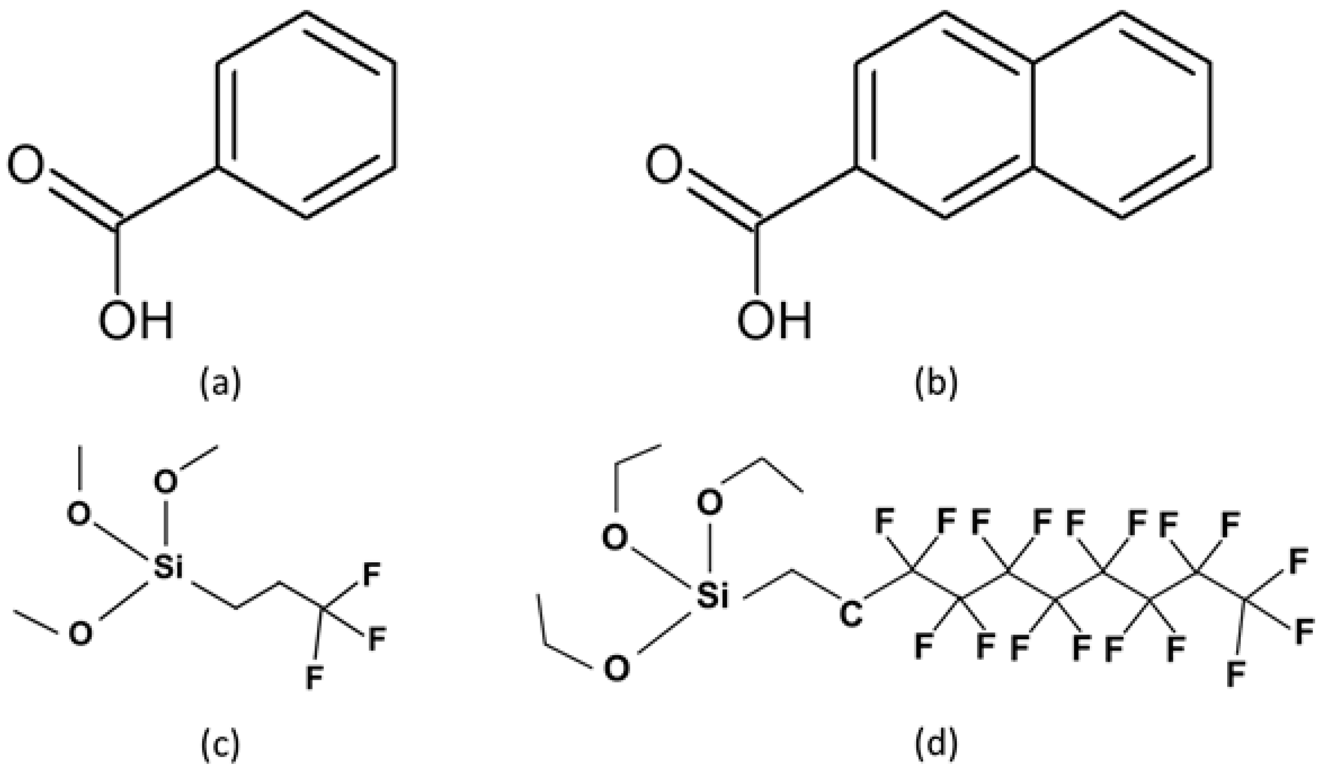
2. Materials and Modification

2.1. Materials

ITO used as the anode was purchased from AMG Co., Ltd. (Prides Crossing, MA, USA). The as-purchased ITO was deposited with a thickness of 150 ± 10 nm, with a sheet resistance value of ≤10 Ω/15 mm, and a transmittance of ≥85% at λ = 550 nm. The chemicals used to form the various SAMs—BA, NA, F-3SAM, and F-10SAM—were purchased from Gelest (BucksCounty, PA, USA).

2.2. Substrate Cleaning and Preparation

The ITO substrates were first cleaned to facilitate effective SAM deposition. A sequence of ultrasonic cleaning steps was performed using, in order, ultra-pure water, acetone, ultra-pure water, and 2-propanol for 5 min each. The ITO substrates were then dried on a hot plate at 150 °C for 5 min to remove moisture. The dried ITO substrates were then subjected to UV–ozone treatment for 20 min.

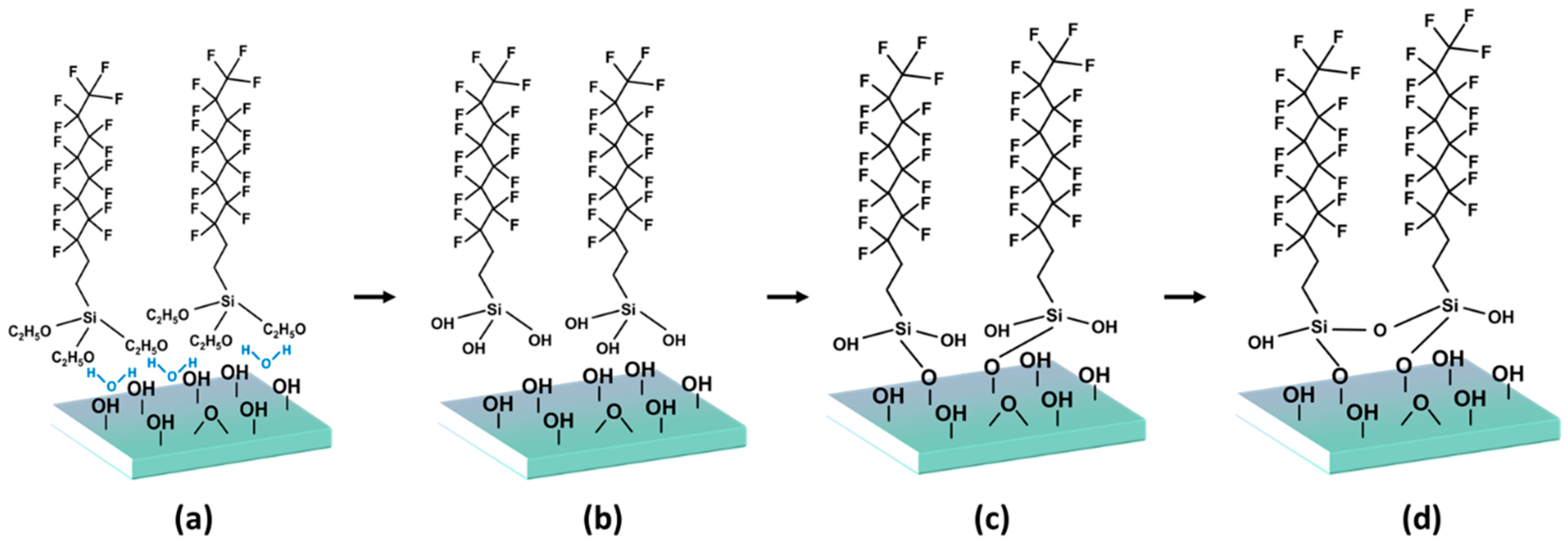
2.3. SAM Modification of the ITO Surface

In this study, four types of SAMs were prepared using BA, NA, F-3SAM, and F-10SAM. Figure 1 shows the SAM precursor molecules. A dipping process was employed to deposit a SAM onto the surface of the ITO substrate. To prepare the solution for the dipping process, 2 mM of each SAM precursor and 100 mL of ethanol were mixed with a stirrer at 300 RPM for 20 min. The washed ITO substrates were dipped in the solutions and left at room temperature for 72 h. The modified ITO was subjected to ultrasonic cleaning in 2-propanol for 5 min and then placed on a hot plate at 150 °C for 5 min. The contact angle was measured by a contact angle analyzer from Surface tech (GSX) (Chowol, Gwanju, Gyeonggi-do, Korea), in a Sessile drop mode, and the average roughness was measured by a scanning probe microscope from Park Systems (NX20) (KANC, Gwanggyo, Suwon, Korea), and the work function was measured by a Hitachi High Tech (AC-2) photoelectron spectrometer (Hitachi Inc., Tokyo, Japan).

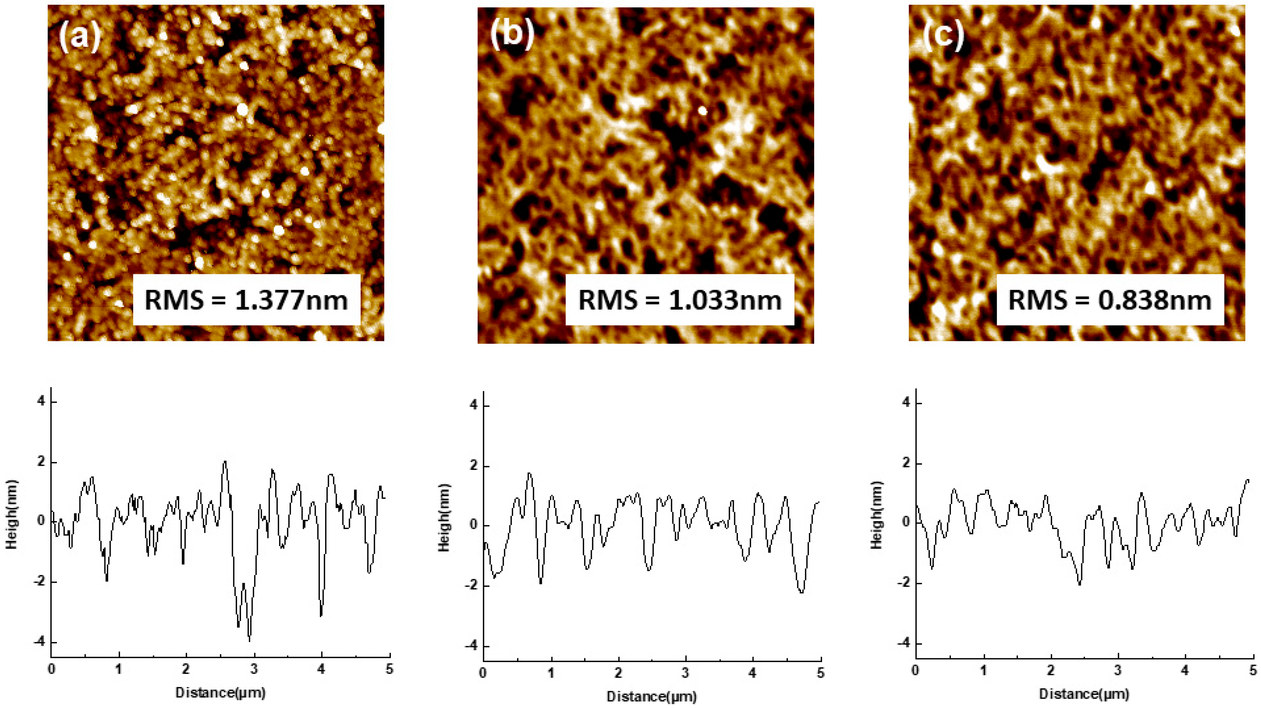
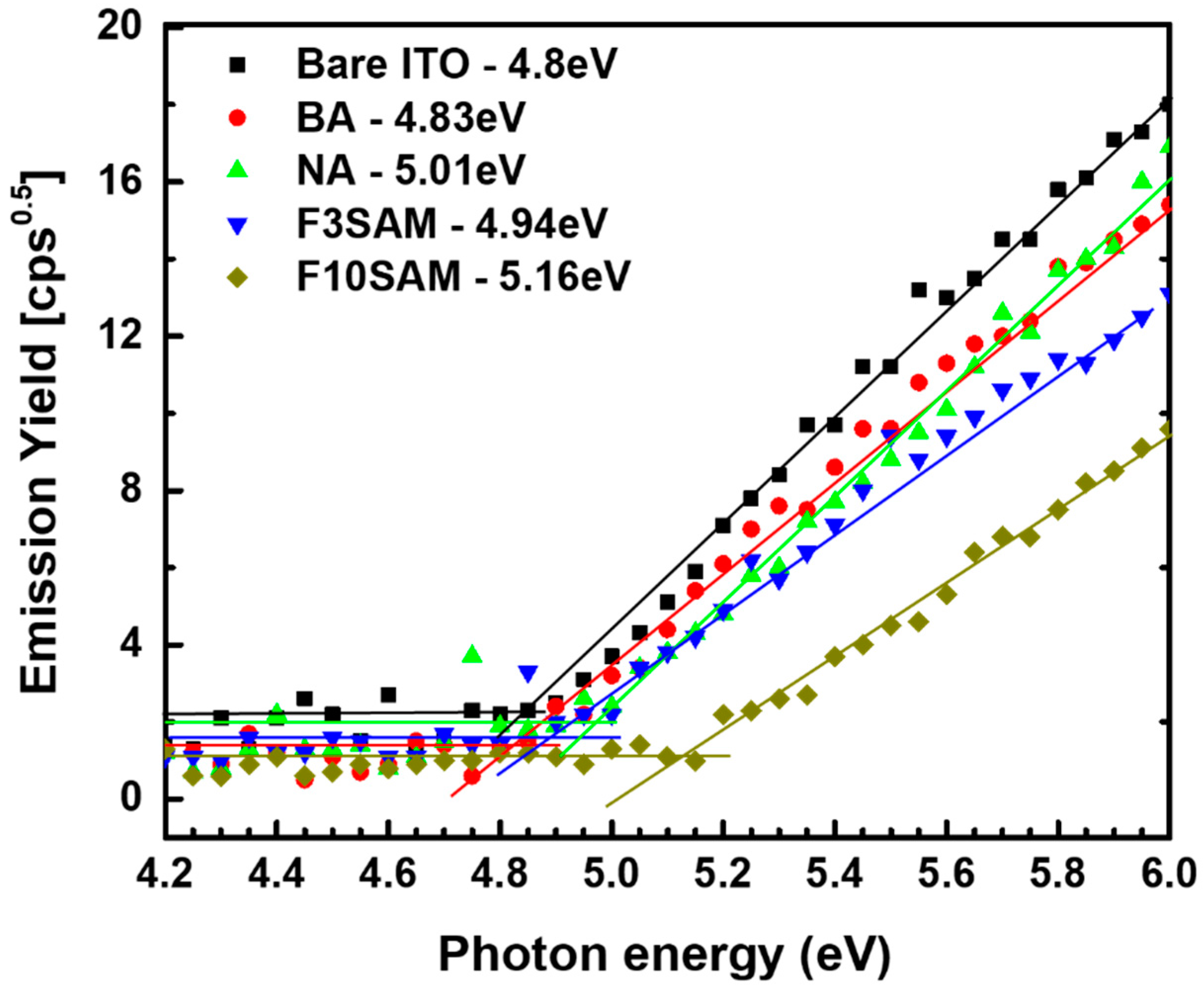
3. Results and Discussion

The SAM formation proceeds according to the following steps: first, a low-density layer is formed, which shows fluidity due to low surface coverage; an intermediate-density layer comprising an uneven condensation of molecules then develops; after the degree of SAM coverage reaches a threshold value, these molecules align horizontally on the surface; finally, when the SAM achieves a high density on the surface, a rearrangement of the SAM molecules occurs along the vertical direction, forming a well-aligned SAM [8].
Water plays an important role in the SAM formation mechanism. A thin layer of water is present on the surface of the ITO substrate, which is physically adsorbed by the SAM. The alkyl group of the physically adsorbed SAM has fluidity, which helps align the SAM by the van der Waals force between the alkyl groups before condensation occurs [18,19,20]. The aliphatic SAM is hydrolyzed by water, and it obtains a hydroxyl group, which reacts with the hydroxyl groups present on the surface of the ITO substrate to form an Si–O alkyl group bond; the hydroxyl groups that do not react with the surface lose water through a condensation reaction, resulting in a polymerization reaction and an Si–O–Si bond. Thus, a well-aligned SAM is formed by strong bonding between the SAM and the substrate surface; the mechanism is shown in Figure 2. In the case of aromatic SAM, chemical bonding with the surface of ITO was achieved through dehydration condensation reaction between carboxyl group and hydroxyl groups.
Contact angles were measured to confirm whether the different SAMs were successfully adsorbed onto the ITO substrate and to observe the change in surface properties. The results are shown in Figure 3 and Figure 4, which show the measurement results of the contact angles of the ITO substrates modified by the different SAMs. The measurement results were 41.1°, 61.7°, 82.25°, 78.2°, and 118° for bare ITO, BA, NA, F-3SAM, and F-10SAM, respectively. This result could be due to the energy level becoming lower as the number of π electrons increases in the π-conjugated system of the aromatic ring structure, and thus, as the length of conjugation increases [21,22]. In contrast, for the aliphatic SAM, the formation of a denser SAM on the ITO surface may have resulted from the strong van der Waals interaction between the alkyl chains as the alkyl chain length increased. The results show that for each SAM the precursors had successfully adsorbed onto the ITO surface and also that the modified surface has low wettability, displaying hydrophobicity. In theory, holes are injected into the HTM through the ITO surface. ITO is a hydrophilic inorganic surface. In contrast, HTM is a hydrophobic organic material. This difference induces a heterojunction between the two interfaces, adversely affecting the growth and stability of the organic film [23]. This increases the hydrophobicity of the surface through the formation of the SAM on the ITO surface, thus eliminating the inorganic/organic imbalance at the ITO/HTM interface.
The contact angle results for the various SAMs show different results depending on the aromatic ring structure and the aliphatic molecular structure. For the aromatic ring structure, it was confirmed that the contact angle increased as the number of aromatic rings increased; for the aliphatic molecular structure, the contact angle increased as the chain length increased.
These results indicate that the ITO interface had a higher contact angle when the aliphatic alkyl chain length was increased than when the number of aromatic rings was increased. This can be expressed as a quantitative ratio through Cassie’s law, which is shown below.
cos θ = ( 1 C 1 ) cos θ 1 + C 1 cos θ 2
When C1 has a value between 0 and 1, θ1 is the contact angle of bare ITO, and θ2 is the contact angle of the ITO surface modified by F-10SAM in the above equation, the quantitative ratio of SAMs based on Cassie’s law is shown in Figure 4. The ratios are 0% for bare ITO, 34.3% for BA, 73.7% for NA, 44.8% for F-3SAM, and 100% for F-10SAM. This equation confirms that for different SAM-modified ITO surfaces, higher hydrophobicity was exhibited when the aliphatic chain length was increased than when the number of aromatic rings was increased.
Figure 5 and Table 1 show the atomic force microscope images and the average roughness values from measurement results on bare ITO, the aromatic-NA-modified ITO surface, and the aliphatic-F-10SAM-modified ITO surface. The average roughness effective values measured by an atomic force microscope were as follows: bare ITO, 1.377 nm; NA, 1.033 nm; and F-10SAM, 0.838 nm. These AFM results show that the average roughness of the SAM-modified ITO is reduced, both of which show a similar surface topology indicating one or more single monolayers of SAM molecules have been formed on the ITO surface [24,25]. The low average roughness and hydrophobicity of the ITO surface could resolve the energy difference between ITO and the HTM.
ITO has a low work function value of approximately 4.8 eV. The low work function value of ITO induces a large energy barrier due to the difference with the large work function of HTM materials, resulting in a low hole injection efficiency. Figure 6 shows the graph of the work function measurement results when the SAMs are modified on the ITO surface by ultraviolet photoelectron spectroscopy. The measurement results were 4.83, 5.01, 4.94, and 5.16 eV for BA, NA, F-3SAM, and F-10SAM, respectively, which show that the work function value of the ITO surface increases through SAM film modification. Furthermore, these results have confirmed that the work function shifts to higher values for the aliphatic-structure SAM-modified surface than for the aromatic-ring-structure SAM-modified surface.
The large work function value of the ITO surface reduces the difference of the work functions between the HTM material and the ITO electrode to facilitate hole injection, thus improving the efficiency of the OLED device.

4. Conclusions

This study investigated the surface properties of aromatic-ring- and aliphatic-structured SAMs used to modify ITO substrates. The measured contact angles were 41.1°, 82.25°, and 118° for the bare ITO, NA, and F-10SAM, respectively, indicating that the contact angle and hydrophobicity increased for the ITO modified with F-10SAM. Moreover, the average roughness of the SAM-modified surfaces were 1.377, 1.033, and 0.838 nm for the bare ITO, NA, and F-10SAM, respectively, indicating that the SAMs decreased the surface roughness of ITO. The work function of the ITO surface modified with NA and F-10SAM increased from 0.21 eV and 0.36 eV to 5.01 and 5.16 eV, respectively. According to the results of this study, ITO was better improved when aliphatic SAM was deposited than when an aromatic-ring SAM was deposited. This is attributed to the fact that the energy level decrease due to the strong van der Waals interaction between alkyl chains of aliphatic SAM is greater than the energy level decrease due to the conjugated length of the aromatic SAM system. The study confirmed that the interfacial properties of ITO are improved when the ITO surface is modified by a SAM.

Author Contributions

Conceptualization, J.-E.S.; methodology, J.-E.S.; validation, S.-G.P.; formal analysis, M.-G.B.; investigation, M.-G.B.; resources, J.-E.S.; data curation, M.-G.B.; writing—original draft preparation, M.-G.B.; writing—review and editing, S.-G.P.; visualization, M.-G.B.; supervision, S.-G.P.; project administration, S.-G.P.; funding acquisition, J.-E.S. All authors have read and agreed to the published version of the manuscript.

Funding

This work was supported by the Korea Institute of Energy Technology Evaluation and Planning (KETEP) and the Ministry of Trade, Industry, and Energy (MOTIE) of the Republic of Korea (project no. 20173010013680).

Institutional Review Board Statement

Not applicable.

Informed Consent Statement

Not applicable.

Conflicts of Interest

The authors declare no conflict of interest.

References

  1. Ji, S.-B.; Choi, H.-W.; Yook, S.-K. Materials for Organic Light Emitting Diodes. Korean Ind. Chem. News 2016, 19, 1–11. [Google Scholar]
  2. Guillén, C.; Herrero, J. TCO/metal/TCO structures for energy and flexible electronics. Thin Solid Film. 2011, 520, 1–17. [Google Scholar]
  3. Tak, Y.H.; Kim, K.B.; Park, H.G.; Lee, K.H.; Lee, J.R. Criteria for ITO (indium–tin-oxide) thin film as the bottom electrode of an organic light emitting diode. Thin Solid Film. 2002, 411, 12–16. [Google Scholar]
  4. Lee, H.; Lee, D.; Ahn, Y.; Lee, E.W.; Park, L.S.; Lee, Y. Highly efficient and low voltage silver nanowire-based OLEDs employing a n-type hole injection layer. Nanoscale 2014, 6, 8565–8570. [Google Scholar]
  5. Benor, A.; Takizawa, S.Y.; Pérez-Bolívar, C.; Anzenbacher, P., Jr. Efficiency improvement of fluorescent OLEDs by tuning the working function of PEDOT: PSS using UV–ozone exposure. Org. Electron. 2010, 11, 938–945. [Google Scholar]
  6. Kanno, H.; Holmes, R.J.; Sun, Y.; Kena-Cohen, S.; Forrest, S.R. White stacked electrophosphorescent organic light-emitting devices employing MoO3 as a charge-generation layer. Adv. Mater. 2006, 18, 339–342. [Google Scholar]
  7. Li, L.; Guan, M.; Cao, G.; Li, Y.; Zeng, Y. Low operating-voltage and high power-efficiency OLED employing MoO3-doped CuPc as hole injection layer. Displays 2012, 33, 17–20. [Google Scholar]
  8. Sung, M.-M. Self-Assembled Monolayers, SAMs. Electron. Mater. Lett. 2007, 3, 137–145. [Google Scholar]
  9. Ulman, A. Formation and Structure of Self-Assembled Monolayers. Chem. Rev. 1996, 96, 1533–1554. [Google Scholar]
  10. Chi, Y.S.; Kang, S.M.; Choi, I.S. Surface Engineering Based on Self-Assembled Monolayers. Polym. Sci. Technol. 2006, 17, 172–181. [Google Scholar]
  11. Ulman, A. An Introduction to Ultrathin Organic Films; Academic Press: Boston, MA, USA, 1991. [Google Scholar]
  12. Chaki, N.K.; Vijayamohanan, K. Self-assembled monolayers as a tunable platform for biosensor applications. Biosens. Bioelectron. 2002, 17, 1–12. [Google Scholar] [PubMed]
  13. Yip, H.L.; Hau, S.K.; Baek, N.S.; Ma, H.; Jen, A.K.Y. Polymer solar cells that use self-assembled-monolayer-modified ZnO/metals as cathodes. Adv. Mater. 2008, 20, 2376–2382. [Google Scholar]
  14. Park, S.G.; Park, H.G. Alignment of liquid crystal molecules on self-assembled monolayer with fluorinated alkyl chain at different deposition time. Opt. Mater. 2018, 85, 298–302. [Google Scholar]
  15. Yan, L.; Huck, W.T.S.; Whitesides, G.M. Self-Assembled Monolayers (SAMs) and Synthesis of Planar Microand Nanostructures. J. Macromol. Sci. Part C 2004, 44, 175–206. [Google Scholar]
  16. Sharma, A.; Hotchkiss, P.J.; Marder, S.R.; Kippelen, B. Tailoring the work function of indium tin oxide electrodes in electrophosphorescent organic light-emitting diodes. J. Appl. Phys. 2009, 105, 084507. [Google Scholar]
  17. Wang, M.; Hill, I.G. Fluorinated alkyl phosphonic acid SAMs replace PEDOT: PSS in polymer semiconductor devices. Org. Electron. 2012, 13, 498–505. [Google Scholar]
  18. Wasserman, S.R.; Tao, Y.T.; Whitesides, G.M. Structure and reactivity of alkylsiloxane monolayers formed by reaction of alkyltrichlorosilanes on silicon substrates. Langmuir 1989, 5, 1074–1087. [Google Scholar]
  19. Silberzan, P.; Leger, L.; Ausserré, D.; Benattar, J.J. Silanation of silica surfaces. A new method of constructing pure or mixed monolayers. Langmuir 1991, 7, 1647–1651. [Google Scholar]
  20. Allara, D.L.; Parikh, A.N.; Rondelez, F. Evidence for a Unique Chain Organization in Long Chain Silane Monolayers Deposited on Two Widely Different Solid Substrates. Langmuir 1995, 11, 2357–2360. [Google Scholar]
  21. Ajayaghosh, A. Donor–acceptor type low band gap polymers: Polysquaraines and related systems. Chem. Soc. Rev. 2003, 32, 181–191. [Google Scholar]
  22. Van Mullekom, H.A.M. The Chemistry of High and Low Band Gap Pi-Conjugated Polymers; Technische Universiteit Eindhoven: Eindhoven, The Netherlands, 2000. [Google Scholar]
  23. Donley, C.L.; Dunphy, D.R.; Doherty, W.J.; Zangmeister, R.; Drager, A.S.; O’Brien, D.F.; Saavedra, S.S.; Armstrong, N.R. Indium—Tin Oxide Organic Interfaces; American Chemical Society (ACS): Washington, DC, USA, 2003; Volume 844, pp. 133–153. [Google Scholar]
  24. Park, Y.; Choong, V.; Gao, Y.; Hsieh, B.R.; Tang, C.W. Work function of indium tin oxide transparent conductor measured by photoelectron spectroscopy. Appl. Phys. Lett. 1996, 68, 2699–2701. [Google Scholar] [CrossRef]
  25. Mermer, O.; Asci, Y. Enhancement of optical and electrical performance of organiclight emitting diodes fabricated by SAM modified ITO anodes. J. Optoelectron. Adv. Mater. 2015, 17, 1339–1343. [Google Scholar]
Figure 1. Molecular structures of the self-assembled monolayer (SAM) precursors (a) benzoic acid (BA), (b) 2-naphthoic acid (NA), (c) (3,3,3-trifluoropropyl)trimethoxysilane (F-3SAM), and (d) (heptadecafluoro-1,1,2,2-tetrahydrodecyl)triethoxysilane (F-10SAM).
Crystals 11 00026 g001
Figure 2. SAM formation of process. SAM is formed through (a) physisorption, (b) hydrolysis, (c) covalent grafting to the substrate, and (d) in plane reticulation.
Crystals 11 00026 g002
Figure 3. Contact angle measurement of the indium tin oxide (ITO) substrates with different treatments (a) bare ITO, (b) BA, (c) NA, (d) F-3SAM, and (e) F-10SAM.
Crystals 11 00026 g003
Figure 4. Contact angle measurement result and coverage quantitative ratio.
Crystals 11 00026 g004
Figure 5. Average roughness, as determined by atomic force microscopy (AFM), for (a) ITO, (b) NA, and (c) F-10SAM.
Crystals 11 00026 g005
Figure 6. Work function of BA, NA, F-3SAM, and F-10SAM.
Crystals 11 00026 g006
Table 1. Results of the roughness values (Mean—Mean line; Rpv—R peak to peak value, Rq—R root mean square, Ra—R average, and Rz—ten-point height).
RegionMinMaxMidMeanRpvRqRaRz
ITO−5.26115.1974.9680.07720.4581.3771.01818.536
NA−5.2015.4050.102010.6061.0330.8069.414
F10SAM−4.6494.9040.12809.5530.8380.6578.988
Publisher’s Note: MDPI stays neutral with regard to jurisdictional claims in published maps and institutional affiliations.

