Article

Controlling Spontaneous Emission from Perovskite Nanocrystals with Metal–Emitter–Metal Nanostructures

1
CINTRA (CNRS-International-NTU-THALES Research Alliances/UMI 3288), Research Techno Plaza, 50 Nanyang Drive, Border X Block, Level 6, Singapore 637553, Singapore
2
School of Electrical and Electronic Engineering, Nanyang Technological University, 50 Nanyang Avenue, Singapore 639798, Singapore
3
Energy Research Institute @ NTU (ERIAN), Research Techno Plaza, 50 Nanyang Drive, X-Frontiers Block, Level 5, Singapore 637553, Singapore
*
Authors to whom correspondence should be addressed.
Crystals 2021, 11(1), 1; https://doi.org/10.3390/cryst11010001
Submission received: 5 November 2020 / Revised: 17 December 2020 / Accepted: 21 December 2020 / Published: 22 December 2020

Abstract

:
We show the increase of the photoluminescence intensity ratio (PLR) and the emission rate enhancement of perovskite cesium lead bromide (CsPbBr3) and formamidinium lead bromide (FAPbBr3) nanocrystals (NCs) in the presence of single and double gold layer cavities, which we refer to as Metal-Emitter (ME) and Metal-Emitter-Metal (MEM) nanostructures. Up to 1.9-fold PLRs and up to 5.4-fold emission rate enhancements were obtained for FAPbBr3 NCs confined by double gold layers, which are attributed to plasmonic confinement from the gold layers. The experimentally obtained values are validated by analytical calculations and electromagnetic simulations. Such an effective method of manipulation of the spontaneous emission by simple plasmonic nanostructures can be utilized in sensing and detection applications.

1. Introduction

Metal halide perovskites for quantum emitters have gained interest over the years due to their low cost and solution-processable characteristics [1]. Importantly, the defect-tolerant characteristics of halide perovskites are responsible for their high absorption coefficients and high photoluminescence (PL) quantum yield, enabling potential large-scale applications in photovoltaic (PV) devices [2], scintillators [3,4,5,6], light-emitting diodes (LEDs), lasers, photodetectors, and field-effect transistors (FETs) [7]. A moderate exciton binding energy in the several meV range, large oscillator strength, and tuneable bandgap achieved via tailoring of chemical composition and structural diversity are the other advantages of halide perovskite, notably in nonlinear optics applications [8] and strong light–matter interaction between the quantum emitter and optical cavity.
Coupling electromagnetic modes with a quantum emitter [9,10] results in the emission rate modification known as the Purcell effect, which is relevant for realizing single-photon nano-emitters [11]. The light-confining structures can be realized via different platforms, such as photonic crystals [12,13], disorder [14,15], and plasmonic nanostructures [16]. In this work, we investigate the spontaneous emission rate modification of halide perovskite nanocrystals (NCs) coupled with simple plasmonic cavities. The quantum emitters investigated in this work are cesium lead bromide (CsPbBr3) and formamidinium lead bromide (FAPbBr3) NCs, while the plasmonic cavity is defined in metal–emitter (ME) and metal–emitter–metal (MEM) structures in which the NCs are sandwiched between single and double gold films, respectively. We obtained 1.2-fold and 1.9-fold PL intensity ratios (PLR) for CsPbBr3 and FAPbBr3 NCs, respectively, whereas the emission rate enhancements are 4.3-fold and 5.4-fold for CsPbBr3 and FAPbBr3 NCs, respectively. Manipulation of the spontaneous emission rate by simple plasmonic nanostructures can be utilized in sensing and detection applications [17,18]. Furthermore, such simple structures with large emission enhancement factors will improve the brightness for light-emitting devices (LED) applications and improve the signal modulations in telecommunication technologies.

2. Materials and Methods

The schematic of the ME and MEM structures are shown in Figure 1a. The 100 nm thick bottom gold layer was physically deposited on glass substrate by electron beam evaporation. To avoid non-radiative losses, a thin polystyrene (PS) layer was deposited in between the gold and perovskite layer. The PS layer was spin coated from PS in toluene solution (1.5% w/v) at 8000 rpm to obtain initial thickness of 35 nm, followed by oxygen plasma etching (450 mBar, 30–50 s) to reach 15 nm thickness. CsPbBr3 NCs were synthesized according to a hot-injection protocol described in the literature [5,19]. In a typical synthesis, 0.7 g lead (II) bromide (PbBr2), oleic acid (0.5 mL), oleyl amine (0.5 mL) and octadecene (5 mL) were loaded into a 50 mL flask and dried under vacuum at 100 °C for 0.5 h. Subsequently, nitrogen (N2) was introduced and the mixture was heated up to 170 °C until PbBr2 was completely dissolved. A hot Cs-oleate precursor (0.5 mL) was quickly injected into the flask under vigorous stirring. After 10 s of reaction, the flask was quickly immersed into an ice bath to quench the reaction. The CsPbBr3 NC precipitate was collected by centrifugation for 10 min. The NC suspension was then spun on the cover slide at 4000 rpm for 10 s (for 100 nm thickness) and at 6000 rpm for 10 s (for 50 nm thickness) with initial volumes of 0.1 and 0.05 mL, respectively. FAPbBr3 NCs were synthesized and spin coated by methods described in Chin et al. [20].
PL measurements were performed at room temperature (RT) using free-space excitation and collection through a visible−near-infrared microscope objective (Nikon 20×, Nikon Corporation, Tokyo, Japan, NA = 0.40). The sample was excited via a 10 MHz picosecond pulsed diode laser (Master Oscillator Fibre Amplifier, Picoquant, Picoquant GmbH, Berlin, Germany, excitation wavelength at 355 nm, pulse width 50 ps, and power of 40 µW). The PL measurement was based on epifluorescence method. PL spectra were detected using AvaSpec-HERO spectrometer (Avantes BV, Apeldoorn, The Netherlands). The emission was then filtered by a linear variable filter at 505 and 545 nm and detected by a single-photon avalanche photodiode connected to a time-correlated single-photon counting acquisition module (Edinburgh Instruments, TCC900, Edinburgh Instruments Ltd., Livingstone, United Kingdom). The time-resolved photoluminescence (TRPL) decay curves were fitted with two exponential functions. The average lifetime was calculated from the decay time components and amplitudes of the fitted TRPL decay curves.
For the double gold structure, another gold layer was evaporated on another PS layer on top of the perovskite NC layer to 100 nm thickness. The scanning electron micrograph (SEM) of the double gold structure is shown in Figure 1b, with each layer indicated accordingly. The thicknesses of the layers are verified from Scanning Electron Microscopy (SEM) images with the cross-section thicknesses analyzed statistically (an example is shown in Figure S1 in Supplementary Information). The transmission electron micrograph (TEM) pictures of the CsPbBr3 and FAPbBr3 NCs are shown in Figure 1c,d, respectively.

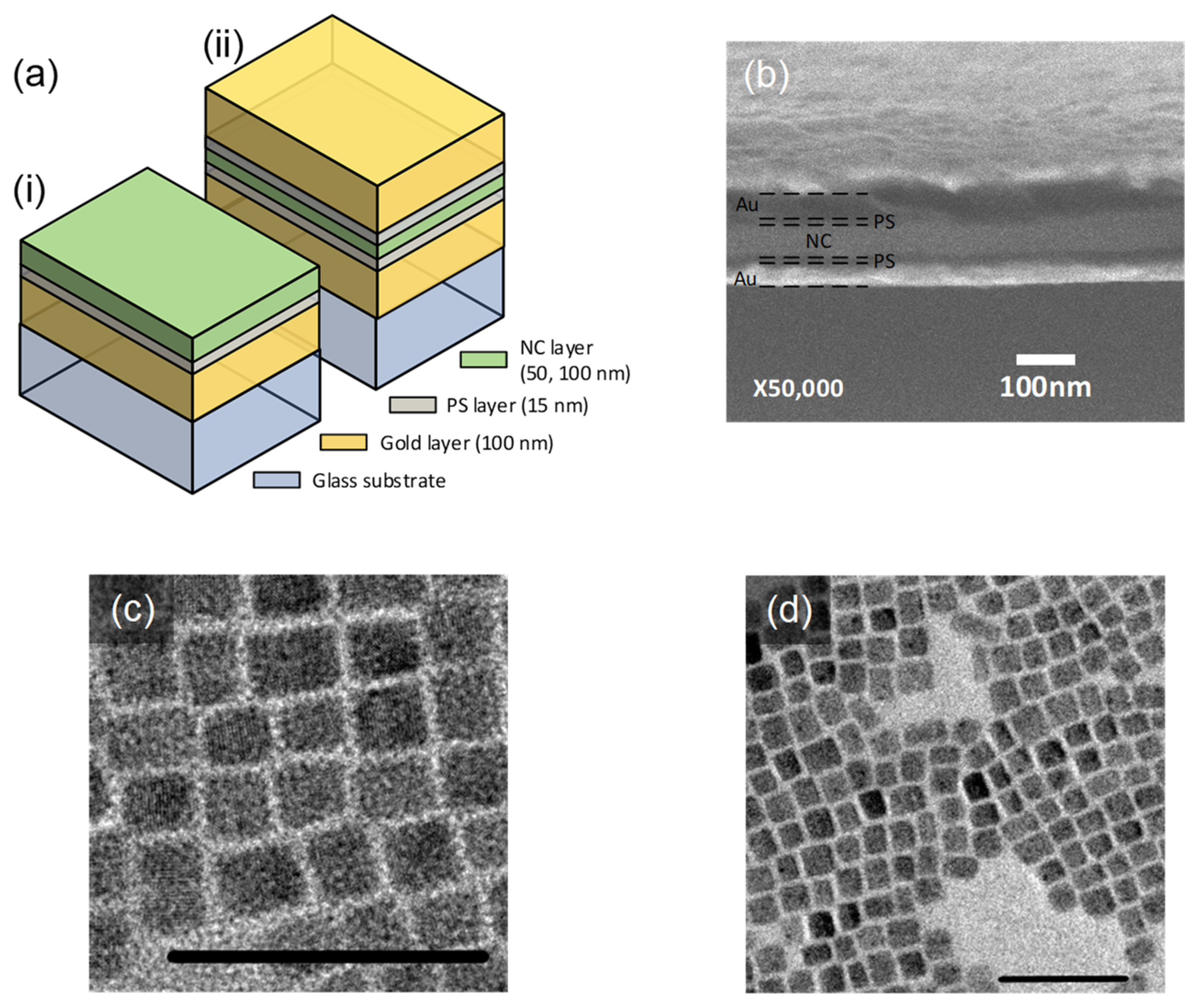
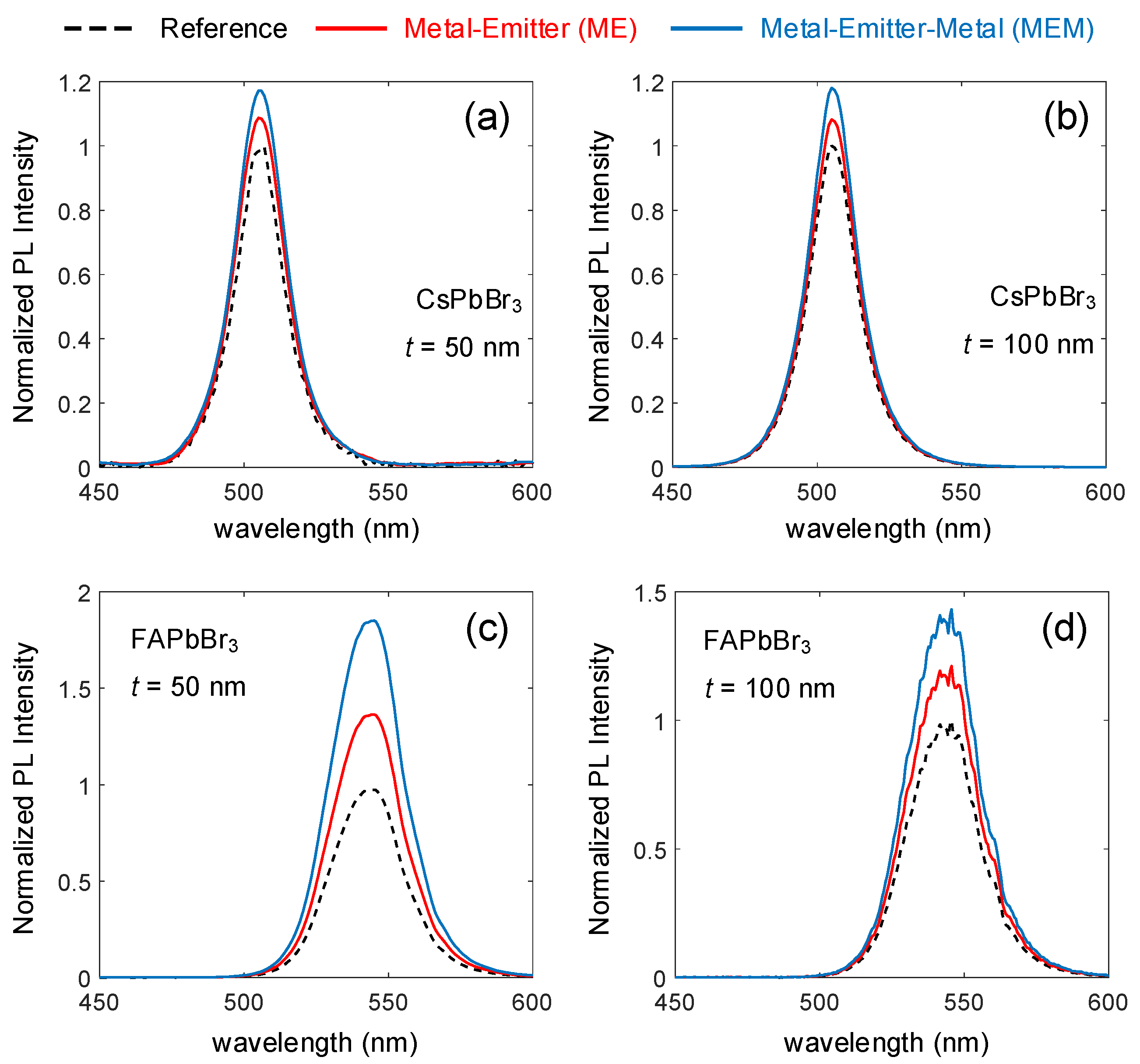
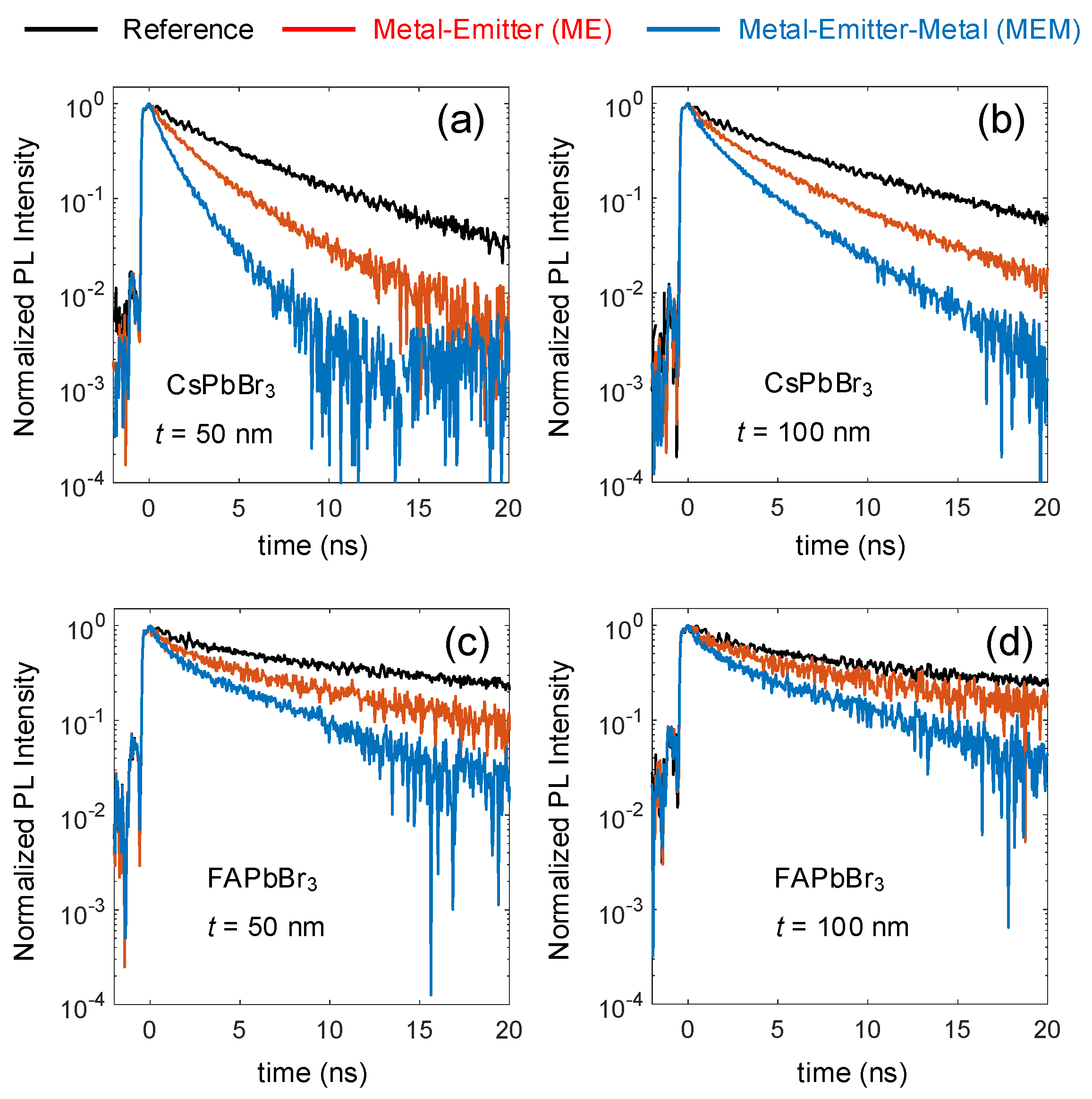
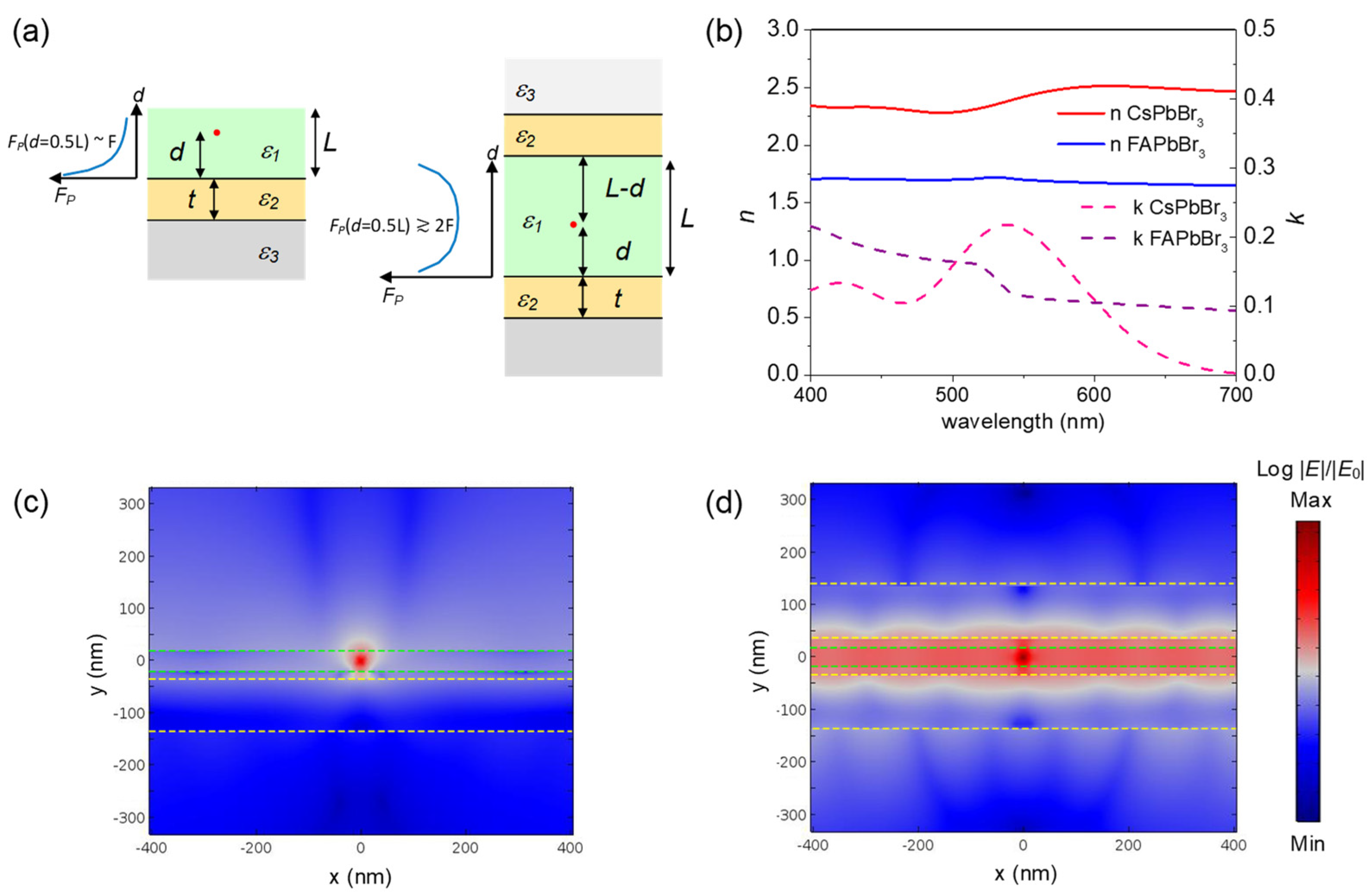
3. Results and Discussion

Figure 2 presents the PL spectra of CsPbBr3 and FAPbBr3 NCs in different scenarios. We varied the thickness of the NC layer to 50 and 100nm for the two NCs and normalized the PL spectra to those of the reference (dashed black curves). The reference is PS-NC-PS system (Figure S2 in Supplementary Information). The emission wavelengths are found at 505 nm (for CsPbBr3 NC) and 545 nm (for FAPbBr3 NC). For each experimental data point, the PL and TRPL measurements were performed at two positions of 5 mm apart on the same sample, and the average and standard deviation of the results were taken. We defined the PLR as the direct ratio between the measured PL intensity of ME or MEM structure, over the PL intensity of the reference sample, see Table 1. The normalized PL spectra of NCs in ME situation are shown in red curves, showing PLR of ~1.13 and ~1.41 times for CsPbBr3 and FAPbBr3 NCs of 50 nm thickness, respectively. Here, a 15 nm thick PS layer is introduced between the gold film and the NC layer to minimize non-radiative loss. The non-radiative loss associated with metals is commonly attributed to the energy transfer from excited electrons to the free carriers inside the metal. Inserting a thin insulating layer would reduce such non-radiative loss [21,22,23]. Stronger resonance is expected when a second gold layer is introduced. The resonance characteristics of ME and MEM structures were verified in the thickness-dependent peak positions in the transmittance measurement (see Figure S3 in Supplementary Information). Normalized PL spectra of NCs in metal–emitter–metal samples are shown in blue curves, showing PLR of ~1.23 (for CsPbBr3 NC) and ~1.91 (for FAPbBr3 NC) of 50 nm thickness.
It should be noted that, due to its top gold layer, the measured PLR for the MEM structure is not equivalent to its actual PL intensity enhancement (PLE). This is because the excitation power is first absorbed by the top gold layer before being absorbed by the perovskite NC thin film underneath. Furthermore, the PL emission from the perovskite NC thin film needs to pass through the same top gold layer before being detected in our experiment. Therefore, the transmittance of the top gold layer should be considered to calibrate the excitation power in the perovskite NC thin film. As discussed in the text following Figure S4 in Supplementary Information, the transmittance of the top gold layer at excitation wavelength, i.e., T g ( λ = 355 n m ) , can be deduced as T g ( λ = 355 n m ) = 0.0725 . The PLE for the MEM structure can thus be estimated as ≳16.3 for 100 nm thick CsPbBr3. The scope of this work, however, is more on the direct measurements of PLR of ME and MEM structures, with respect to the PL intensity of the reference sample.
As both the gold film(s) and the NC layer form the plasmonic cavity, with light confinement within the NC layer, the role of the NC layer is thus expected on the resonance condition. This is illustrated when the NC layer thickness is increased to 100 nm, presented in 2b, d for CsPbBr3 and FAPbBr3 NCs, respectively. While the PLR remains relatively unchanged for CsPbBr3 NCs, it decreases from ~1.41 to ~1.21 (for ME configuration) and from ~1.91 to ~1.42 (for the metal–emitter–metal configuration) for FAPbBr3 NCs. By the same reasoning, the resonance condition is also dependent on the thickness of the PS spacer layer. This means that the PS layer serves not only to minimize non-radiative loss, but also to modify the resonance condition of the plasmonic cavity. The PL characteristics of NC layer without PS spacer layer is shown in Figure S5 (Supplementary Information), indicating strong decrease in emission intensity, which has also been observed before [24]. TRPL characteristics for all scenarios are presented in Figure 3, showing spontaneous emission rate modification as the NCs are coupled in ME or MEM configurations. Since both intensity and emission rate are enhanced, as shown in Table 1, this indicates the Purcell effect taking place in both types of NCs. To verify the role of PS spacer layer in Purcell effect, we present in Figure S6 (Supplementary Information) the TRPL measurements of 50 nm thick CsPbBr3 NCs on gold film without PS spacer layer. We found that the fast decay component in this situation is very close to the instrument response function (IRF) of about 0.3 ns [23]. Coupled with the intensity decrease in Figure S1, it is seen that the fast decay rate is not attributed to Purcell effect, but to non-radiative loss instead. Therefore, while there is a reduction of non-radiative recombination by PS, the plasmonic/dielectric cavities are still the key driving force which enhances the emission rate.
To further understand the experimental results, we turn to analytical calculation and then validate it with finite element simulation (FEM) in COMSOL. The ME and MEM configurations can be modelled as a set of thin-film stacks with different optical permittivity values and the NCs as dipoles within the NC layer, as denoted by the red dots, as shown in Figure 4a. The orientation of the electric dipole is such that it gives emission in the XY plane. Using the Fresnel reflections, the spontaneous emission rate modification of a dipole in ME configuration can be calculated as [25,26,27,28]
F P = Γ T Γ 0 = 1 3 2 Q e   Im   0 R p 1 , 2 , 3 ( k 2 , t ) exp ( 2 l 1 d ) u 3 l 1 d u ,
where F P is the spontaneous emission rate enhancement factor, Q e is the quantum efficiency, d is the dipole distance from the interface of metal layer, t is the thickness of the metal layer, k is the propagation constant, l m = i ϵ m / ϵ 1 u 2 , R p 1 , 2 , 3 is the total p-polarized reflection from the thin film stack
R p 1 , 2 , 3 ( k 2 , t ) = R p 1 , 2 + ( R p 2 , 3 . e 2 l 2 k 2 t ) 1 + R p 1 , 2 . ( R p 2 , 3 . e 2 l 2 k 2 t ) ,
with R p m , n = ϵ m l n ϵ n l m ϵ m l n + ϵ n l m denoting p-polarized Fresnel reflection between m- and nth layer. Subscripts 1, 2, and 3 refers to perovskite NC layer, gold layer, and glass substrate, respectively. For an electric dipole in the metal–emitter–metal configuration, the emission rate modification, F P = Γ T / Γ 0 , is
F P = 1 [ Q e . ( 1 3 2   Im 0 ( 1 R p 1 , 2 , 3 ( k 2 , t ) e 2 l 1 k 1 d ) ( 1 R p 1 , 2 , 3 ( k 2 , t ) e 2 l 1 k 1 ( L d ) ) ( 1 ( R p 1 , 2 , 3 ( k 2 , t ) ) 2 e 2 l 1 k 1 L ) u 3 l 1 d u ) ] ,
where the subscripts 1, 2, and 3 refers to perovskite NC layer, gold layer, and air, respectively.
The graphs next to the schematics in Figure 4a illustrate the change in spontaneous emission rate enhancement over dipole distance from metal surface. At the center of the perovskite film (d = 0.5 L), the spontaneous emission rate enhancement factor (FP) for double gold layer structure is approximately two times of that of the single gold case, in the range of L ≲ 0.5λ. The quantum efficiency of the perovskite NCs is assumed to be Q e = 0.4 [19,20], while their permittivity values were obtained from spectroscopic ellipsometry, as shown in Figure 4b. We note that the refractive index values of the FAPbBr3 appear to be lower than others reported elsewhere. This is attributed to the organic ligands protecting the surface of FAPbBr3 NCs, which makes it behave more like a composite rather than a thin-film crystal [20].
In the finite element simulation [23,29], the emission rate enhancement is calculated as the dipole power ratio between that within the plasmonic layer structures and that in the perovskite film only. The calculated |E|-field mappings at resonances for ME and MEM structures with CsPbBr3 NC film are shown in Figure 4c,d, respectively. The resonant wavelengths were found from simulation to be at 540 and 606 nm for ME and MEM structures, respectively. The resonant wavelength is the optical characteristic of the layer structure, obtained from FEM simulation, which is not related to the emission wavelength of the NCs, although ideally the emission and resonant wavelengths should coincide so that the final enhancement is at maximum. In addition, the peaks and the long wavelength shifts of the resonances from 50 and 100 nm MEM structures agree well with the transmittance measurements of Figure S3 in Supplementary Information. The NC layer is denoted by the green dashed lines, while the gold films are indicated by the yellow dashed lines. The optical modes are confined differently in the two configurations. The E-field for the ME case is localized at the vicinity of the electric dipole, while the E-field for the MEM case is rather extended in the transverse direction, mimicking that of a waveguide. This translates to stronger light-matter interaction in the MEM case, which gives higher emission rate modification.
The comparison among the calculated, simulated, and measured emission rates for the two NCs with 50 and 100 nm thicknesses is presented in Figure 5. For the calculation and FEM simulation in this work, the emission rate is averaged over more than 10 equally spaced points over the entire perovskite NC layer thickness. We found that our analytical results and FEM simulations are in good agreement with our experimental results. The difference is due to the boundary problem between PS and NC layers in both simulations. For FAPbBr3 NCs, up to 1.9-fold PLR and up to 5.4-fold emission rate enhancements were observed for the case of 50 nm thick NC layer in the double gold layer structure.
We note that PLR of FAPbBr3 NCs is higher than that of CsPbBr3 NCs. This can be attributed to the inter-band transition of gold at 539 nm [30,31], suggesting that the gold layer behaves more as dielectric at wavelengths shorter than its inter-band transition. Indeed, this appears to be the case for CsPbBr3 NCs whose emission wavelength is at 505 nm (<539 nm). However, the light is still confined by virtue of total internal reflection. This is because the real refractive index of gold is 0.887 at 505 nm [30]. Considering the real refractive index of CsPbBr3 NCs is 2.3 at 505 nm, the index contrast of ~1.4 is large enough for ensuring optical confinement within the NC layer. Considering the ~20 nm emission linewidth of CsPbBr3 NCs, the increase in PLR is attributed more to dielectric confinement rather than plasmonic confinement. This is in contrast with FAPbBr3 NCs, whose emission wavelength (545 nm) is longer than the inter-band transition of gold. Considering its emission linewidth of ~30 nm, the light confinement is dominated more by plasmonic mechanism rather than by total internal reflection. This also agrees with more pronounced increase in PLR in FAPbBr3 NCs compared to CsPbBr3 NCs.

4. Conclusions

The intensity and emission rate characteristics of CsPbBr3 and FAPbBr3 NCs have been investigated in two ME configurations. Owing to their emission wavelengths with respect to the inter-band transition of gold, the emission rate enhancements in the two NCs are attributed to different mechanisms. For CsPbBr3 NCs, whose emission wavelength is shorter than gold inter-band transition, the gold behaves more as dielectric and the light is confined by virtue of strong index contrast. For FAPbBr3 NCs, whose emission wavelength is longer than gold inter-band transition, the light is confined by plasmonic mechanisms. These confinement mechanisms are the reason for the big differences in the PL intensity increases and emission rate enhancements of the two NCs. By treating the ME and MEM configurations as thin film stacks, we arrived at the analytical formulation to elucidate the emission rate enhancement, which was also validated by our FEM simulation. We found good agreement between our calculation and our experimental results. In addition, we have shown that a simple plasmonic cavity based on single or double gold films can be used as a platform to study light-matter interaction, particularly in solution-processable perovskite NCs, which can be used for sensing application [17,18].
Other metals can be explored in the future. Silver should perform better compared to gold due to its much lower damping loss and its inter-band transition at the ultraviolet spectrum. However, unlike gold, silver is known to suffer from surface oxidation, which deteriorates its plasmonic response with time. The other good candidate is aluminum (Al), which is known to support plasmonic resonance in the UV-Vis spectrum. Moreover, its surface oxidation is known to be self-limiting in the 2–3 nm thickness range, which can also serve to minimize non-radiation loss as the PS layer in our work. Although Al damping loss is known to be higher than gold or silver, Al is an excellent candidate for plasmonics in the ultraviolet spectrum, making it suitable platform for quantum emitter in the short-visible wavelength range.

Supplementary Materials

The following are available online at https://www.mdpi.com/2073-4352/11/1/1/s1, Figure S1: Example of statistical analysis of layer thickness; Figure S2: Schematic of reference sample in PL and TRPL measurements, Figure S3: Transmittance of ME and MEM structures; Figure S4: Transmission and absorbance of ME and MEM structures; Figure S5: PL spectra of CsPbBr3 NC-Au layers (without PS) at RT; Figure S6: TRPL decay curves of CsPbBr3 NC film with Au, Table S1: Key parameters of time resolved PL spectrum.

Author Contributions

Conceptualization, M.D.B.; formal analysis, M.D.B., L.T. and L.Y.M.T.; investigation, M.D.B. and L.T.; resources, K.L., G.W.P.A. and X.Y.C.; data curation, M.D.B. and L.T.; writing—original draft preparation, M.D.B. and L.T.; writing—review and editing, L.Y.M.T. and G.W.P.A.; visualization, M.D.B., L.T. and L.Y.M.T.; supervision M.D.B., H.W. and D.H.Z. All authors have read and agreed to the published version of the manuscript.

Funding

This research was funded by Ministry of Education, Singapore, grant nos. MOE2016-T2-1-052 and MOE2019-T1-002-063.

Acknowledgments

We acknowledge Aozhen Xie for assistance in CsPbBr3 NC synthesis.

Conflicts of Interest

The authors declare no conflict of interest.

References

  1. Dai, X.; Zhang, Z.; Jin, Y.; Niu, Y.; Cao, H.; Liang, X.; Chen, L.; Wang, J.; Peng, X. Solution-Processed, High-Performance Light-Emitting Diodes Based on Quantum Dots. Nature 2014, 515, 96–99. [Google Scholar] [CrossRef] [PubMed]
  2. Abate, A.; Correa-Baena, J.P.; Saliba, M.; Su’ait, M.S.; Bella, F. Perovskite Solar Cells: From the Laboratory to the Assembly Line. Chem. A Eur. J. 2018, 24, 3083–3100. [Google Scholar] [CrossRef] [PubMed]
  3. Birowosuto, M.D.; Cortecchia, D.; Drozdowski, W.; Brylew, K.; Lachmanski, W.; Bruno, A.; Soci, C. X-Ray Scintillation in Lead Halide Perovskite Crystals. Sci. Rep. 2016, 6, 37254. [Google Scholar] [CrossRef] [PubMed] [Green Version]
  4. Xie, A.; Nguyen, T.H.; Hettiarachchi, C.; Witkowski, M.E.; Drozdowski, W.; Birowosuto, M.D.; Wang, H.; Dang, C. Thermal Quenching and Dose Studies of X-Ray Luminescence in Single Crystals of Halide Perovskites. J. Phys. Chem. C 2018, 122, 16265–16273. [Google Scholar] [CrossRef]
  5. Chen, Q.; Wu, J.; Ou, X.; Huang, B.; Almutlaq, J.; Zhumekenov, A.A.; Guan, X.; Han, S.; Liang, L.; Yi, Z.; et al. All-Inorganic Perovskite NC Scintillators. Nature 2018, 561, 88–93. [Google Scholar] [CrossRef] [PubMed]
  6. Birowosuto, M.D.; Dorenbos, P.; van Eijk, C.W.E.; Krämer, K.W.; Güdel, H.U. Güdel. Scintillation and Luminescence Properties of Ce3+ Doped Ternary Cesium Rare-Earth Halides. Phys. Status Solidi A 2007, 204, 850–860. [Google Scholar] [CrossRef]
  7. Zhou, C.; Lin, H.; He, Q.; Xu, L.; Worku, M.; Chaaban, M.; Lee, S.; Shi, X.; Du, M.H.; Ma, B. Low Dimensional Metal Halide Perovskites and Hybrids. Mater. Sci. Eng. R Rep. 2019, 137, 38–65. [Google Scholar] [CrossRef]
  8. Wu, L.; Chen, K.; Huang, W.; Lin, Z.; Zhao, J.; Jiang, X.; Ge, Y.; Zhang, F.; Xiao, Q.; Guo, Z.; et al. Perovskite Cspbx3: A Promising Nonlinear Optical Material and Its Applications for Ambient All-Optical Switching with Enhanced Stability. Adv. Opt. Mater. 2018, 6, 1800400. [Google Scholar] [CrossRef]
  9. Gholipour, B.; Adamo, G.; Cortecchia, D.; Krishnamoorthy, H.N.; Birowosuto, M.D.; Zheludev, N.I.; Soci, C. Organometallic Perovskite Metasurfaces. Adv. Mater. 2017, 29, 201604268. [Google Scholar] [CrossRef]
  10. Hou, S.; Xie, A.; Xie, Z.; Tobing, L.Y.; Zhou, J.; Tjahjana, L.; Yu, J.; Hettiarachchi, C.; Zhang, D.; Dang, C.; et al. Concurrent Inhibition and Redistribution of Spontaneous Emission from All Inorganic Perovskite Photonic Crystals. ACS Photonics 2019, 6, 1331–1337. [Google Scholar] [CrossRef]
  11. Hou, S.; Birowosuto, M.D.; Umar, S.; Anicet, M.A.; Tay, R.Y.; Coquet, P.; Tay, B.K.; Wang, H.; Teo, E.H.T. Localized Emission from Laser-Irradiated Defects in 2d Hexagonal Boron Nitride. 2D Mater. 2017, 5, 015010. [Google Scholar] [CrossRef]
  12. Birowosuto, M.D.; Yokoo, A.; Zhang, G.; Tateno, K.; Kuramochi, E.; Taniyama, H.; Takiguchi, M.; Notomi, M. Movable High-Q Nanoresonators Realized by Semiconductor Nanowires on a Si Photonic Crystal Platform. Nat. Mater. 2014, 13, 279–285. [Google Scholar] [CrossRef] [PubMed]
  13. Birowosuto, M.D.; Yokoo, A.; Taniyama, H.; Kuramochi, E.; Takiguchi, M.; Notomi, M. Design for Ultrahigh-Q Position-Controlled Nanocavities of Single Semiconductor Nanowires in Two-Dimensional Photonic Crystals. J. Appl. Phys. 2012, 112, 10. [Google Scholar] [CrossRef]
  14. Birowosuto, M.D.; Skipetrov, S.E.; Vos, W.L.; Mosk, A.P. Observation of Spatial Fluctuations of the Local Density of States in Random Photonic Media. Phys. Rev. Lett. 2010, 105, 013904. [Google Scholar] [CrossRef] [Green Version]
  15. Sapienza, L.; Thyrrestrup, H.; Stobbe, S.; Garcia, P.D.; Smolka, S.; Lodahl, P. Cavity Quantum Electrodynamics with Anderson-Localized Modes. Science 2010, 327, 1352. [Google Scholar] [CrossRef] [Green Version]
  16. Farahani, J.N.; Pohl, D.W.; Eisler, H.J.; Hecht, B. Single Quantum Dot Coupled to a Scanning Optical Antenna: A Tunable Superemitter. Phys. Rev. Lett. 2005, 95, 017402. [Google Scholar] [CrossRef]
  17. Gökbulut, B.; Yartaşı, E.; Sunar, E.; Kalaoglu-Altan, O.I.; Gevrek, T.N.; Sanyal, A.; Incı, M.N. Humidity Induced Inhibition and Enhancement of Spontaneous Emission of Dye Molecules in a Single Peg Nanofiber. Opt. Mater. Express 2018, 8, 568–580. [Google Scholar] [CrossRef]
  18. Gökbulut, B.; Inanç, A.; Topcu, G.; Guner, T.; Demir, M.M.; Inci, M.N. Enhancement of the Spontaneous Emission Rate of Perovskite Nanowires Coupled into Cylindrical Hollow Nanocavities Formed on the Surface of Polystyrene Microfibers. J. Phys. Chem. C 2019, 123, 9343–9351. [Google Scholar] [CrossRef]
  19. Protesescu, L.; Yakunin, S.; Bodnarchuk, M.I.; Krieg, F.; Caputo, R.; Hendon, C.H.; Yang, R.X.; Walsh, A.; Kovalenko, M.V. NCs of Cesium Lead Halide Perovskites (Cspbx3, X = Cl, Br, and I): Novel Optoelectronic Materials Showing Bright Emission with Wide Color Gamut. Nano Lett. 2015, 15, 3692–3696. [Google Scholar] [CrossRef] [Green Version]
  20. Chin, X.Y.; Perumal, A.; Bruno, A.; Yantara, N.; Veldhuis, S.A.; Martínez-Sarti, L.; Chandran, B.; Chirvony, V.; Lo, A.S.Z.; So, J.; et al. Self-Assembled Hierarchical Nanostructured Perovskites Enable Highly Efficient Leds Via an Energy Cascade. Energy Environ. Sci. 2018, 11, 1770–1778. [Google Scholar] [CrossRef]
  21. Akselrod, G.M.; Argyropoulos, C.; Hoang, T.B.; Ciracì, C.; Fang, C.; Huang, J.; Smith, D.R.; Mikkelsen, M.H. Probing the Mechanisms of Large Purcell Enhancement in Plasmonic Nanoantennas. Nat. Photonics 2014, 8, 835–840. [Google Scholar] [CrossRef] [Green Version]
  22. Hoang, T.B.; Akselrod, G.M.; Argyropoulos, C.; Huang, J.; Smith, D.R.; Mikkelsen, M.H. Ultrafast Spontaneous Emission Source Using Plasmonic Nanoantennas. Nat. Commun. 2015, 6, 7788. [Google Scholar] [CrossRef] [PubMed]
  23. Saleem, U.; Permatasari, F.A.; Iskandar, F.; Ogi, T.; Okuyama, K.; Darma, Y.; Zhao, M.; Loh, K.P.; Rusydi, A.; Coquet, P.; et al. Surface Plasmon Enhanced Nitrogen-Doped Graphene Quantum Dot Emission by Single Bismuth Telluride Nanoplates. Adv. Opt. Mater. 2017, 5, 201700176. [Google Scholar] [CrossRef]
  24. Dayal, G.; Solanki, A.; Chin, X.Y.; Sum, T.C.; Soci, C.; Singh, R. High-Q Plasmonic Infrared Absorber for Sensing of Molecular Resonances in Hybrid Lead Halide Perovskites. J. Appl. Phys. 2017, 122, 073101. [Google Scholar] [CrossRef]
  25. Drexhage, K.H. Influence of a Dielectric Interface on Fluorescence Decay Time. J. Lumin. 1970, 1–2, 693–701. [Google Scholar] [CrossRef]
  26. Chance, R.R.; Prock, A.; Silbey, R. Molecular Fluorescence and Energy Transfer near Interfaces. Adv. Chem. Phys. 1978, 37, 1–65. [Google Scholar]
  27. Barnes, W.L. Electromagnetic Crystals for Surface Plasmon Polaritons and the Extraction of Light from Emissive Devices. J. Lightwave Technol. 1999, 17, 2170–2182. [Google Scholar] [CrossRef]
  28. Jun, Y.C.; Kekatpure, R.D.; White, J.S.; Brongersma, M.L. Nonresonant Enhancement of Spontaneous Emission in Metal-Dielectric-Metal Plasmon Waveguide Structures. Phys. Rev. B 2008, 78, 153111. [Google Scholar] [CrossRef] [Green Version]
  29. Xu, Y.; Vučković, J.S.; Lee, R.K.; Painter, O.J.; Scherer, A.; Yariv, A. Finite-Difference Time-Domain Calculation of Spontaneous Emission Lifetime in a Microcavity. J. Opt. Soc. Am. B 1999, 16, 465–474. [Google Scholar] [CrossRef] [Green Version]
  30. Johnson, P.B.; Christy, R.W. Optical Constants of the Noble Metals. Phys. Rev. B 1972, 6, 4370–4379. [Google Scholar] [CrossRef]
  31. Cooper, B.R.; Ehrenreich, H.; Philipp, H.R. Optical Properties of Noble Metals. II. Phys. Rev. 1965, 138, A494–A507. [Google Scholar] [CrossRef]
Figure 1. (a) Schematic of (i) single- and (ii) double-Au-PS layers with CsPbBr3 or FAPbBr3 NCs; (b) Scanning electron micrograph of the cross section of 50 nm CsPbBr3 NCs, double 15 nm PS films, and double-Au layers; TEM pictures of (c) CsPbBr3 and (d) FAPbBr3 NCs, with black scale bar indicating 50 nm.
Crystals 11 00001 g001
Figure 2. Photoluminescence (PL) spectra of Au-PS-NC layers at room temperature (RT) with CsPbBr3 NCs of (a) 50 and (b) 100 nm thick; and FAPbBr3 NCs of (c) 50 and (d) 100 nm thick. The black dashed, red solid, and blue solid lines correspond to reference, single-Au-PS, and double-Au-PS layers, respectively.
Crystals 11 00001 g002
Figure 3. Time-resolved (TRPL) emission measurements. Decay curves of reference (black), single-Au-PS- (red), and double-Au-PS-NC samples (blue) measured for (a) 50 and (b) 100 nm thick CsPbBr3 NCs and (c) 50 and (d) 100 nm thick FAPbBr3 NCs. We monitor 505 and 545 nm emission for measurements of CsPbBr3 and FAPbBr3 NCs, respectively.
Crystals 11 00001 g003
Figure 4. Analytical calculation and electromagnetic simulation approaches to determine the emission rate enhancement: (a) Geometry of single and double finite films for analytical calculation and electromagnetic simulation of fluorescence near an interface. Some variables in the scheme are explained in the text. The graphs illustrate the change in spontaneous emission rate enhancement factor (FP) over dipole distance from metal surface; (b) Experimental optical constants obtained from variable angle spectroscopic ellipsometry for CsPbBr3 and FAPbBr3 NC film; Electric field intensity enhancement mapping for a point dipole in the middle of 50 nm thick CsPbBr3 film (c) on the top of one Au-PS layer and (d) sandwiched between two Au-PS layers at 540 and 606 nm resonance wavelength, respectively. The structures are indicated by dashed lines.
Crystals 11 00001 g004
Figure 5. Emission rate enhancement comparison between measurements and calculations. Experimental values (spheres) and calculations of emission rate enhancement from the analytical (solid lines) and the electromagnetic simulations (dashed lines) of fluorescence near the interface from single-Au-PS (red) and double-Au-PS (blue) layers with (a) 50 nm thick CsPbBr3 NC film, (b) 100 nm thick CsPbBr3 NC film, (c) 50 nm thick FAPbBr3 NC film, (d) 100 nm thick FAPbBr3 NC film.
Crystals 11 00001 g005
Table 1. PL intensity ratios (PLR) and emission rate enhancements in single- and double-Au-PS-NC samples.
Perovskite NCPLR (Average ± Standard Deviation)Emission Rate Enhancements (Average ± Standard Deviation)
Single-Au-PSDouble-Au-PSSingle-Au-PSDouble-Au-PS
CsPbBr3 (50 nm)1.13 ± 0.111.23 ± 0.122.00 ± 0.574.28 ± 0.57
CsPbBr3 (100 nm)1.08 ± 0.111.18 ± 0.111.76 ± 0.622.92 ± 0.63
FAPbBr3 (50 nm)1.41 ± 0.141.91 ± 0.192.42 ± 0.665.38 ± 0.67
FAPbBr3 (100 nm)1.21 ± 0.121.42 ± 0.141.75 ± 0.664.18 ± 0.67
Publisher’s Note: MDPI stays neutral with regard to jurisdictional claims in published maps and institutional affiliations.

