1. Introduction
In recent decades, semiconductor materials based on III–V compounds are useful or even essential for many commercial technologies as well as for cutting-edge electronic and optoelectronic devices such as high-electron-mobility transistors, heterostructure bipolar transistors, diode lasers, and light-emitting diodes (LEDs) [
1]. However, conventional III–V semiconductor materials based on As, P, and Sb, all of which have narrow energy bandgaps, are unsuitable for use in short-wavelength optoelectronic devices in the violet (380–450 nm) and blue (450–475 nm) regions [
2]. Among various material systems, III–V nitride-related compound materials are particularly suitable for application in optoelectronic devices with large energy bandgaps. Furthermore, the direct energy bandgaps of nitride-related materials can be widely modulated by incorporating group-III elements to form Indium Nitride (InN, E
g = 0.7 eV) and Aluminum Nitride (AlN, E
g = 6.2 eV). For the versatile designs on the optoelectronic devices, the narrow and wide band-gap organic materials are also explored and could be combined with the nitride-related materials forming the advantageous applications with superior device performances [
3,
4].
Among nitride-related materials, gallium nitride (GaN) is a potential candidate for short-wavelength optoelectronic devices, such as LEDs and laser diodes. GaN, with a wurtzite structure, is a III-nitride semiconductor with a wide direct bandgap of 3.39 eV, a high melting point, high thermal conductivity, and a high carrier mobility [
5]. Moreover, GaN devices have a high impedance, a high breakdown voltage, and a low capacitance. Therefore, GaN-related material systems are suitable for use as high-electron-mobility transistors with a high breakdown voltage in 5G applications [
6].
Several deposition methods are available for growing GaN thin films for fabricating GaN materials, including metalorganic chemical vapor deposition (MOCVD) [
7], hydride vapor phase epitaxy (HVPE) [
8], and molecular beam deposition (MBE) [
9]. These thin-film deposition methods use sapphire substrates for growing high-quality GaN films. However, the thin-film deposition techniques used for GaN growth by MOCVD, MBE, and HVPE are typically accompanied by manufacturing issues such as high fabrication costs, complicated deposition systems, and a need for expensive sapphire substrates. Large-diameter sapphire substrates are not readily available, and their high manufacturing cost limits the applicability of GaN-related optoelectronic devices fabricated on sapphire substrates [
10]. To address these issues and fabricate low-cost GaN-based optoelectronic devices, the need to develop new growth methods of GaN films with a low fabrication cost and high throughput is urgent. Magnetron sputtering has recently been studied for high-quality GaN thin-film deposition on glass substrates at low growth temperatures [
11]. The advantages of using magnetron sputtering to deposit GaN thin films on glass substrates include large-scale fabrication with uniform thin-film thickness at a high deposition rate and a low deposition temperature. Moreover, GaN thin-film growth by magnetron sputtering can be achieved without using toxic metalorganic precursors and with reduced harmful byproducts [
11,
12].
Although GaN thin films can be deposited by magnetron sputtering, increasing the deposition rate and preventing harmful charging behavior on the surface of the sputtering target to meet the industry fabrication requirements of high productivity and reduced fabrication cost are necessary. In recent decades, pulsed direct current (DC) magnetron sputtering with fewer harmful arc events at the target surface has been introduced as a new deposition technique because it can achieve a higher thin-film deposition rate than conventional Radio-Frequency (RF) magnetron sputtering, as indicated by the results of Jonsson et al. [
13]. Consequently, because of the abovementioned advantages, we choose a pulsed-DC sputtering system as a deposition system to reduce harmful byproducts and to deposit uniform GaN thin films on glass substrates with an increased thin-film deposition rate and reduced manufacturing costs at low growth temperatures. An intrinsic GaN film exhibits semi-insulating characteristics because of its wide energy bandgap. For the optoelectronic applications, it is necessary to modulate the carrier concentration and reduce the resistivity of the GaN thin film. To fabricate GaN thin films with higher conductivity, Si, Se, Ge, and Ti are often used as n-type dopants.
GaN films doped with Si have been found to exhibit donor states with shallow ionization energy of approximately 30 meV [
14]. Additionally, the calculation of density functional theory of first principle revealed that the lattice constants of GaN thin films would be altered slightly by Si doping [
15]. The compressive strain would be decreased as the increase in the Si doping in the GaN film. Moreover, carrier concentration and surface flatness can both be improved by Si doping in GaN films [
16]. Thus, fewer crystal defects existed in the Si-doped GaN films. In addition, the electron mobility can be increased due to the screening of the scattering effect of crystal defects by Si doping in the GaN film. Furthermore, the compensation of deep energy states was observed to improve the crystal quality of n-GaN films resulting from an increased Si doping concentration [
17]. Therefore, Si doping can significantly improve the electrical properties of the GaN film. Thus, a Si target was adopted in the magnetron sputtering system used in this study for the thin-film deposition of GaN. To further improve n-GaN films’ conductivity, Ti was also used as a donor dopant in the Si-doped GaN film to form an innovative silicon–titanium (Si-Ti)-codoped GaN film. According to reported studies, the Fermi energy level of the Ti-doped GaN is an order higher than that of undoped GaN thin film, which will lead to the increased electron concentration as well as the improvement of the n-type characteristic [
18].
Additionally, according to the formation energy calculation from Victor et al., the Ti dopant was located at the surface layer of Ti-doped GaN, which will result in the tendency of Ti atom to replace
Ga atom for the formation of the Titanium Nitride (TiN) compound [
19]. Since the work function of TiN and the lattice constant of Ti doping was similar to that of GaN, and the energy bandgap of TiN was narrower than that of GaN films, it was observed that Ti doping in GaN films can cause a reduction in thin-film resistivity and an increase in the carrier mobility [
20,
21]. For the lattice structure in Ti-doped GaN films, the Ga atoms are easily substituted by Ti atoms in the GaN film because of the low substitution energy of Ti doping without significant lattice distortion [
22]. Therefore, the Ti doping was employed for the enhancement of the electrical characteristics of n-GaN films. Considering the abovementioned advantages of Si and Ti doping and their role in improving the thin-film electrical properties, n-type Si-Ti-codoped GaN thin films were deposited on glass substrates. The GaN films in this study were subjected to thermal annealing at room temperature (RT), 200 °C, and 400 °C to enhance their electrical properties.
3. Results and Discussion
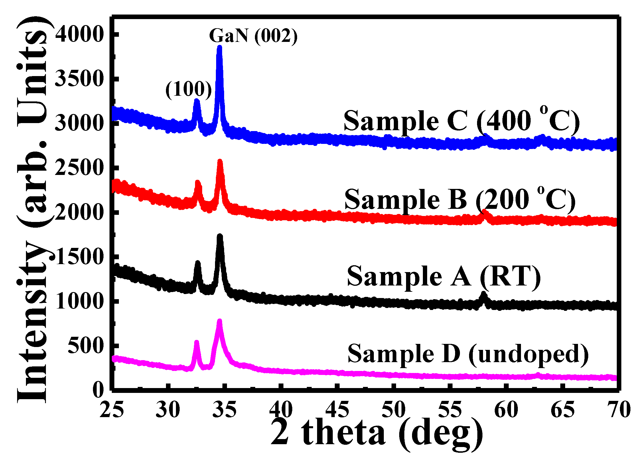
Figure 1 shows the X-ray diffraction (XRD) measurement results for Si-Ti-codoped GaN films of samples A, B, and C and the undoped GaN film of sample D. The XRD spectra show peaks at 2θ angles of 32.5° and 34.5°, corresponding to the (100) and (002) crystal orientations, respectively, of the GaN films. Moreover, the dominant peak at the (002) peak of GaN thin films indicated that the sputtering-deposited GaN thin films preferentially grow with a c-axis orientation and that the crystal quality of the GaN thin films was significantly improved by thermal annealing process.
Figure 1 shows that samples A, B, and C demonstrated that 2θ for the (002) crystal orientations was approximately 34.5°, similar with that of the undoped GaN film in sample D, indicating a slight distortion of the crystal lattice of GaN thin films after Si-Ti codoping [
18,
20]. Moreover, the XRD intensity of the (002) crystal orientation increased as the full width at half maximum (FWHM) decreased from 0.536° to 0.418°, with an increase in the annealing temperature from RT to 400 °C, indicating that the crystal quality improved with thermal annealing. Meanwhile, all the Si-Ti-codoped GaN films exhibited narrower FWHM values than that of the undoped GaN film in sample D, revealing the improved crystal quality by the Si-Ti-codoping technique and the thermal annealing process in this study.
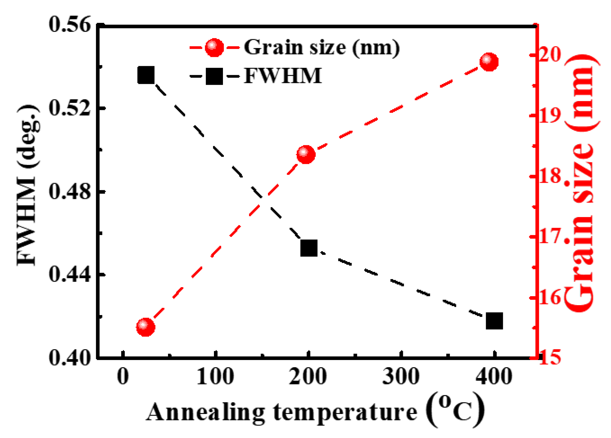
The grain sizes of the GaN films can be determined from the FWHMs of the XRD spectra using the Scherrer formula [
23]:
where D is the grain size, λ the X-ray wavelength of 0.154 nm, β the XRD (002) FWHM, and θ the Bragg angle. In
Figure 2, the calculated grain sizes and the corresponding XRD FWHM values of samples A, B, and C are displayed. The increased GaN crystallite size from 15.51 nm (sample A) to 19.89 nm (sample C) can be clearly observed, and this agrees with the AFM measurement results. At high annealing temperatures, the GaN surface adatoms possess increased thermal energy for enhanced surface diffusion, leading to the formation of more compact grains [
24]. The enlarged crystallite size with increased annealing temperature as calculated from the XRD results for the GaN samples should lead to a reduction in grain-boundary scattering in the GaN thin films and, in turn, to increased carrier mobility [
25].
The carriers are easily captured by the crystal defects in the GaN films forming the negative space charge. This causes electron scattering which subsequently results in a reduction in carrier mobility and carrier concentration. Therefore, the employment of an appropriate buffer layer between the GaN film and the glass substrate is extremely important. In this study, the ZnO buffer layer was adopted because high crystal quality of the ZnO layer was easily grown on the glass substrate with the sputtering-deposition method; meanwhile, there existed a low lattice mismatch of 2.2% between the ZnO and GaN layer, which could lead to the decrease in crystal defects in the GaN films. Therefore, the adoption of ZnO buffer layer could improve the crystal quality of the GaN films, and thus the enhanced carrier mobility in the Hall measurement.
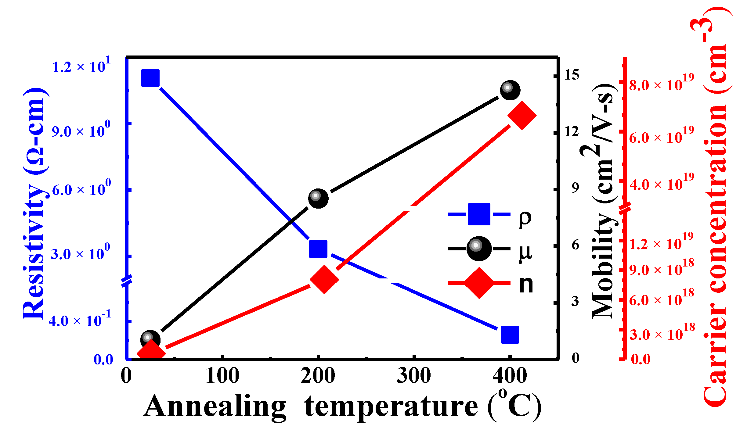
The electrical properties of the n-GaN thin-film samples A, B, C and un-doped GaN thin film (sample D) were determined by Hall measurements, and the results are shown in
Table 1 and
Figure 3. For the undoped GaN thin film of sample D, the electrical properties were observed with carrier concentration of 2.84 × 10
16 cm
−3, carrier mobility of 0.81 cm
2/V-s and thin-film resistivity of 648.83 ohm-cm. Compared with the sample D, the Si-Ti-codoped n-type GaN thin films in samples A show improved carrier concentration and carrier mobility. The low carrier mobility in sample D was ascribed to the scattering effects caused by considerable crystal defects and vacancies indicated by a larger FWHM value in the XRD results. In regard to incorporating the Si-Ti doping species in sputtering-deposited GaN films, the increased electron concentration was able to fill in the electron traps as well as the nonradiative recombination centers and, thus, it was screened from the defect scattering effects and contributed to the increased carrier mobility. According to the results of the Hall measurements, the electron concentration, thin-film resistivity, and carrier Hall mobility of sample A were 5.57 × 10
17 cm
−3, 11.06 Ω-cm, and 1.02 cm
2/V-s, respectively. The electrical properties of sample A indicate that the n-GaN film produced by our Si-Ti-co-doped sputtering technique exhibited improved carrier concentration and thin-film resistivity in comparison to the previously reported un-doped GaN thin films. The reduced thin-film resistivity was caused by the shallow ionization energy of 30 meV in the case of Si doping and by the shrinkage of the GaN energy band gap in the case of Ti doping [
14,
21]. In addition, after increasing the annealing temperature from RT to 400 °C (i.e., in the case of sample C), the electron concentration, thin-film resistivity, and carrier Hall mobility showed pronounced improvements of 6.65 × 10
19 cm
−3, 0.26 Ω-cm, and 14.25 cm
2/V-s, respectively. The Hall measurement results show that sample A, which was not subjected to the thermal annealing process, had a low carrier concentration; this was because the substitution of Ga atoms by Si and Ti atoms was less at the lower thermal energies. Moreover, the insufficient activation of dopants in the GaN thin film that was not subjected to thermal annealing could also result from the low degree of crystallization, thus causing low carrier concentration in sample A. However, the electrical properties of sample C show a significant improvement as a result of the thermal annealing process at the increased annealing temperature of 400 °C. The enhancement of the electron concentration from 5.57 × 10
17 to 6.65 × 10
19 cm
−3 in sample C can be attributed to the increased thermal activation of impurity dopants of group-IV elements (Si
4+ and Ti
4+) at this high annealing temperature, which allowed them to substitute for Ga
3+, thereby providing additional electrons in the n-GaN thin films [
26].
The low carrier mobility of sample A could furthermore result from the prominent boundary scattering in GaN samples with insufficient thermal energies that would result in high thin-film resistivity. However, the carrier mobility of the GaN thin film can be improved by increasing the annealing temperature. In this work, the annealing process was adopted to improve the carrier mobility from 1.02 cm
2/V-s (sample A) to 14.25 cm
2/V-s (sample C) because of the reduction in the carrier scattering effect associated with the reduced crystal defects of the GaN film with an elevated annealing temperature of 400 °C. In addition, the increased carrier concentration was also due to the reduced activation energy and reduced nonradiative recombination centers for an improved GaN crystal quality. Hence, the increase in carrier mobility and carrier concentration combined with the increased annealing temperature indicated the improvement of the crystalline quality [
27]. In addition, GaN thin-film crystallites were able to be more compact and denser in sample C due to the increased thermal energies at elevated annealing temperatures. An enlarged crystallite size of the GaN film in sample C with its high annealing temperature could also contribute to the reduction in grain-boundary scattering, resulting in the increased carrier mobility in sample C; this, in turn, would result in the electrical resistivity decreasing from 11.06 to 0.26 Ω-cm.
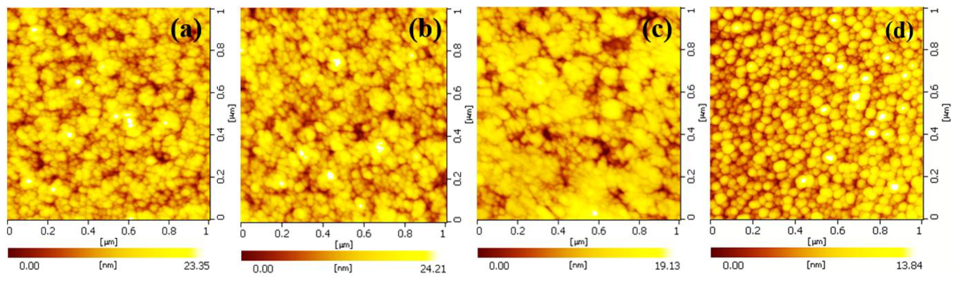
The surface morphology of the Si-Ti-codoped and undoped GaN films for samples A, B, C, and D was analyzed by atomic force microscopy (AFM) as shown in
Figure 4a–d, respectively. The grain sizes of the GaN films were measured as 13.89, 17.61, 18.13 nm, and 11.75 for the GaN thin films in samples A, B, C, and D, respectively. The small grain size of samples A and D (without any annealing) was due to insufficient thermal energy and subsequent low surface diffusion of adatoms for crystal growth; this results in small crystallite formation. The increase in grain size of the GaN thin films to 18.13 nm as the annealing temperature increased from RT to 400 °C was due to crystallite interaction and aggregation at high annealing temperatures. Moreover, the AFM measurement demonstrated that the film roughness decreased from 3.57 to 2.80 nm as the annealing temperature increased from RT to 400 °C, while the surface roughness was 4.12 nm for sample D. The tendency toward decreased surface roughness is attributable to the increased thermal energy and enhanced diffusion of surface atoms, which could lead to enhanced crystallite growth, resulting in enlarged grain size and dense, flat thin-film growth. Therefore, according to the AFM data, the GaN thin film in sample C demonstrated the largest grain size (18.13 nm) and the smallest roughness (2.80 nm).
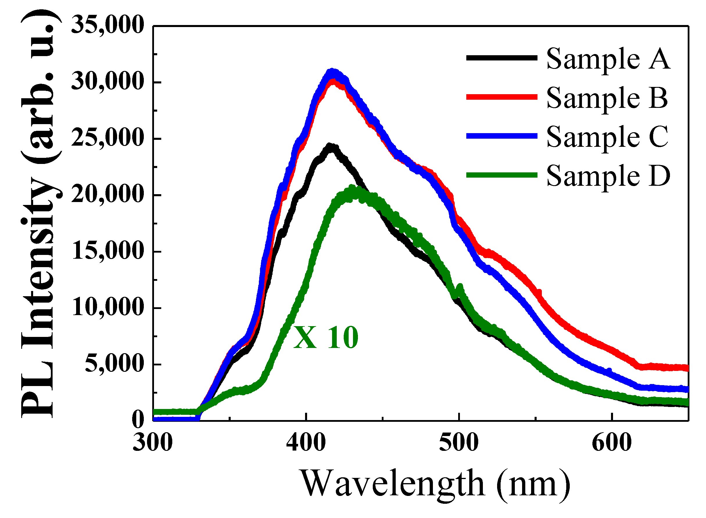
In
Figure 5, the results of RT photoluminescence (PL) measurements of samples A, B, C and D are presented. The optical properties, energy bandgap, and carrier energy transition behavior in n-type GaN thin films were analyzed in detail. As shown in
Figure 5, GaN films exhibit two dominant emission peaks at around 365 and 413 nm. The peak signal at 365 nm is related to the near-band-edge (NBE) emission for the carrier transition from the valence band to the lowest allowed energy states in the conduction band of the GaN thin film with a hexagonal crystal structure [
28]. The typical blue luminescence (BL) band in GaN thin films was observed at the peak position in the range from 3.0 to 2.7 eV, and the dominant BL peak in this study was at 3.0 eV (413 nm). The PL emission peak at 413 nm can be ascribed to the energy transition from the conduction band or a shallow donor level to a deep acceptor level. Density functional theory calculations demonstrated the carrier transition from the C
Ga donor level to the C
N acceptor level because the carbon impurities in the GaN films can account for the BL band at the PL peak signal of approximately 413 nm (3.0 eV) [
29,
30]. The considerable Carbon (C) impurity may be attributable to the fact that the sputtering system employed here belongs to a public instrument; therefore, a variety of material systems are fabricated in the same chamber (e.g., Silicon Carbide (SiC) and other C-containing materials). Therefore, in this study, the GaN films demonstrated C contamination, resulting in a substantial amount of unexpected impurities in them. As shown in
Figure 5, the intensity of the NBE emission peak signal was enhanced by performing a thermal annealing process that elevated the temperature from RT to 400 °C; this indicates that enhanced crystallization increased the GaN grain size, thereby improving the GaN crystal quality. In addition,
Figure 5 demonstrates that the intensity of the peak signal at 413 nm (3.0 eV) depended on the annealing temperature. This could be related to enhanced Ga atom substitution by C impurities at high annealing temperatures, leading to an increased number of carrier transitions from the C
Ga donor level to the C
N acceptor level as the annealing temperature increased.
Additionally, the PL intensity of the NBE emission for the Si-Ti-codoped GaN films were significantly increased compared with that of the undoped GaN film in sample D, indicating the improved crystal quality by the Si-Ti-codoping technique in samples A, B and C. The improved crystal quality by the PL measurement was also agreed well with the study results of the XRD measurement in
Figure 1.
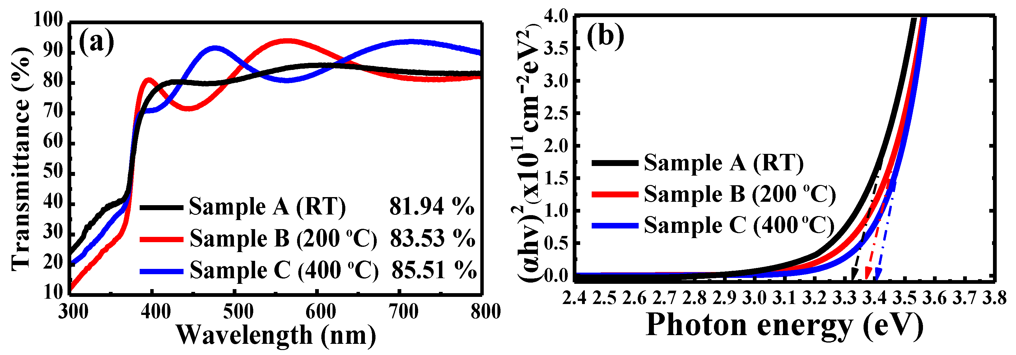
Figure 6 shows the transmittance of GaN thin-film samples A, B, and C in the range of 300 to 800 nm. The average transmittances of the Si-Ti-codoped GaN film were 81.94, 83.53, and 85.51% at annealing temperatures of RT, 200 °C, and 400 °C, respectively. As shown in
Figure 6a, the absorption edge for all GaN samples occurs at approximately 365 nm. Since the GaN thin films deposited by the sputtering system exhibited the polycrystalline structure, the grain-boundary scattering could be the dominant effects responsible for the transmittance. The grain size of the GaN film was found to be increased when increasing the annealing temperatures from RT to 400 °C, as evident in the AFM and XRD studies. Hence, the reduction in the optical scattering by the reduced grain boundaries could contribute to the increase in the optical transmittance in the dense GaN films with enlarged grain size [
31]. Additionally, through the AFM measurement, it can be observed that sample C exhibit the reduced surface roughness compared with the other GaN samples, which could also lead to the increased transmittance due to the reduced surface scattering [
32]. To investigate the relationship between the optical and the electronic properties of the GaN thin films, a Tauc plot was calculated using Equation (2) and the data from the transmittance measurement:
where α is the absorption coefficient, h Planck’s constant, ν the photon frequency, A a proportionality constant, and E
g the energy bandgap of the material. Furthermore, n = 1/2 was adopted here because of the direct transitions of GaN films. As displayed in
Figure 6b, the optical bandgap values of the GaN films exhibited an increasing trend from 3.33 to 3.41 eV for samples A to C as the annealing temperatures increased from RT to 400 °C. In addition, the transmittance edge shifted to higher bandgap from 3.33 to 3.41 nm for samples A to C; this might be due to the Burstein–Moss effect. The Burstein–Moss effect resulted from the high doping concentration which will cause the blue shift of the optical absorption edge. As the distribution of the degenerated semiconductor’s electron is full at the near-band edge of the conduction band, it causes the higher transition energy from the valence band. Hence, the tendency of the enlarge bandgap or the blue shift of the optical absorption edge was named the Burstein–Moss shift [
33,
34]. According to Lee’s report, they found that the photoluminescence peak signal position of the highly compensated Si-doped GaN film decreased as the electron concentration increased, which was due to the forbidden band-edge fluctuation resulting from residual impurities [
35]. Moreover, the band gap renormalization was similar to the band gap narrowing effect. These can be explained by the decrease in the bandgap as the doping concentration rises due to its self-energy effect [
36]. Notably, the Fermi level inside the conduction band moves upward, indicating an increased carrier concentration of the GaN films with an annealing temperatures ranging from RT to 400 °C [
37]. This trend in the Tauc plot results agrees with the effects of an increased electron concentration in the Hall measurement.
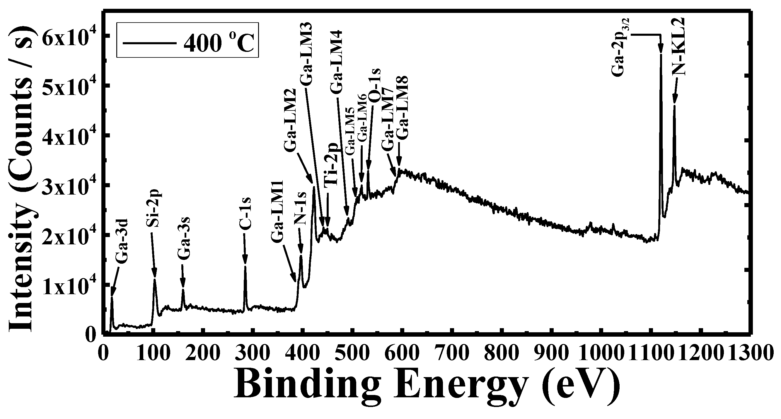
The chemical composition of the Si-Ti-codoped GaN film annealed at 400 °C was analyzed by X-ray photoelectron spectroscopy (XPS), as shown in
Figure 7. The binding energies of Gallium on the 3d orbital (Ga-3d), Silicon on the 2p orbital (Si-2p), Nitrogen on the 1s orbital (N-1s), Titanium on the 2p orbital (Ti-2p), and Gallium on the 2p
2/3 orbital (Ga-2p
3/2) were 19.7, 102.6, 397.3, 455.6, and 1119.5 eV, respectively. The C-1s spectrum was calibrated at 284.6 eV as a reference element for all signals. The high-resolution Ga-3d XPS spectra with fitting curves showed that the Ga-3d spectrum consisted of the Ga–Ga bond, the Ga–N bond, and the Ga–O bond; the binding energies of these were 18.2, 19.7, and 20.5 eV, respectively, as shown in
Figure 8a. These binding energy values are in agreement with other reported results [
38]. The Si-2p spectrum with fitting curves shown in
Figure 8b was composed of the Si–Si bond, the Si–N bond [
39], and the Ga–N bond [
40] with corresponding binding energies of 99.1, 102.6, and 106.1 eV. The appearance of the Ga–N bond in the Si-2p spectrum can be ascribed to the similarity in the binding energy values between Si-2p and Ga-3p
1/2. The N-1s spectrum shown in
Figure 8c is made up of two peaks corresponding to the binding energies of 392.7 and 397.3 eV, respectively. The binding energy at 392.7 eV can be attributed to the Ga LMM Auger transitions that revealed the presence of metallic-like Ga [
41]. The peak at 397.3 eV appearing in the N-1s spectrum corresponds to the bonding between gallium and nitrogen atoms, thus forming the Ga–N bond. In addition, it can be seen in
Figure 8d that Ga-2p
3/2 has a dominant peak at 1118.7 eV and a smaller peak at 1119.5 eV.
The binding energy at 1118.7 eV could be ascribed to the bonding between the Ga–N components while the binding energy at 1119.5 eV corresponds to the Ga–O bond [
42,
43]. According to Dasari’s report, the binding energy standard of the Ga-2p
3/2 was 1117 eV, which is lower than our result, and it can be ascribed to the formation of a nitride compound. This result of Ga-2p
2/3 agrees with the result of Ga-3d, which appears to have a greater amount of the Ga-N bond than the Ga-O bond [
44]. As shown in
Figure 8e, the XPS peak belonging to Ti-2p was analyzed based on the XPS spectral survey scan, and the binding energy of both Ti-O, and Ti-N was 458.8, 464.6 eV and 461.0 eV, respectively [
45,
46]. The high XPS intensity in Ti-O bonding might be due to the Ti bonding with the oxide residue during the sputtering-deposition of ZnO buffer layer. The high XPS intensity of the Ga–O bond in the GaN thin film might be due to the unintentional oxygen adsorption of the GaN thin-film surface and the residual oxide compound in the growth chamber after the sputtering deposition of the ZnO buffer layer. The XPS measurement results indicate that all atoms doped into the GaN film are present and that both Si and Ti bond with N atoms.


