A Comparative Study of Theoretical Methods to Estimate Semiconductor Nanoparticles’ Size

 ,
,  and
and
Abstract
1. Introduction
2. Materials and Methods
2.1. Materials
2.2. Characterization
2.3. Models
2.3.1. Brus Model
2.3.2. Hyperbolic Band Model (HBM)
2.3.3. Empirical Formula Suggested by Henglein et al.
2.3.4. Empirical Formula Obtained by Yu et al.
2.4. Synthesis of CdS Nanocrystals
3. Results
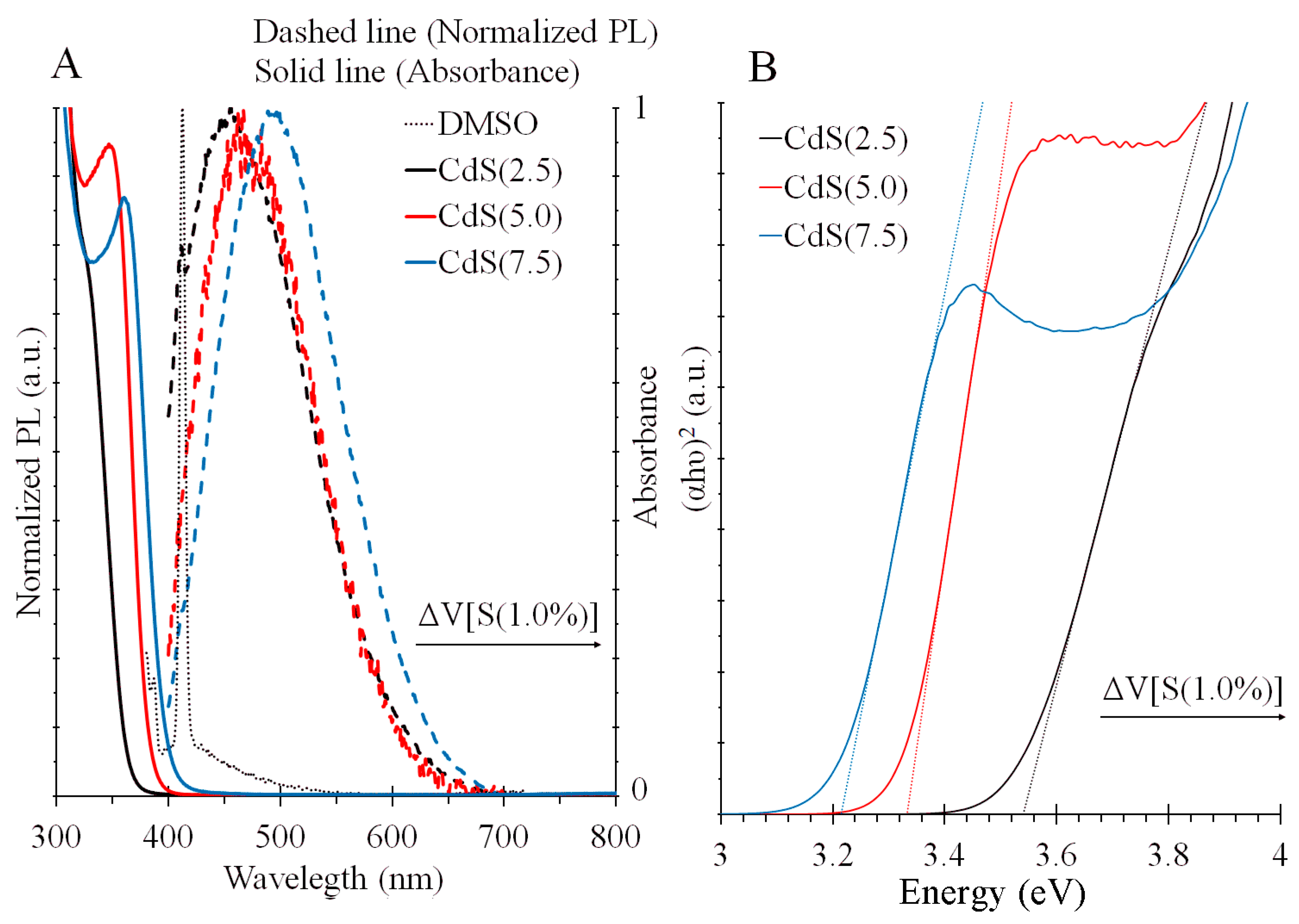
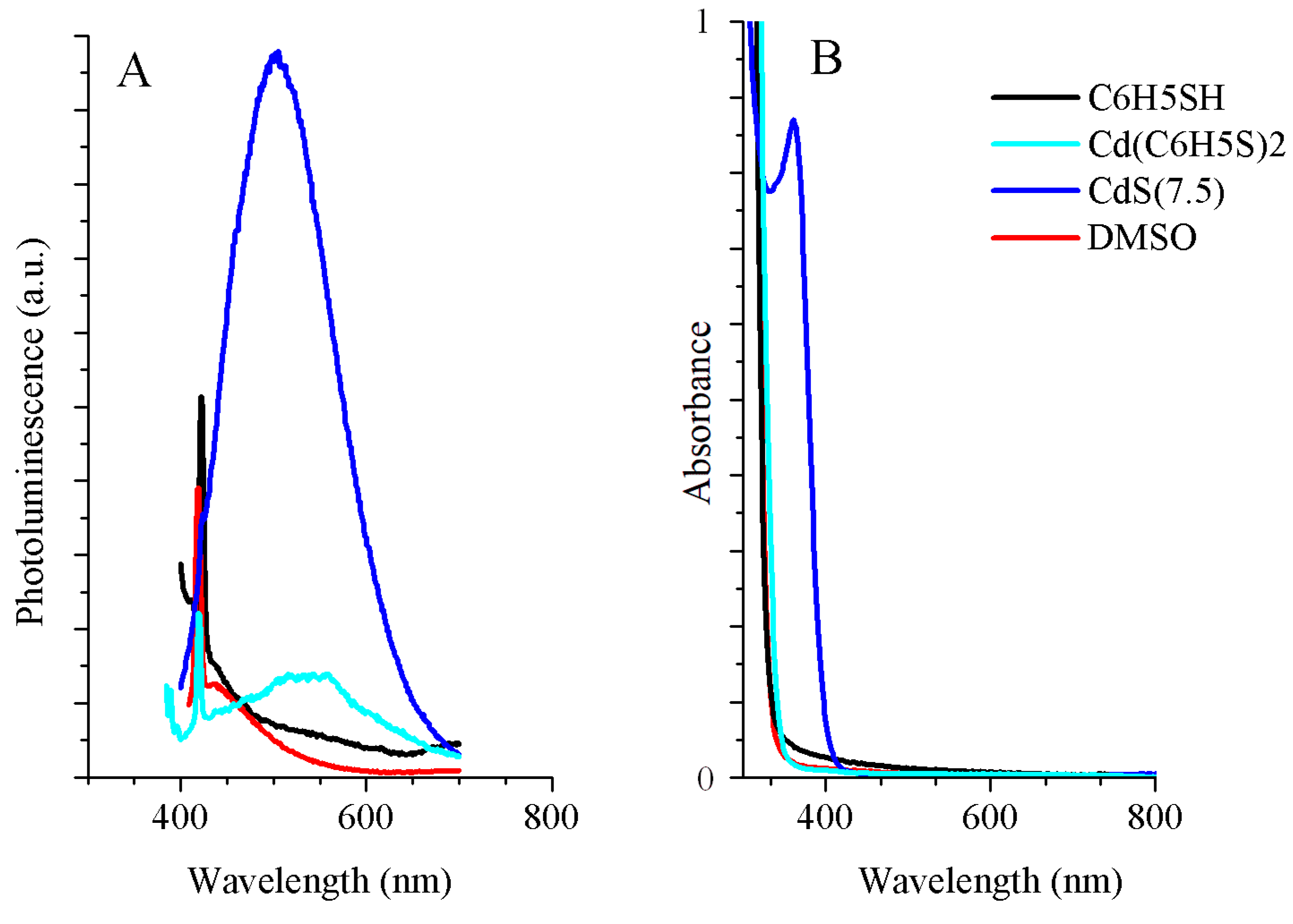
3.1. Optical Characterization
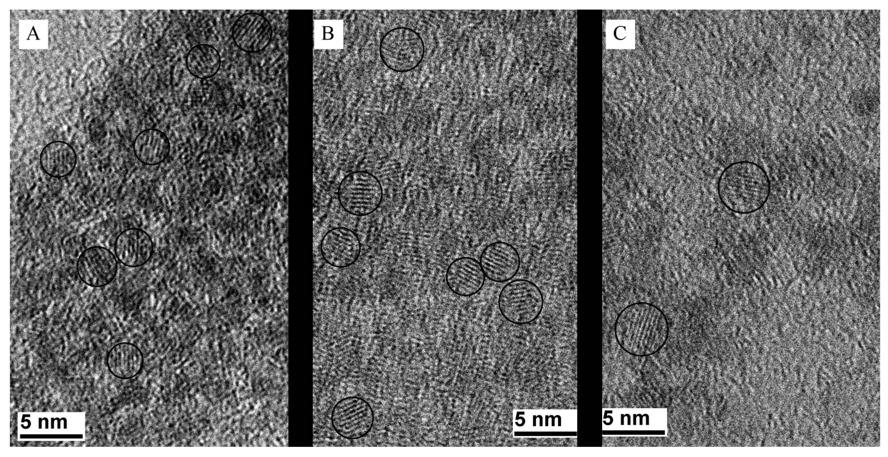
3.2. TEM Study
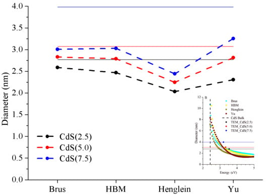
3.3. Comparison of Theoretical Models to Estimate CdS Size
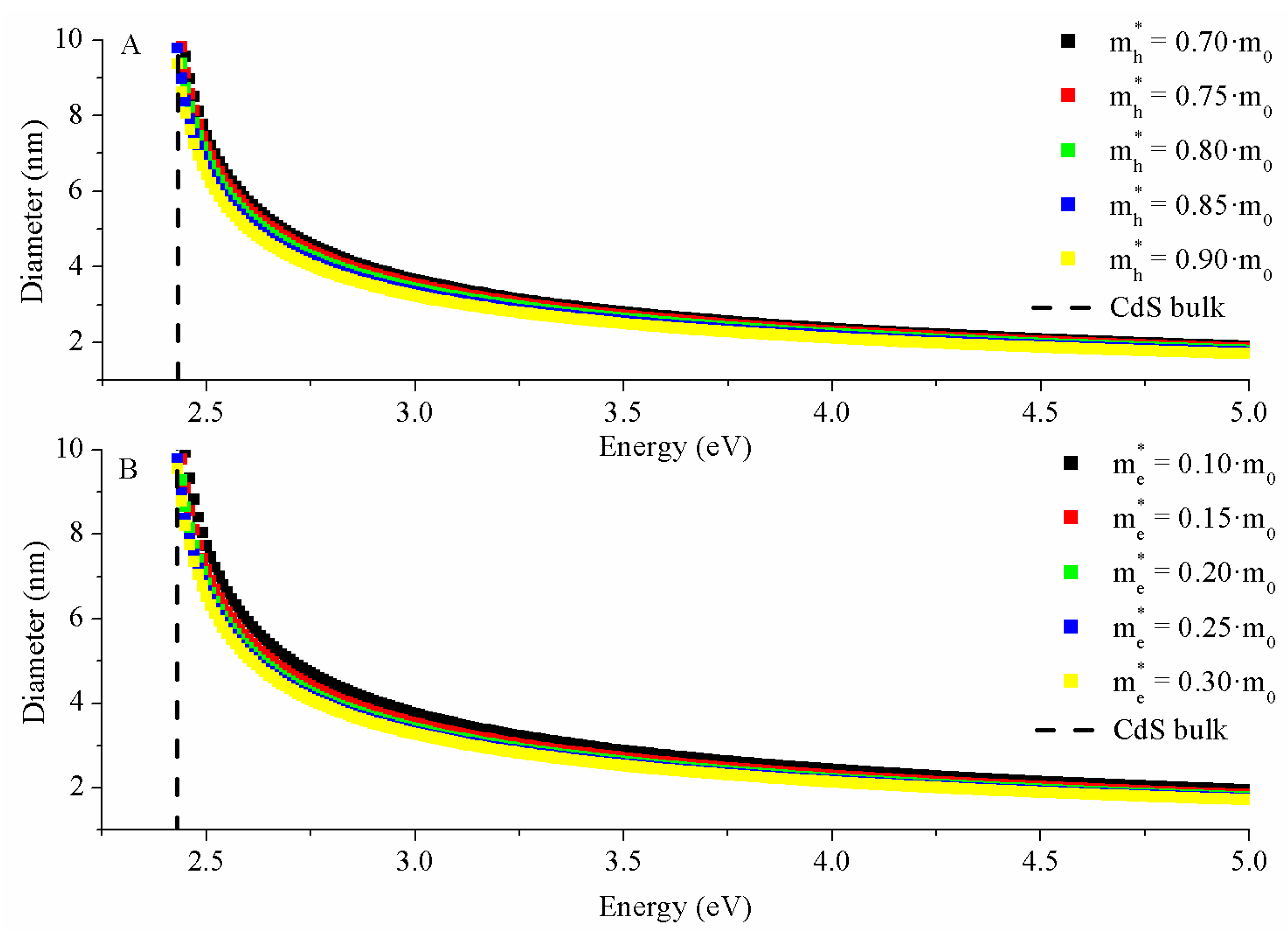
3.3.1. Brus Model
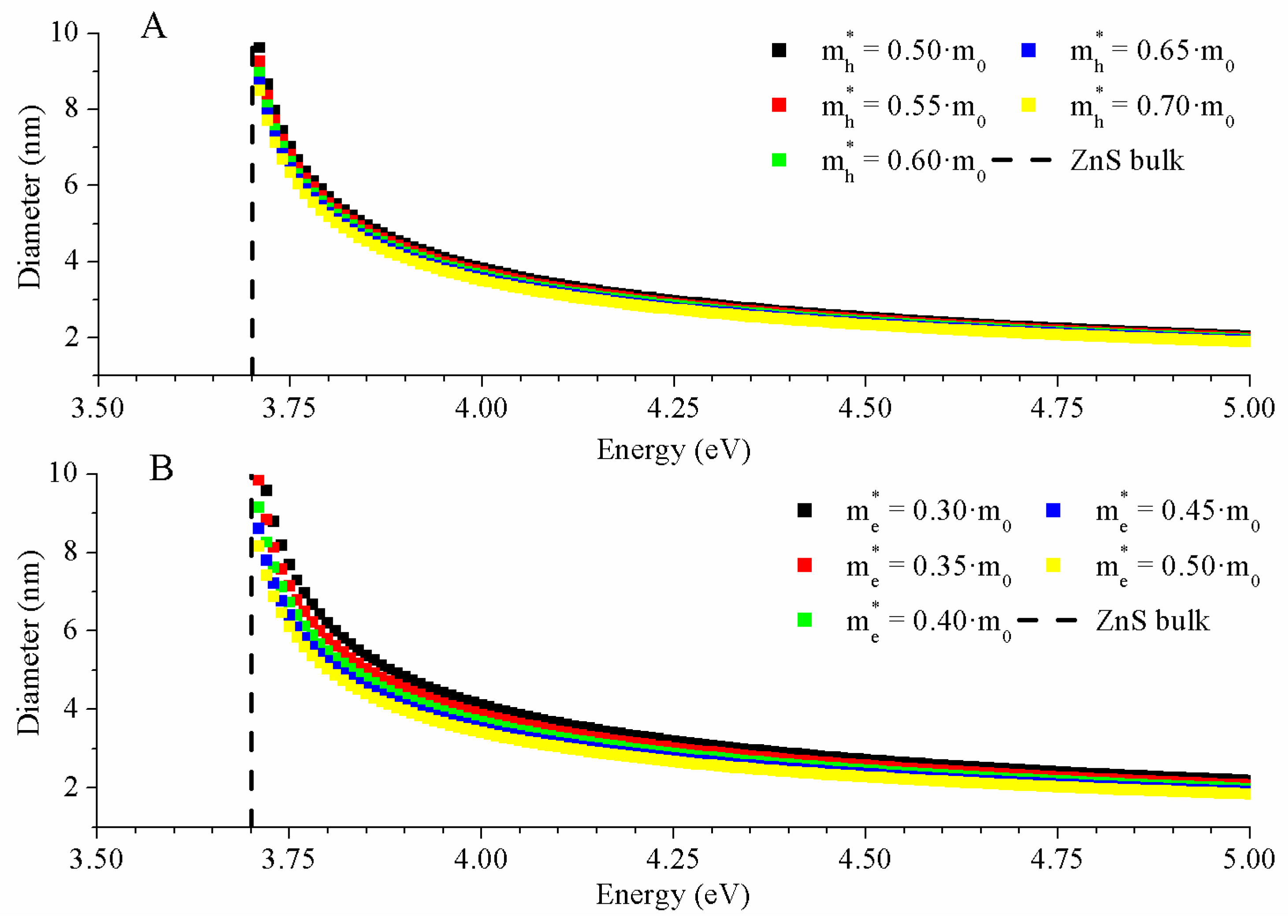
3.3.2. HBM Model
3.3.3. Henglein Model and Yu Equation
4. Conclusions
Author Contributions
Funding
Conflicts of Interest
References
- Kiyohara, S.; Fujiwara, M.; Matsubayashi, F.; Mori, K. Organic light-emitting microdevices fabricated by nanoimprinting technology using diamond molds. Jpn. J. Appl. Phys. 2005, 44, 3686–3690. [Google Scholar] [CrossRef]
- Pu, Y.; Chen, Y. Solution-processable bipolar hosts based on triphenylamine and oxadiazole derivatives: Synthesis and application in phosphorescent light-emitting diodes. J. Lumin. 2016, 170, 127–135. [Google Scholar] [CrossRef]
- Alonso, J.L.; Ferrer, J.C.; Rodríguez-Mas, F.; Fernández de Ávila, S. Improved P3HT:PCBM photovoltaic cells with two-fold stabilized PbS nanoparticles. Optoelectron. Adv. Mat. 2016, 10, 634–639. [Google Scholar]
- Pugazhendhi, A.; Edison, T.N.J.I.; Karuppusamy, I.; Kathivel, B. Inorganic nanoparticles: A potential cancer therapy for human welfare. Int. J. Pharm. 2018, 539, 104–111. [Google Scholar] [CrossRef]
- Pavel, F.M.; Mackay, R.A. Reverse micellar synthesis of a nanoparticle/polymer composite. Langmuir 2000, 16, 8568–8574. [Google Scholar] [CrossRef]
- Feldheim, D.L.; Keating, C.D. Self-assembly of single electron transistors and related devices. Chem. Soc. Rev. 1998, 27, 1–12. [Google Scholar] [CrossRef]
- Granot, E.; Patolsky, F.; Willner, I. Electrochemical assembly of a CdS semiconductor nanoparticle monolayer on surfaces: Structural properties and photoelectrochemical applications. J. Phys. Chem. B 2004, 108, 5875–5881. [Google Scholar] [CrossRef]
- Cordoncillo, E.; Escribano, P.; Monrós, G.; Tena, M.A.; Orera, V.M.; Carda, J. The preparation of CdS particles in silica glasses by a sol-gel method. J. Solid State Chem. 1995, 118, 1–5. [Google Scholar] [CrossRef]
- Ferrer, J.C.; Salinas-Castillo, A.; Alonso, J.L.; Fernández de Ávila, S.; Mallavia, R. Direct synthesis of PbS nanocrystals capped with 4-fluorothiophenol in semiconducting polymer. Mater. Chem. Phys. 2010, 122, 459–462. [Google Scholar] [CrossRef]
- Schmitt, S.; Arditty, S.; Leal-Calderon, F. Stability of concentrated emulsions. Interface Sci. Technol. 2004, 4, 607–639. [Google Scholar] [CrossRef]
- Tauc, J.; Menth, A. State in the gap. J. Non-Cryst. Solids 1972, 8–10, 569–585. [Google Scholar] [CrossRef]
- Osuwa, J.C.; Oriaku, C.I.; Kalu, I.A. Variation of optical band gap with post deposition annealing in CdS/PVA thin films. Chalcogenide Lett. 2009, 6, 433–436. [Google Scholar]
- Brus, L. Electronic wave functions in semiconductor clusters: Experiment and theory. J. Phys. Chem. 1986, 90, 2555–2560. [Google Scholar] [CrossRef]
- Das, R.; Pandey, S. Comparison of optical properties of bulk and nano crystalline thin films of CdS using different precursors. Int. J. Mater. Sci. 2011, 1, 35–40. [Google Scholar]
- Moffitt, M.; Eisenber, A. Size Control of nanoparticles in Semiconductor-Polymer Composites. 1. Control via Multiplet Aggregation Numbers in Styrene-Based Random Ionomers. Chem. Mater. 1995, 7, 1178–1184. [Google Scholar] [CrossRef]
- Yu, W.W.; Qu, L.H.; Guo, W.Z.; Peng, X.G. Experimental Determination of the Extinction Coefficient of CdTe, CdSe, and CdS Nanocrystals. Chem. Mater. 2003, 15, 2854–2860. [Google Scholar] [CrossRef]
- Reimer, L.; Kohl, H. Transmission Electron Microscopy. Physics of Image Formation, 5th ed.; Elsevier: Heidelberg, Germany, 2008; ISBN 978-1-4419-2308-0. [Google Scholar]
- Rodríguez-Mas, F.; Fernández de Ávila, S.; Ferrer, J.C.; Alonso, J.L. Expanded Electroluminescence in High Load CdS Nanocrystals PVK-Based LEDs. Nanomaterials 2019, 9, 1212. [Google Scholar] [CrossRef]
- Hullavard, N.V.; Hullavard, S.S.; Karulkar, P.C. Cadmium sulphide (CdS) nanotechnology: Synthesis and applications. J. Nanosci. Nanotechnol. 2008, 8, 3272–3299. [Google Scholar] [CrossRef]
- Zhou, A.P.; Sheng, W.D. Electron and hole effective masses in self-assembled quantum dots. Eur. Phys. J. B. 2009, 68, 233–236. [Google Scholar] [CrossRef]
- Tan, S.G.; Jalil, M.B.A. 2—Nanoscale physics and electronics. In Introduction to the Physics of Nanoelectronics, 1st ed.; Woodhead Publishing Limited: Cambridge, UK, 2012; pp. 23–77. [Google Scholar] [CrossRef]
- Unni, C.; Philip, D.; Smitha, S.L.; Nissamudeen, K.M.; Gopchandran, K.G. Aqueous synthesis and characterization of CdS, CdS:Zn2+ and CdS:Cu2+ quantum dots. Spectrochim. Acta A Mol. Biomol. Spectrosc. 2009, 72, 827–832. [Google Scholar] [CrossRef]
- Praus, P.; Svoboda, L.; Horínková, P. Preparation and optical absorption of CdS, ZnS, ZnXCd1-XS and core/shell CdS/ZnS nanoparticles. Nanocon 2013, 10, 16–18. [Google Scholar]
- Dey, P.C.; Das, R. Photoluminescence quenching in ligand free CdS nanocrystals due to silver doping along with two high energy surface states emission. J. Lumin. 2017, 183, 368–376. [Google Scholar] [CrossRef]
- Henglein, A. Small-particle research: Physicochemical properties of extremely small colloidal metal and semiconductor particles. Chem. Rev. 1989, 89, 1861–1873. [Google Scholar] [CrossRef]
- Wang, Y.; Suna, A.; Mahler, W.; Kasowski, R. PbS in polymers. From molecules to bulk solids. J. Chem. Phys. 1987, 87, 7315–7322. [Google Scholar] [CrossRef]
- Nanda, K.K.; Kruis, F.E.; Fissan, H.; Behera, S.N. Effective mass approximation for two extreme semiconductors: Band Gap of PbS and CuBr nanoparticles. J. Appl. Phys. 2004, 95, 5035. [Google Scholar] [CrossRef]
- Spanhel, L.; Haase, M.; Weller, H.; Henglein, A. Photochemistry of colloidal semiconductors. 20. Surface modification and stability of strong luminescing CdS particles. J. Am. Chem. Soc. 1987, 109, 5649–5655. [Google Scholar] [CrossRef]
- Boles, M.A.; Ling, D.; Hyeon, T.; Talapin, D.V. The surface science of nanocrystals. Nat. Mater. 2016, 15, 141–153. [Google Scholar] [CrossRef]
- Ferrer, J.C.; Salinas-Castillo, A.; Alonso, J.L.; Fernández de Ávila, S.; Mallavia, R. Influence of SPP co-stabilizer on the optical properties of CdS quantum dots grown in PVA. Phys. Procedia 2009, 2, 335–338. [Google Scholar] [CrossRef][Green Version]
- Heiba, Z.K.; Mohamed, M.B.; Imam, N.G. Fine-tune optical absorption and light emitting behavior of the CdS/PVA hybridized film nanocomposite. J. Mol. Struct. 2017, 1136, 321–329. [Google Scholar] [CrossRef]
- Ning, Z.; Molnár, M.; Chen, Y.; Friberg, P.; Gan, L.; Ågren, H.; Fu, Y. Role of surface ligands in optical properties of colloidal CdSe/CdS quantum dots. Phys. Chem. Chem. Phys. 2011, 13, 5848–5854. [Google Scholar] [CrossRef]
- Brus, L. Electron-electron and electron-hole interactions in small semiconductor crystallites: The size dependence of the lowest excited electronic state. J. Chem. Phys. 1984, 80, 4403–4409. [Google Scholar] [CrossRef]
- Souci, A.H.; Keghouche, N.; Delaire, J.A.; Remita, H.; Etcheberry, A.; Mostafavi, M. Structural and Optical Properties of PbS Nanoparticles Synthesized by the Radiolytic Method. J. Phys. Chem. C 2009, 113, 8050–8057. [Google Scholar] [CrossRef]


| NPs | m[Cd(C6H5-SH)] | V[DMSO] | V[S(1%)] |
|---|---|---|---|
| CdS(2.5) | 0.80 g | 20 mL | 2 mL |
| CdS(5.0) | 0.80 g | 20 mL | 4 mL |
| CdS(7.5) | 0.80 g | 20 mL | 6 mL |
| NPs | Absorption Edge | PL Peak | |
|---|---|---|---|
| CdS(2.5) | 3.54 eV | 350 nm | 456 nm |
| CdS(5.0) | 3.33 eV | 372 nm | 480 nm |
| CdS(7.5) | 3.21 eV | 386 nm | 495 nm |
| NPs | Brus | HBM | Henglein | Yu |
|---|---|---|---|---|
| CdS(2.5) | −6% | −11% | −30% | −25% |
| CdS(5.0) | −8% | −9% | −30% | −16% |
| CdS(7.5) | −24% | −24% | −42% | −26% |
© 2020 by the authors. Licensee MDPI, Basel, Switzerland. This article is an open access article distributed under the terms and conditions of the Creative Commons Attribution (CC BY) license (http://creativecommons.org/licenses/by/4.0/).
Share and Cite
Rodríguez-Mas, F.; Ferrer, J.C.; Alonso, J.L.; Valiente, D.; Fernández de Ávila, S. A Comparative Study of Theoretical Methods to Estimate Semiconductor Nanoparticles’ Size. Crystals 2020, 10, 226. https://doi.org/10.3390/cryst10030226
Rodríguez-Mas F, Ferrer JC, Alonso JL, Valiente D, Fernández de Ávila S. A Comparative Study of Theoretical Methods to Estimate Semiconductor Nanoparticles’ Size. Crystals. 2020; 10(3):226. https://doi.org/10.3390/cryst10030226
Chicago/Turabian StyleRodríguez-Mas, Fernando, Juan Carlos Ferrer, José Luis Alonso, David Valiente, and Susana Fernández de Ávila. 2020. "A Comparative Study of Theoretical Methods to Estimate Semiconductor Nanoparticles’ Size" Crystals 10, no. 3: 226. https://doi.org/10.3390/cryst10030226
APA StyleRodríguez-Mas, F., Ferrer, J. C., Alonso, J. L., Valiente, D., & Fernández de Ávila, S. (2020). A Comparative Study of Theoretical Methods to Estimate Semiconductor Nanoparticles’ Size. Crystals, 10(3), 226. https://doi.org/10.3390/cryst10030226