Article

Depth Profiling of Ion-Implanted 4H–SiC Using Confocal Raman Spectroscopy

1
State Key Laboratory of Precision Measuring Technology & Instruments, Centre of Micro/Nano Manufacturing Technology, Tianjin University, Tianjin 300072, China
2
Fraunhofer Institute for Integrated Systems and Device Technology, Schottkystrasse 10, 91058 Erlangen, Germany
3
State Key Laboratory of Separation Membranes and Membrane Processes, School of Materials Science and Engineering, Tianjin Polytechnic University, Tianjin 300387, China
4
Department of Physics, Nankai University, Tianjin 300071, China
*
Authors to whom correspondence should be addressed.
Crystals 2020, 10(2), 131; https://doi.org/10.3390/cryst10020131
Submission received: 20 January 2020 / Revised: 13 February 2020 / Accepted: 19 February 2020 / Published: 21 February 2020

Abstract

:
For silicon carbide (SiC) processed by ion-implantation, dedicated test structure fabrication or destructive sample processing on test wafers are usually required to obtain depth profiles of electrical characteristics such as carrier concentration. In this study, a rapid and non-destructive approach for depth profiling is presented that uses confocal Raman microscopy. As an example, a 4H–SiC substrate with an epitaxial layer of several micrometers thick and top layer in nanoscale that was modified by ion-implantation was characterized. From the Raman depth profiling, longitudinal optical (LO) mode from the epitaxial layer and longitudinal optical phonon-plasmon coupled (LOPC) mode from the substrate layer can be sensitively distinguished at the interface. The position profile of the LOPC peak intensity in the depth direction was found to be effective in estimating the thickness of the epitaxial layer. For three kinds of epitaxial layer with thicknesses of 5.3 μm, 6 μm, and 7.5 μm, the average deviations of the Raman depth analysis were −1.7 μm, −1.2 μm, and −1.4 μm, respectively. Moreover, when moving the focal plane from the heavily doped sample (~1018 cm−3) to the epitaxial layer (~1016 cm−3), the LOPC peak showed a blue shift. The twice travel of the photon (excitation and collection) through the ion-implanted layer with doping concentrations higher than 1 × 1018 cm−3 led to a difference in the LOPC peak position for samples with the same epitaxial layer and substrate layer. Furthermore, the influences of the setup in terms of pinhole size and numerical aperture of objective lens on the depth profiling results were studied. Different from other research on Raman depth profiling, the 50× long working distance objective lens (50L× lens) was found more suitable than the 100× lens for the depth analysis 4H–SiC with a multi-layer structure.

1. Introduction

As a third generation semiconductor material, silicon carbide has many outstanding characteristics such as a wide forbidden bandgap, high thermal conductivity, high mobility, and high electrical breakdown strength [1]. Ion-implantation is generally accepted to be the only feasible method for selective doping in light of the low diffusion coefficient of impurities in silicon carbide [2]. Ion-implantation was followed by a high temperature annealing treatment to achieve the electrical activation of dopant impurities and recovery of defects. It is worth noting that the implanted regions typically have thicknesses in the sub-micrometer range. To evaluate the electrical properties of the material obtained after ion-implantation and annealing treatment, where the carrier concentration and carrier mobility are of particular interest, and many methods are being used to measure the electrical properties of silicon carbide such as the Hall effect [3], point contact current voltage technique (PCIV) [4], four-point probe [5], and mercury-probe capacitance voltage [6]. Currently, most characterization methods for the electrical properties above-mentioned need the preparation of special measurement structures or will destroy the sample in the process of obtaining the depth distribution of electrical parameters, while the operation procedures are laborious and time consuming: (a) the point contact current voltage (PCIV) [7] has several drawbacks including rather low sensitivity and the lack of required reference samples; (b) the electrochemical etching based depth profiling [8] was investigated but also exhibited insufficient accuracy and reliability. For doping profiles with lower maximum doping concentrations (<~5 × 1017 cm−3 or even lower), the standard in industrial process control is based on well-established mercury capacitance voltage measurements, whereas basically similar but contactless methods seem to have arisen [9]. In addition, other techniques have been investigated and developed such as scanning spreading resistance microscopy (SSRM) or scanning capacitance microscopy (SCM), which, however, are time consuming and need elaborate sample preparation. For SCM, higher doping concentrations might be problematic as indicated in earlier works for 6H–SiC and also need appropriate calibration samples [10]. The most relevant method for rather thin implanted 4H–SiC layers with high doping concentrations is secondary ion mass spectroscopy (SIMS) depth profiling. However, this gives only the “chemical” depth profile of the implanted species [11]. Unfortunately, though, especially in 4H–SiC (compared to e.g., Si), the electrically active doping concentration and, thus, the carrier concentration profile might differ significantly from the chemically implanted concentrations. This is much more pronounced for Al-implantation than for N-implantation. All according methods have not asserted themselves yet due to the above given reasons. Therefore, it is very important to find alternative and non-destructive methods to evaluate the electrical properties profiling of ion-implanted silicon carbide.
Raman spectroscopy is a contactless optical detection method with good sensitivity and high detection efficiency. The confocal configuration formed by placing a micrometer sized pinhole in the back focal plane can greatly improve the spatial resolution of the obtained Raman spectrum and realize optical sectioning [12]. So far, only a small number of confocal depth analysis results have been published, but most of them have focused on the damage distribution after high energy (MeV range) implantation, which is not the typical case for silicon carbide doping in the SiC electrical device industry. Confocal Raman set-up was used to analyze the depth distribution of damage after high energy ion-implantation on the order of MeV before and after annealing treatment [13] and the information of the absorption coefficient could be extracted from a high dose Al-implanted layer in 6H–SiC [2,14]. Zuk destructively pretreated the sample and obtained the damage distribution of high-energy ion-implanted 6H–SiC by confocal Raman spectroscopy on the processed slope, which requires rigorous and complex sample pretreatment and the sample cannot be re-used or further processed after the test [15]. De Biasio demonstrated the use of Raman spectroscopy for the determination of carrier concentrations in epitaxial layers and substrates in n-type 4H–SiC obtained by doping during epitaxial growth without a detailed explanation of the overlap of the longitudinal optical (LO) mode and the longitudinal optical phonon-plasmon coupled (LOPC) mode [16]. Tao Liu et al. studied the phenomenon of photo-generated carriers excited by ultraviolet light (325 nm line) and calculated the carrier concentrations of the epitaxial layer [17]. However, the research did not focus on the epitaxial layer thickness, the variation of the LOPC peak position in the depth direction, and the influence of different doping concentrations on the position of the LOPC peak. Aside from this, there has been no integrated report on the depth profiling of p-type ion-implanted 4H–SiC by confocal Raman microscopy, which typically has multilayer structures along the depth direction.
In this study, confocal Raman spectroscopy was used to analyze the depth profiling of 4H–SiC processed by ion-implantation and annealing treatments for p-type ion-implanted 4H–SiC. Information on the heavily doped substrate and epitaxial layer were distinguished, the thickness of the epitaxial layer was evaluated, and the influence of the top ion modified layer on the Raman depth analysis was explained in detail.

2. Experimental Setups

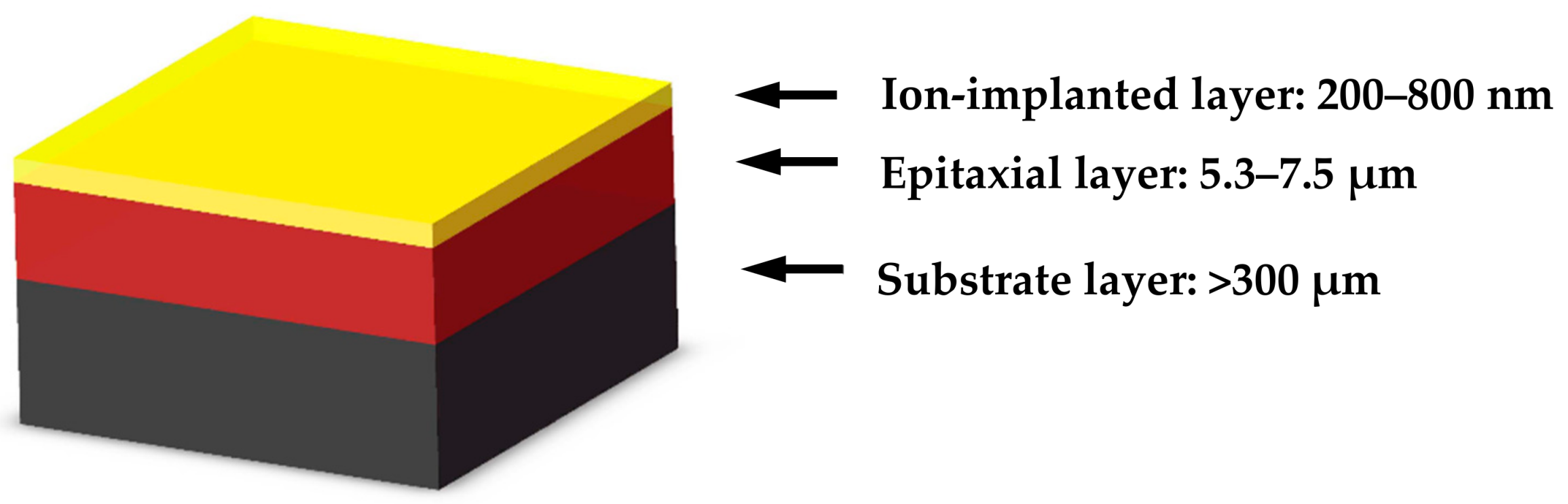
2.1. Sample Description

The starting materials were 4H–SiC (0001) nitrogen doped (N-doped) n+ substrates obtained from Dow Corning and SiCrystal (Germany). N-doped epitaxial layers of 5.3 μm, 6 μm and 7.5 μm were grown on substrates with 4° ± 0.5° off-axis toward <11–20> by the chemical vapor deposition (CVD) process. Multiple aluminum ion-implantations were used to achieve the uniform p-type doping profile. The implantation depth varied between 200 and 800 nm (criterion: NA = ND) [18]. Then, the samples were annealed at different temperatures of 1700 °C, 1800 °C, and 1900 °C with a capping layer. The samples had a multilayer structure, as shown in Figure 1, which includes heavily doped n-type substrates of several hundred microns, n-type epitaxial layers of several microns, and p-type ion-implanted layers of several hundred nanometers (except for the un-implanted sample G and the substrate material). Details of the sample preparation parameters are shown in Table 1.

2.2. Measurement Setups

The Raman measurements were performed at room temperature in backscattering geometry using a Horiba XploRA PLUS (Minami-ku, Kyoto, Japan) equipped with a 250 mm focal length spectrometer. All spectra were excited by the 532 nm line of a solid-state Nd:YAG SHG laser with a power of 100% (≈6.69 mW). A grating of 1800 lines/mm, 2400 lines/mm, and a thermo-electric (TE) cooled charge-coupled detector (CCD) with 1024 pixels were used to obtain spectra with a resolution better than 1 cm−1. An adjustable pinhole (100 μm, 300 μm, or 500 μm) was placed in the back image plane to block light from outside the focal plane to ensure a spatial resolution better than 1.5 μm in the lateral direction and better than 2 μm in the longitudinal direction (parallel to the optical axis). The light was focused and collected through a 50× long working distance objective lens (N.A. = 0.5), 50× (N.A. = 0.75), or 100× lens (N.A. = 0.9) using a typical acquisition time of 10 s and accumulation of two times. Furthermore, the peak position and intensity of the Raman modes obtained from different depths were fitted using LabSpec 6 software (Horiba Scientific), according to the Gauss–Lorentz function. The depth resolution of confocal Raman microscopy is mainly determined by both the objective and pinhole, as shown in Table 2 [12].
As above-mentioned, the ion-implanted 4H-SiC possesses a multilayer structure. To obtain information from the different layers, we altered the position of the focal plane by adjusting the sample stage along the optical axis with a step of 1 μm and 0.5 μm for the 50L× lens and 0.2 μm/1 μm for the 100× lens while the objective lens remained stationary and recorded the spectrum for each step (Figure 2). The sample stage was driven by a mechanical motor with an accuracy of 0.1 μm.

3. Results and Discussion

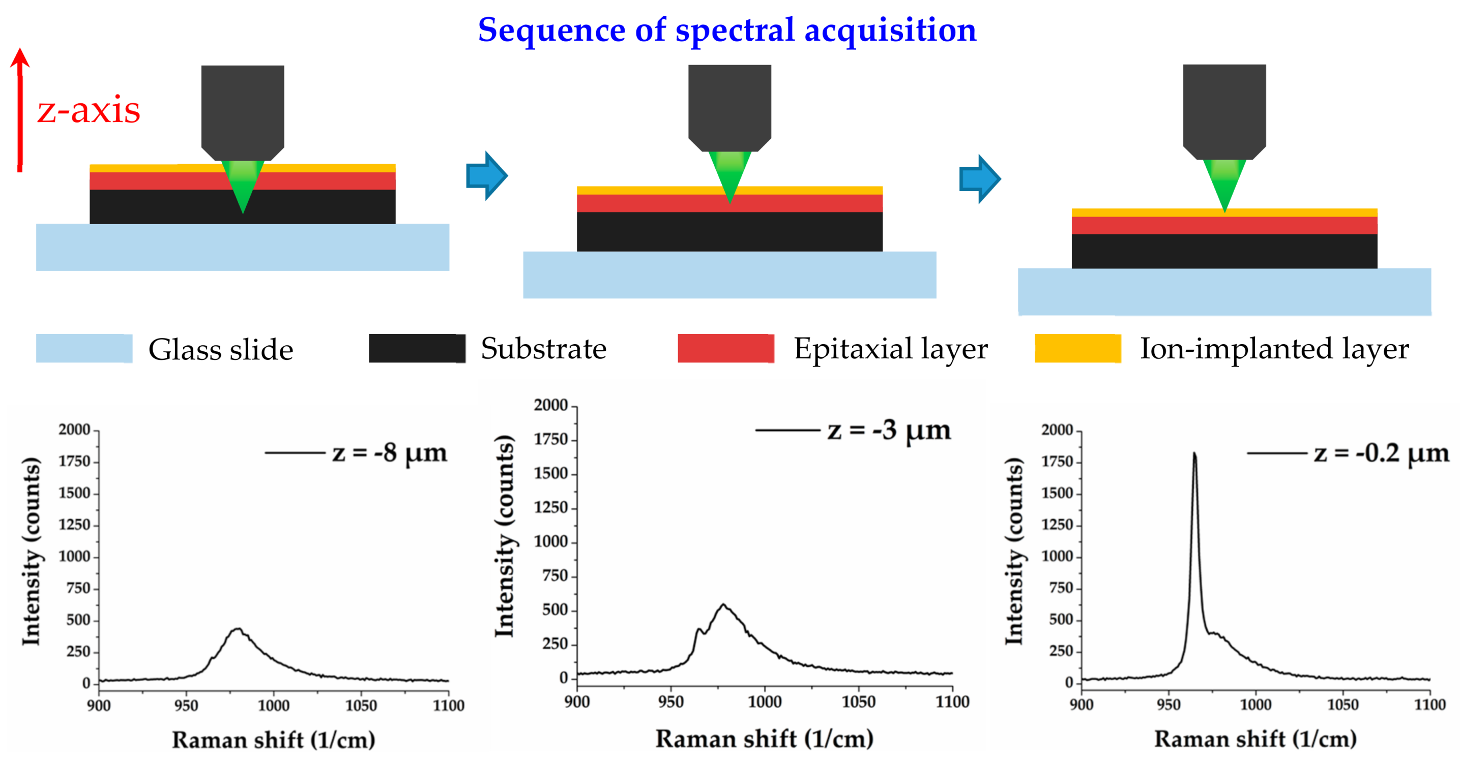
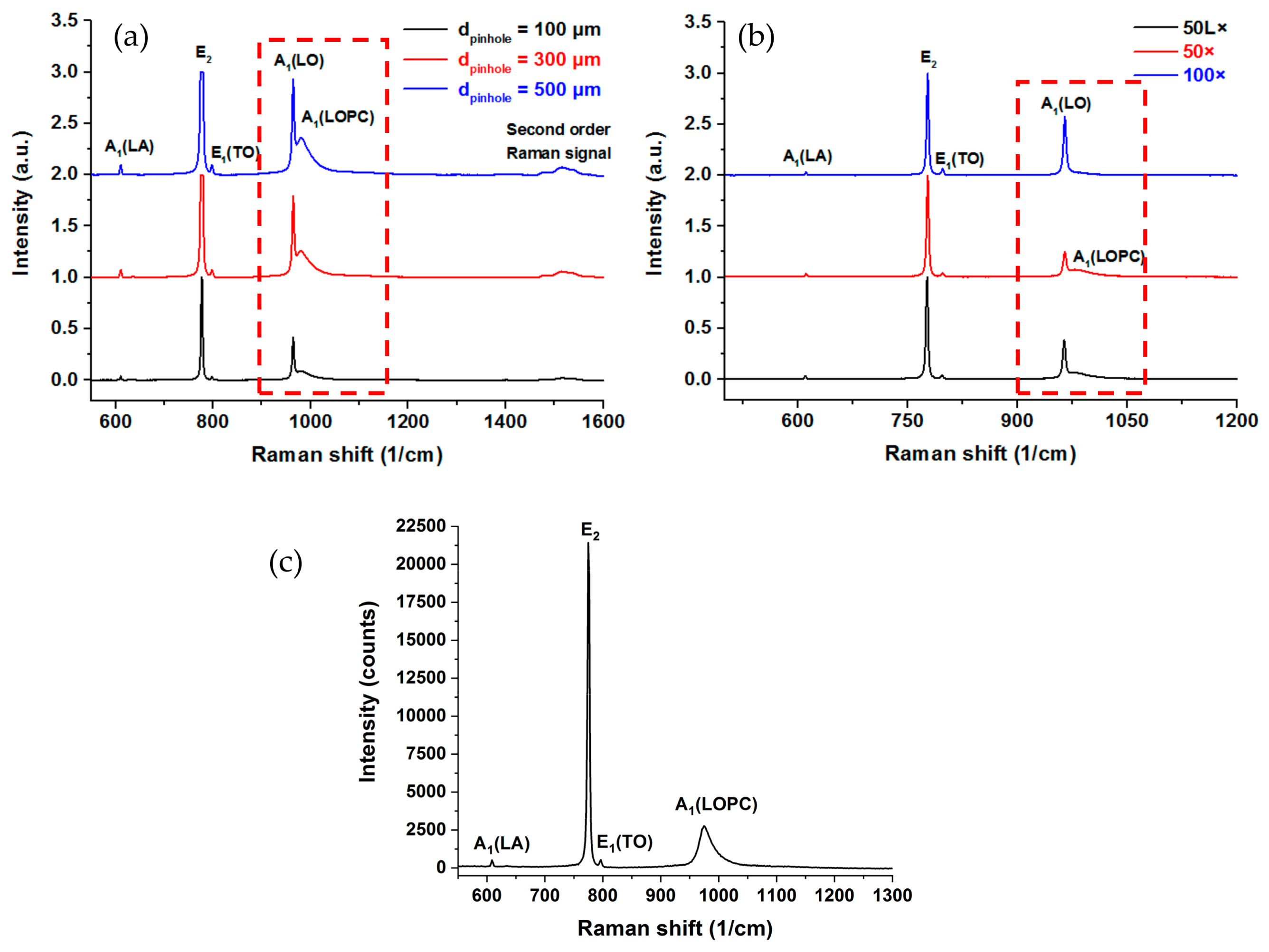
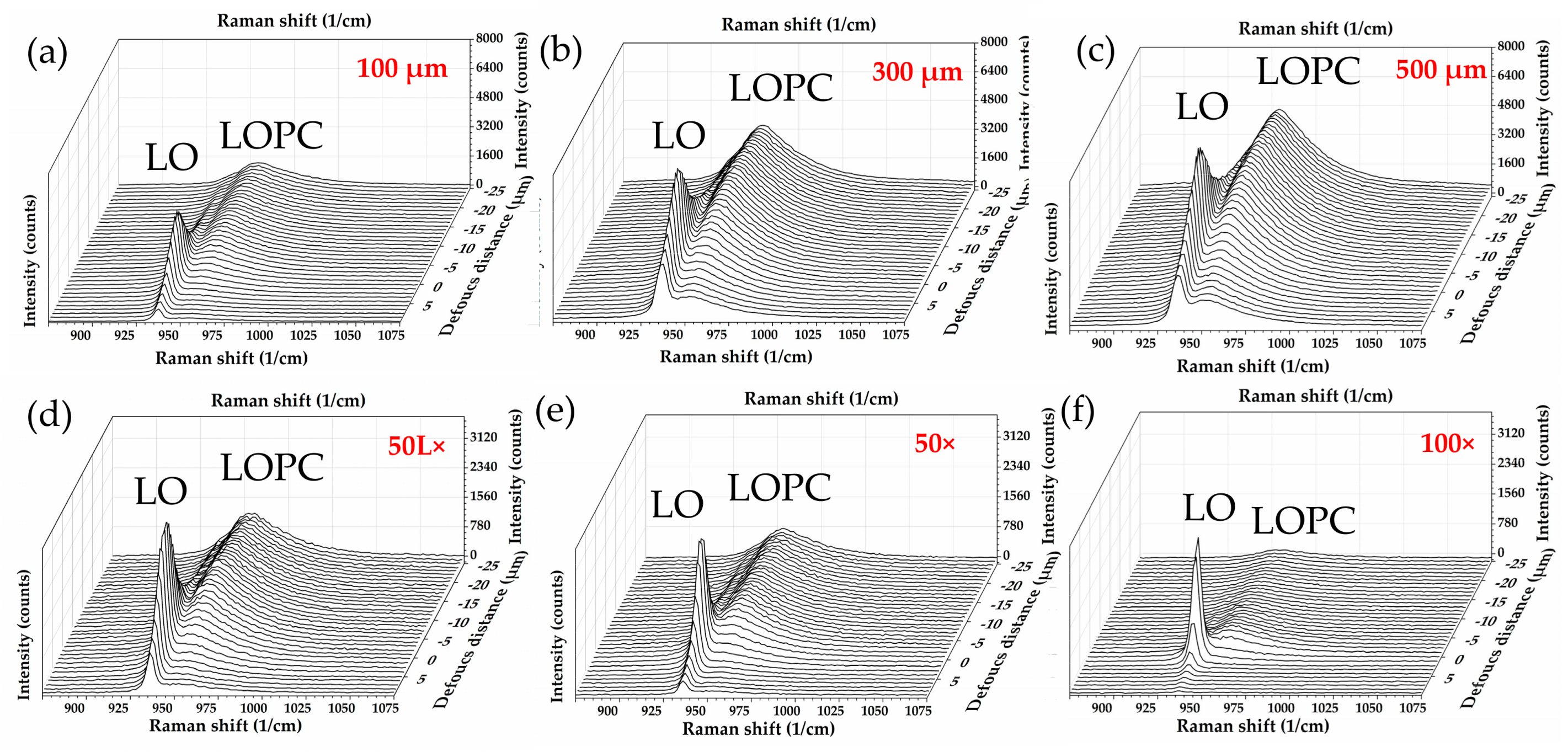
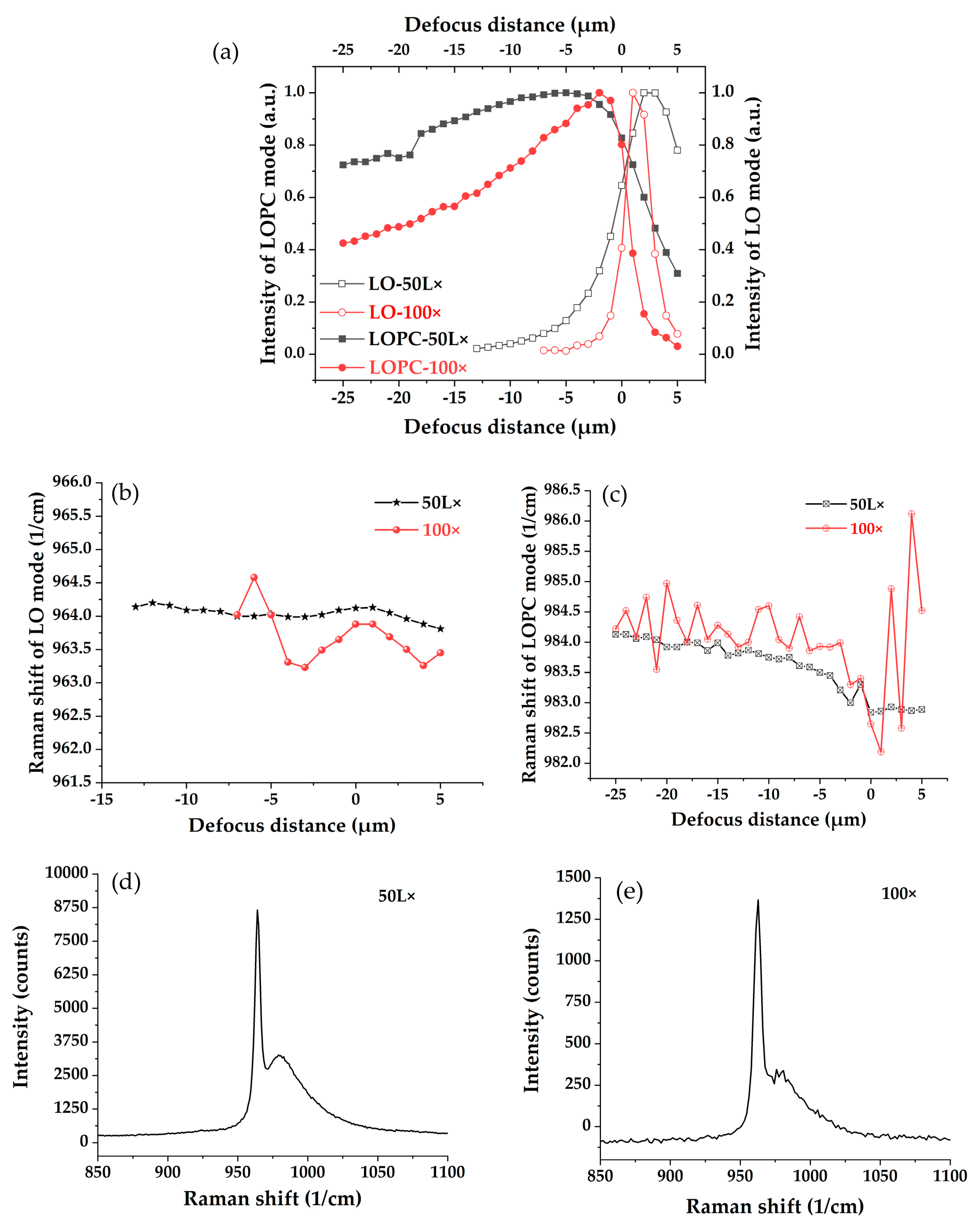
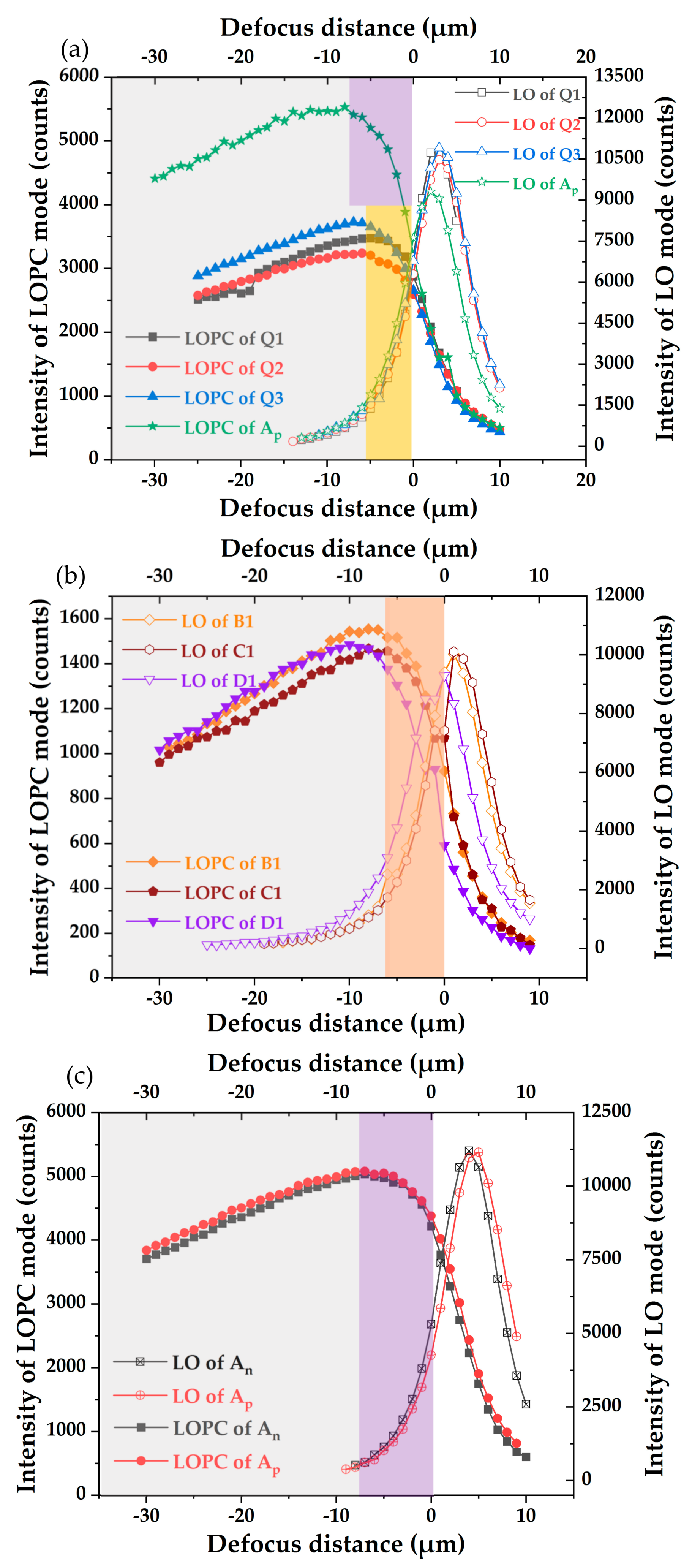
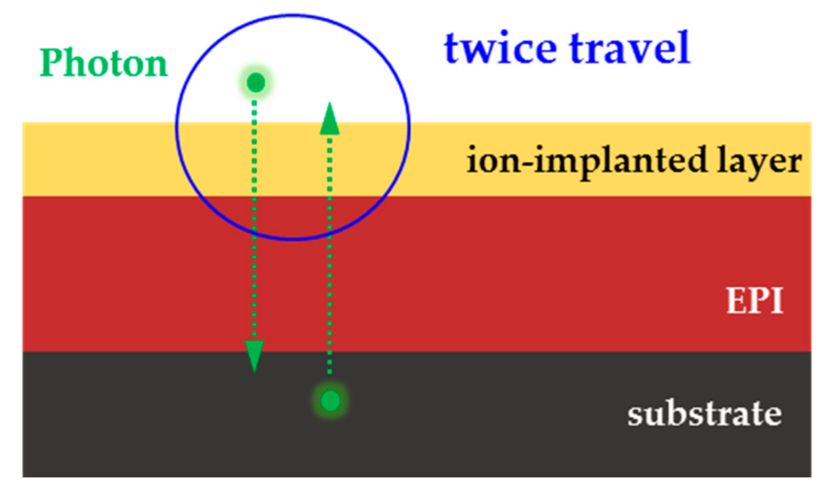
3.1. Depth Profiling Set-Ups

The selection of measurement parameters has a significant impact on the data fitting and analysis. For depth profiling of a multilayer structure, both spatial resolution and signal intensity need to be considered. As is well known, the lateral resolution of a Raman microscope is directly related to the laser spot size, which is mostly governed by the laser wavelength and the N.A. of the objective lens. Except for these factors that determine the lateral resolution, the size of the confocal pinhole influences the depth resolution significantly. The micro scale pinhole placed in the back image plane filters most of the scattered light from outside the focal plane to obtain an optimized depth resolution. Furthermore, the sample characteristics, especially the refractive index and absorption coefficient, also have a remarkable impact on the depth resolution of the system [12,19].
To evaluate the depth resolution of the measurement system, depth profiling with different pinholes and different lenses was studied using sample Q1 processed by Al ion-implantation with a surface concentration of 5 × 1016 cm−3 followed by annealing at 1700 °C for 30 minutes (Table 1). After calibrating the spectrometer using a silicon chip under the condition of 532 nm laser excitation, single spectra of Q1 with different pinhole sizes and lenses were collected focusing on the surface of the sample, as shown in Figure 3a,b. In the backscattering geometric configuration, A1 modes (longitudinal acoustic mode (LA mode) at 610 cm−1, LO mode at 964 cm−1, and LOPC mode at ~980 cm−1), E2 mode at 776 cm−1, E1 mode at 797 cm−1, and the second order Raman peaks can be observed. The spectra showed two overlapping peaks in the range of 950–1000 cm−1 (framed with red dashed lines in Figure 3a,b, which were the longitudinal optical mode (LO mode) located at 964 cm−1 and the LOPC peak located at around 980 cm−1 [20], respectively. As the diameter of the confocal pinhole becomes smaller or the numerical aperture of the objective lens becomes larger, the LOPC peak information is filtered out more, so the LOPC information is assumed to be derived from the substrate of the sample. Pinholes with diameters of 300 μm and 500 μm exhibit a similar intensity ratio because the true confocal mode is only available when the pinhole diameter is less than 200 μm. The objective lens with large N.A. corresponds to a smaller entrance pupil size, which filters more information from the substrate, thus shows a much weaker LOPC mode. To further confirm the origin of the LOPC mode, a Raman spectrum of the heavily doped n-type 4H–SiC substrate without epitaxial growth was measured and is shown in Figure 3c. For the substrate, only the LOPC peak can be observed at around 978 cm−1, which is estimated to correspond to a carrier concentration of 2.7 × 1018 cm−3 [21].
The distribution of the Raman signal in the depth direction (along the z-axis) is shown in Figure 4, which corresponded well to the multilayer structure of the sample. When focusing on the substrate layer (negative defocus distance), no LO peak appeared, whereas an obvious LOPC peak was observed. When the focal plane moved toward the surface of the sample (which corresponded to 0 for the defocus distance), the LO peak gradually appeared and the LOPC peak decreased. Thus, we classified the LO peak as the longitudinal optical mode (LO mode) of the epitaxial layer and the LOPC peak as the longitudinal optical phonon-plasmon coupled mode (LOPC mode) of the heavily doped substrate, respectively. Druy et al. arrived at similar conclusions [16]. Figure 4a–c indicate that the distribution of the LO peak along the depth direction had a narrower width for smaller pinholes, which implies a stronger ability to distinguish multilayer structures for smaller pinholes. Figure 4d–f show that the distribution of the LO peak intensity along the depth direction was very steep for the 100× lens due to the higher spatial resolution of the objective lens with a large numerical aperture.
To compare the depth profiling results using different objective lenses, the authors compared the results of the 50L× and 100× objective lenses and 100 μm pinhole with the z-scanning step of 1 μm. Figure 5 shows the LO mode and LOPC mode distributions in the depth direction after normalization with the intensity maximum. As shown in Figure 5a, the signal intensity of the 100× objective lens changed steeply, showing its high spatial resolution. When comparing the peak position of LO and LOPC mode in Figure 5b,c, the results of the 50L× lens had a better coherence and showed a more stable regular change. Spectra when focusing on the sample surface in Figure 5d,e showed that the luminous flux of the 100× objective lens was smaller and the signal-to-noise ratio of the signal was worse than that for the 50L× lens. Therefore, for the 100× lens, the fitting error was larger than that for the spectra measured with the 50L× lens, which was not conducive to the analysis of the subsequent laws of LO and LOPC mode position for the depth profiling.

3.2. Determination of Epitaxial Thicknesses by Depth Profiling

Depth profiling can distinguish the LOPC and LO signal from the substrate and the epitaxial layer. Considering the high depth resolution of the 100× lens (Table 2), depth profiling experiments were first performed using the 100× lens, as shown in Figure 6a. The LOPC peak began to decrease at around −2 to −3 μm, which is shallower than the actual position of the interface between the substrate and epitaxial layer (Table 1), with deviations of around 3 to 4.5 μm. This phenomenon conforms to the law of refraction. Silicon carbide has a large refractive index of 2.68 at the laser wavelength. As shown in Figure 6b,c for the 100× lens, which has a large half-entrance angle θ of 64.2°, the actual focus point (Z’) caused by refraction would be much deeper than the theoretical focus point Z (controlled by the positioning of Z-axis sample stage) without considering the influence of refraction. Therefore, although the 100× lens has the best depth resolution in principle, because of its large angle of incidence, the large depth deviation of the actual focal point caused by refraction will degrade its depth characterization performance to some extent.
As shown in Figure 7, for samples with different epitaxial thicknesses, the inflection point at which the LOPC intensity began to decrease was close to the interface of the substrate and the epitaxial layer using the 50L× lens. The thicknesses of the epitaxial layers are shown in Table 1, which were measured by FTIR (Fourier-transform infrared spectroscopy) measurements [22,23,24,25]. The inflection point was determined using the depth at which the maximum intensity of the LOPC mode appeared (negative defocus distance). Multiple measurements (at least five times) with a depth step of 0.5 μm were performed on the same epitaxial layer. The mean position of the maximum of the LOPC peak intensity x and the standard deviation of the mean σx were calculated. The deviation (Δ = x – Th epi) between the average position of the LOPC peak maximum (x) and the real interface position measured by FTIR (Th epi) are listed in Table 3. The deviations were distributed in the range of −1.2~−1.7 μm. For the three kinds of thicknesses for the epitaxial layer (5.3 μm, 6 μm, and 7.5 μm), the average deviations of the Raman depth analyses were −1.7 μm, −1.2 μm, and −1.4 μm, respectively. The standard deviation of the average position was between 0.1 μm and 0.5 μm. Furthermore, it should be noted that, in the actual sample, there is a buffer layer between the substrate layer and the epitaxial layer with a thickness of ~0.5 μm. The presence of the buffer layer may be a cause of the deviation in the results.
Thus, the thickness of the epitaxial layer can be determined by the inflection point at which the LOPC peak intensity reaches the maximum with deviations of –1.7 μm, –1.2 μm, and –1.4 μm for epitaxial layer thicknesses of 5.3 μm, 6 μm, and 7.5 μm. Therefore, depth profiling with a 50L× lens is an effective approach to determine the thickness of the epitaxial layer with deviations of –1.2~–1.7 μm.
Compared with the depth profiling results, the thickness of the epitaxial layer could be better characterized by the 50L× lens with smaller deviations. Two key parameters of the objective lens can well explain the above results. On one hand, the smaller angle of incidence θ for the 50L× lens (Table 2) reduced the refraction influence. The length of the laser beam waist, which is also called the depth of focus ω [11], is shown in Table 2 and Figure 6b. ω is usually defined as Equation (1).
ω = 6.4   × λ 2 π × ( 1 t a n θ ) 2 λ × ( 1 t a n θ ) 2
where λ is the wavelength of the incident laser and θ is the half-entrance angle of the objective lens. On the other hand, the 50L× lens has a larger depth of focus (Table 2), which can compromise the refraction influence on depth profiling to some extent.

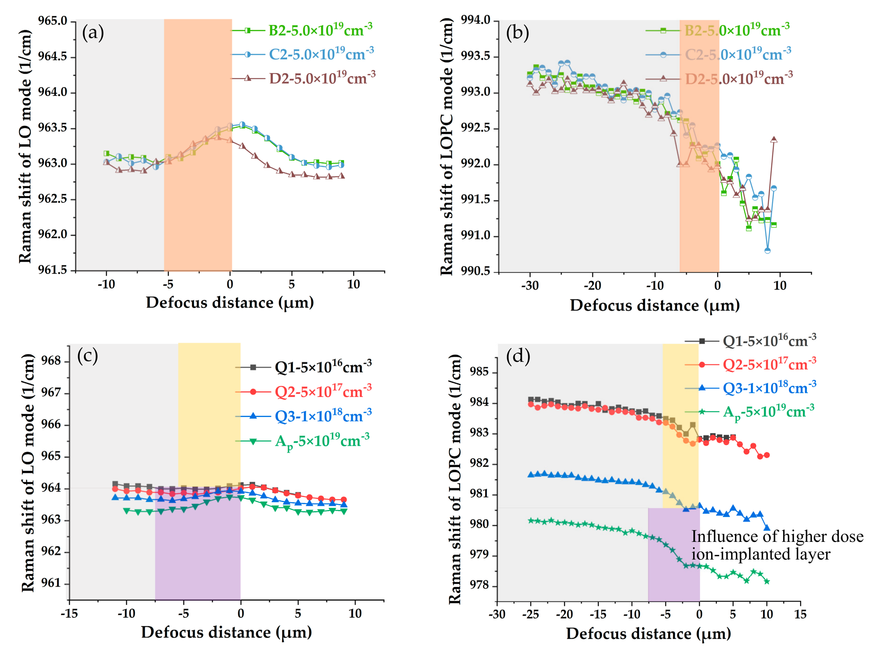
3.3. Depth Profiling of Net Doping Concentration

The above analysis identified the overlap of the LO and LOPC mode related peaks in the range of 950–1000 cm−1. Furthermore, we aimed to extract the information of the nanoscale surface layer being modified by ion-implantation and annealing from the Raman depth analysis. Depth profiling of the samples in Table 1 with different carrier concentrations and different annealing treatments were studied. The variation of the LO and LOPC peak position with nominal focus position (also called the defocus distance in this paper) in Figure 8 were excited by 532 nm laser using 100 μm pinhole and the 50L× lens, where the gray blocks represent the substrates and the different colored blocks represent the epitaxial layers of different samples (according to the data in Table 1).
The results in Figure 8a,b, which have the same coordinate scale showed that the LO peak position in all regions was relatively stable, fluctuating within 0.5 cm−1, while the LOPC peak showed a blue shift of around 1.5 cm−1 in the depth direction between −30 µm and the 0 µm defocus distance. Similarly, in Figure 8c,d, the LO peak position showed a line shift no more than 0.5 cm−1 and the LOPC peak showed a blue shift of 1.0–1.5 cm−1 from the substrate to the sample surface. The Raman shift of the LOPC peak was relatively stable when focusing on the substrate and above the surface of the sample. In contrast, a manifest blue shift was observed when the focal plane moved from the interface of the substrate layer and the epitaxial layer to the surface of the sample (between −7.5/−6/−5.3 µm and 0 µm defocus distance). Many studies have shown the sensitivity of the LOPC mode on carrier concentration of the n-type 4H–SiC [26,27,28,29,30]. The heavily doped n-type substrates had relatively high carrier concentrations in the orders of 1018 cm−3, while the n-type epitaxial layers had rather low carrier concentrations of ≈1.0 × 1016 cm−3 comparatively. When focusing on the substrate, most of the signal was from the substrate layer, so the LOPC peak position was relatively stable. When the focusing point moved from the substrate to the epitaxial layer, the apparent difference in carrier concentration between the substrate (~1018 cm−3) and the epitaxial layer (~1016 cm−3) led to a blue shift in the LOPC peak. As the sampling volume was not infinitely small, the change in LOPC peak position was not as steep as the change in carrier concentration. Furthermore, the buffer layer, which had a carrier concentration lower than the substrate and higher than the epitaxial layer, also led to a smoother transition of the LOPC peak position from the substrate to the epitaxial layer. Thus, the blue shift in the depth direction of the LOPC mode can be attributed to the carrier concentration gradient from the substrate to the epitaxial layer. Additionally, the different annealing process parameters did not result in a significant difference in the peak positions of the LOPC mode. In addition, when comparing the frequency shift of the LOPC peak position among samples with different thicknesses of the epitaxial layer such as sample A and Q1/Q2/Q3 in Figure 8d, a greater blue shift around 1 cm−1 in the depth direction was found for sample A, which had a thicker epitaxial layer.
For samples Q1, Q2, and Q3, the LOPC mode relationships in Figure 8d corresponded well to our previous single Raman spectrum results focusing on the sample surface [20]: when the surface Al carrier concentration was equal or larger than 1018 cm−3 (i.e., Q3), the LOPC mode showed a blue shift whereas no apparent difference was found in the LOPC peak position between Q1 and Q2.
Furthermore, samples Q1, Q2, and Q3 had exactly the same substrates and epitaxial layers and only differed in the implantation dose, thus the same LOPC mode position of the substrate was expected to be seen for Q1, Q2, and Q3. However, the LOPC peaks position were different when focusing on both the substrates and the epitaxial layers. From the comparison of the processing of Q1, Q2, and Q3, the only reason for the difference in the LOPC peak position was the different ion-implantation treatments. After the exciting photons reach the substrate layer, they carry the information of the substrate and scatter to the sample surface and reach the detector. In this process, photons from substrate layers travel twice through the surface modified layer (ion-implanted layer), as shown in Figure 9. Since the LOPC mode is sensitive to the carrier concentration, the twice travel of the photons through the p-type (hole-conducting) surface modified layer will bring inevitable influence from the p-type ion-implanted layer. The differences were evident between the LOPC positions of the Q1 and Q2 peaks (which were very similar) and the Q3 peaks. We believe that the second coupling of those photons (from the substrate layers) and the hole carriers in the surface Al ion-implanted layers led to the difference in the LOPC peak position of Q1, Q2, and Q3.

4. Conclusions

The confocal Raman depth profiling method is a fast and non-destructive method to obtain the electrical properties profiling of ion-implanted silicon carbide in the depth direction. The results of the depth analysis corresponded well to the surface single-point spectra we reported earlier and provides plentiful information on the following. (1) Raman spectra distribution in the depth direction identified the LO mode as the longitudinal optical mode (LO mode) as representative for the epitaxial layer and the longitudinal optical phonon-plasmon coupled mode (LOPC mode) as representative for the heavily doped substrate, respectively. (2) The epitaxial layer thickness could be evaluated according to the intensity variation of the LOPC peak in the depth direction from the position of the maximum of the LOPC peak intensity. For three kinds of thicknesses for the epitaxial layer (5.3 μm, 6 μm, and 7.5 μm), the average deviations of the according Raman depth analysis were −1.7 μm, −1.2 μm, and −1.4 μm, respectively. (3) For ion-implanted 4H–SiC samples, the apparent difference in carrier concentration between the substrate (~1018 cm−3) and the epitaxial layer (~1016 cm−3) led to a blue shift in the LOPC peak along the depth direction (from the substrate to the epitaxial layer). A greater blue shift was found for the thicker epitaxial layer of sample A. (4) The twice travel (excitation and collection) of photons from the substrate resulted in a second coupling with the surface ion-implanted layer, which led to the difference in the LOPC peak position of Q1, Q2, and Q3.
Furthermore, the depth profiling results with different sized pinholes and lenses showed that the 100 μm sized pinhole and 50L× lens were more suitable to undertake the depth analysis of the 4H–SiC substrate with an epitaxial layer of several micrometers in thickness and a top layer in the nanoscale, considering both the depth resolution, signal to noise ratio, and refraction effect.

Supplementary Materials

The following are available online at https://www.mdpi.com/2073-4352/10/2/131/s1, Figure S1: The fitting results of 50L× lens at +5 μm and 100× lens at +1 μm, Figure S2: The spectra of sample A p, Q1, and B2, Figure S3: Detailed fitting results for samples A p, Q1, and B2; Table S1: Fitting error (with respect to the peak positions) of sample A p, Q1, and B2 when Z = 0.

Author Contributions

Y.S. performed all the experiments, Y.S. and Z.X. conceived and designed the layout; Z.X., M.R., and H.W. collected and contributed materials; Z.X., M.R., T.L., H.W., Y.W., and F.F. provided valuable discussions and suggestions for the paper; Y.S., Z.X., and T.L. wrote the paper. All authors have read and agreed to the published version of the manuscript.

Funding

The study was supported by the National Natural Science Foundation of China (No. 51575389, 51761135106), the National Key Research and Development Program of China (2016YFB1102203), the State Key Laboratory of Precision Measuring Technology and Instruments (Pilt1705), and the ‘111’ project by the State Administration of Foreign Experts Affairs and the Ministry of Education of China (Grant No. B07014).

Conflicts of Interest

The authors declare no conflicts of interest.

References

  1. Zhu, L.P.; He, H.P. Wide Band Gap Compound Semiconductor Materials and Devices; Zhejiang University Press: Hangzhou, China, 2016. [Google Scholar]
  2. Campos, F.J.; Mestres, N.; Alsina, F.; Pascual, J.; Morvan, E.; Godignon, P.; Millán, J. Confocal micro-Raman scattering and Rutherford backscattering characterization of lattice damage in aluminum implanted 6H–SiC. Diam. Relat. Mater. 1998, 8, 357–360. [Google Scholar] [CrossRef]
  3. Schöner, A.; Karlsson, S.; Schmitt, T.; Nordell, N.; Linnarsson, M.; Rottner, K. Hall Effect Investigations of 4H–SiC Epitaxial Layers Grown on Semi-Insulating and Conducting Substrates. Mater. Sci. Eng. B 1999, 61, 389–394. [Google Scholar] [CrossRef]
  4. Fukuda, Y.; Nishikawa, K.; Shimizu, M.; Iwakuro, H. Point-Contact Current Voltage Technique for Depth Profiling of Dopants in Silicon Carbide. Mater. Sci. Forum 2002, 389–393, 671–674. [Google Scholar] [CrossRef]
  5. Chandra, N.; Sharma, V.; Chung, G.Y.; Schroder, D.K. Four-point probe characterization of 4H silicon carbide. Solid State Electron. 2011, 64, 73–77. [Google Scholar] [CrossRef]
  6. Sherbondy, J.; Hillard, R. Process characterization of low-dose, threshold-voltage adjust channel implants using mercury-probe capacitance–voltage measurements. J. Vac. Sci. Technol. B Microelectron. Nanometer Struct. 2000, 18, 450–453. [Google Scholar] [CrossRef]
  7. Österman, J.; Hallén, A.; Anand, S.; Linnarsson, M.K.; Andersson, H.; Åberg, D.; Panknin, D.; Skorupa, W. Techniques for Depth Profiling of Dopants in 4H-SiC. Mater. Sci. Forum 2001, 353–356, 559–562. [Google Scholar] [CrossRef]
  8. Stutz, C.E. Photoelectrochemical Capacitance-Voltage Measurements of 4H-SiC. J. Electron. Mater. 1998, 27, L81–L83. [Google Scholar] [CrossRef]
  9. Czett, A.; Buday, C.; Savtchouk, S.; Marinskiy, D. Non-contact high precision alternative to Hg-probe for dopant profiling in SiC. Phys. Status Solidi (c) 2014, 11, 1601–1605. [Google Scholar] [CrossRef]
  10. Giannazzo, F.; Calcagno, L.; Raineri, V.; Ciampolini, L.; Ciappa, M.; Napolitani, E. Quantitative carrier profiling in ion-implanted 6H–SiC. Appl. Phys. Lett. 2001, 79, 1211–1213. [Google Scholar] [CrossRef]
  11. Linnarsson, M.K.; Hallén, A.; Vines, L. Intentional and unintentional channeling during implantation of 51V ions into 4H-SiC. Semicond. Sci. Technol. 2019, 34, 115006. [Google Scholar] [CrossRef]
  12. Tabaksblat, R.; Meier, R.J.; KIP, B.J. Confocal Raman Microspectroscopy: Theory and Application to Thin Polymer Samples. Appl. Spectrosc. 1992, 46, 60–68. [Google Scholar] [CrossRef]
  13. Brink, D.J.; Maurice, T.; Blanque, S.; Kunert, H.; Camassel, J.; Pascual, J. Depth profiling of high energy hydrogen-implanted 6H-SiC. Appl. Opt. 2004, 43, 1275–1280. [Google Scholar] [CrossRef] [PubMed]
  14. Campos, F.J.; Mestres, N.; Pascual, J.; Morvan, E.; Godignon, P.; Millán, J. Confocal micro-Raman characterization of lattice damage in high energy aluminum implanted 6H-SiC. J. Appl. Phys. 1999, 85, 99–104. [Google Scholar] [CrossRef]
  15. Żuk, J.; Romanek, J.; Skorupa, W. Micro-Raman depth profile investigations of beveled Al+-ion implanted 6H-SiC samples. Nucl. Instrum. Methods Phys. Res. Sect. B Beam Interact. Mater. At. 2009, 267, 1251–1254. [Google Scholar] [CrossRef]
  16. De Biasio, M.; Kraft, M.; Schultz, M.; Goller, B.; Sternig, D.; Esteve, R.; Roesner, M. Micro-Raman spectroscopy as a tool for the characterization of silicon carbide in power semiconductor material processing. Next-Gener. Spectrosc. Technol. X 2017, 10210, 1021014. [Google Scholar] [CrossRef]
  17. Liu, T.; Xu, Z.; Rommel, M.; Wang, H.; Song, Y.; Wang, Y.; Fang, F. Raman Characterization of Carrier Concentrations of Al-implanted 4H-SiC with Low Carrier Concentration by Photo-Generated Carrier Effect. Crystals 2019, 9, 428. [Google Scholar] [CrossRef] [Green Version]
  18. Kocher, M.; Rommel, M.; Erlbacher, T.; Bauer, A.J. Influence of Al Doping Concentration and Annealing Parameters on TiAl Based Ohmic Contacts on 4H-SiC. Mater. Sci. Forum 2018, 924, 393–396. [Google Scholar] [CrossRef]
  19. Everall, N.J. Modeling and measuring the effect of refraction on the depth resolution of confocal Raman microscopy. Appl. Spectrosc. 2000, 54, 773–782. [Google Scholar] [CrossRef]
  20. Xu, Z.W.; Song, Y.; Rommel, M.; Liu, T.; Kocher, M.; He, Z.D.; Wang, H.; Yao, B.T.; Liu, L.; Fang, F.Z. Raman Spectroscopy Characterization of Ion Implanted 4H-SiC. Mater. Sci. Forum 2019, 963, 424–428. [Google Scholar] [CrossRef]
  21. Harima, H.; Nakashima, S.i.; Uemura, T. Raman scattering from anisotropic LO-phonon–plasmon–coupled mode in n-type 4H– and 6H–SiC. J. Appl. Phys. 1995, 78, 1996–2005. [Google Scholar] [CrossRef]
  22. Macmillan, M.F.; Henry, A.; Janzén, E. Thickness Determination of Low Doped SiC Epi-Films on Highly Doped SiC Substrates. J. Electron. Mater. 1998, 27, 300–303. [Google Scholar] [CrossRef]
  23. Oishi, S.; Hijikata, Y.; Yaguchi, H.; Yoshida, S. Simultaneous Determination of Carrier Concentration, Mobility, and Thickness of SiC Homoepilayers by Infrared Reflectance Spectroscopy. Jpn. J. Appl. Phys. 2006, 45, L1226–L1229. [Google Scholar] [CrossRef]
  24. Li, Z.Y.; Sun, J.W.; Zhang, Y.M.; Zhang, Y.M.; Tang, X.Y. Methods for Thickness Determination of SiC Homoepilayers by Using Infrared Reflectance Spectroscopy. Chin. Phys. Lett. 2010, 27, 068103. [Google Scholar]
  25. Dong, L.; Sun, G.-S.; Zheng, L.; Liu, X.-F.; Zhang, F.; Yan, G.-G.; Zhao, W.-S.; Wang, L.; Li, X.-G.; Wang, Z.-G. Characterization of 4H–SiC substrates and epilayers by Fourier transform infrared reflectance spectroscopy. Chin. Phys. B 2012, 21, 047802. [Google Scholar] [CrossRef]
  26. Müller, R.; Künecke, U.; Thuaire, A.; Mermoux, M.; Pons, M.; Wellmann, P. Investigation of the charge carrier concentration in highly aluminum doped SiC using Raman scattering. Phys. Status Solidi (c) 2006, 3, 558–561. [Google Scholar] [CrossRef]
  27. Fukasawa, R.; Perkowitz, S. Raman-scattering spectra of coupled LO-phonon-hole-plasmon modes in p-type GaAs. Phys. Rev. B Condens. Matter. 1994, 50, 14119–14124. [Google Scholar] [CrossRef]
  28. Harima, H.; Hosoda, T.; Nakashima, S. Carrier Density Evaluation in P-Type SiC by Raman Scattering. Mater. Sci. Forum 2000, 338–342, 607–610. [Google Scholar] [CrossRef]
  29. Nakashima, S.; Kitamura, T.; Mitani, T.; Okumura, H.; Katsuno, M.; Ohtani, N. Raman scattering study of carrier-transport and phonon properties of 4H−SiC crystals with graded doping. Phys. Rev. B 2007, 76, 245208. [Google Scholar] [CrossRef]
  30. Caldwell, J.D.; Glembocki, O.J.; Prokes, S.M.; Glaser, E.R.; Hobart, K.D.; Hansen, D.M.; Chung, G.; Bolotnikov, A.V.; Sudarshan, T.S. Free carrier distribution profiling of 4H-SiC substrates using a commercial optical scanner. J. Appl. Phys. 2007, 101, 093506. [Google Scholar] [CrossRef]
Figure 1. Schematic of the ion-implanted multi-layer samples (not drawn by scale in order to show the multi-layer structure clearly).
Crystals 10 00131 g001
Figure 2. (Top) Schematic of the depth profiling (not drawn to scale in order to show the multilayer structure clearly). (Bottom) Raman spectra of the Al-doped sample A obtained by the 532 nm excitation line and 2400 lines/mm grating with the 100× lens at different focal planes, corresponding to Raman signals from the three different layers. The step of depth profiling is 0.2 μm. The origin of the z-axis (z = 0 μm) is located at the top of ion-implanted layer.
Crystals 10 00131 g002
Figure 3. Raman spectra of sample Q1 for different pinhole sizes and different lenses (the spectra are normalized to E2 mode intensity) and the single spectrum of heavily doped 4H–SiC substrate: (a) Single spectra of Q1 with a confocal pinhole of 100 μm, 300 μm, and 500 μm using a 50L× lens and grating of 1800 lines/mm; (b) Single spectra of Q1 with lenses of 50L×, 50×, and 100× using a 100 μm pinhole, and grating of 2400 lines/mm; (c) Single spectrum of 4H–SiC substrate without an epitaxial layer with lens of 50L×, a 100 μm pinhole, and grating of 1800 lines/mm.
Crystals 10 00131 g003
Figure 4. Depth profiling of sample Q1 with different pinhole sizes (a–c) and lenses with different N.A. (d–f): (a) was obtained by 50L× and 100 μm pinhole; (b) was obtained by 50L× and 300 μm pinhole; (c) was obtained by 50L× and 500 μm pinhole; (d) was obtained by 50L× (long working distance objective lens) and 100 μm pinhole; (e) was obtained by 50× and 100 μm pinhole; (f) was obtained by 100× and 100 μm pinhole. The step of depth profiling is 1 μm.
Crystals 10 00131 g004
Figure 5. (a–c): Variation of peak intensity (a) and position (b,c) of sample Q1 with lenses of 50L× and 100× using a 100 μm pinhole. The step of depth profiling is 1 μm. (d) Raman spectrum of Q1 when focusing on the sample surface using the 50L× lens. (e) Raman spectrum of Q1 when focusing on the sample surface using the 100× lens. The fitting procedure always converged and resulted in a R2 (coefficient of determination) in the range of 0.973–0.998. In the whole range of depth profiling, the standard error of the LOPC mode position is between 0.19–0.25 cm−1 and for LO mode, the standard error of peak position is between 0.01–0.25 cm−1 (Supplementary Materials).
Crystals 10 00131 g005
Figure 6. (a) Variation of the LO and LOPC peak position with the defocus distance using the 100× lens (for sample Q1, Q2, and Ap). The step of depth profiling is 1 μm. (b) Schematic diagram of the objective lens. (c) Schematic diagram of the refraction on the SiC substrate in depth profiling when using the 100× lens.
Crystals 10 00131 g006
Figure 7. The variation of the LO and LOPC mode peak intensities with the defocus distance using the 50L× lens, in which the gray blocks represent the substrates and the different colored blocks represent the epitaxial layers of different samples according to Table 1: (a) LO and LOPC mode intensity distribution in the depth direction of A p and Q; (b) LO and LOPC mode intensity distribution in the depth direction of B1, C1, and D1; (c) LO and LOPC mode intensity distribution in the depth direction of A n and A p. The step of depth profiling is 1 μm.
Crystals 10 00131 g007
Figure 8. The variation of the LO and LOPC peak position with the defocus distance, in which gray blocks represent the substrates and the different colored blocks represent the epitaxial layers of different samples (according to Table 1): (a) LO mode distribution along z-axis of B2, C2, and D2; (b) LOPC mode distribution along the z-axis of B2, C2, and D2. (c) LO mode distribution along the z-axis of A p, Q1, Q2, and Q3; (d) LOPC mode distribution along the z-axis of A p, Q1, Q2, and Q3. The step of depth profiling is 1 μm. The fitting procedure always converged. For Figure 8a,b in the whole range of depth profiling, the R2 (coefficient of determination) was in the range of 0.964–0.998; the standard error of LOPC mode position was in the range of 0.31–0.46 cm−1, and the standard error of the LO mode peak position was between 0.01–0.15 cm−1. For Figure 8c,d in the whole range of depth profiling, the R2 was in the range of 0.973–0.999; the standard error of the LOPC mode position was between 0.14–0.25 cm−1 and for the LO mode, the standard error of peak position was between 0.01–0.25 cm−1.
Crystals 10 00131 g008
Figure 9. The schematic of the twice travel of photons excited from the substrate.
Crystals 10 00131 g009
Table 1. Details of the samples used in Raman characterization.
SampleEpitaxyImplantationAnnealing
LabelCarrier Concentration (cm−3)Thickness (μm)ElementSurface Concentration (cm−3)Temperature (°C)Time (min)
G≈6.0 × 10¹⁵≈5.3-a-1700 30
Q1≈6.0 × 10¹⁵ ≈5.3Al5.0 × 10161700 30
Q2≈6.0 × 10¹⁵ ≈5.3Al5.0 × 10171700 30
Q3≈6.0 × 10¹⁵ ≈5.3Al1.0 × 10181700 30
A≈1.4 × 10¹⁶ ≈7.5N5.0 × 10191700 30
≈1.4 × 10¹⁶≈7.5Al5.0 × 1019170030
B1≈1.0 × 10¹⁶ ≈6Al3.3 × 1018170030
B2≈1.0 × 10¹⁶≈6Al5.0 × 10191700 30
C1≈1.0 × 10¹⁶ ≈6Al3.3 × 10181800 30
C2≈1.0 × 10¹⁶ ≈6Al5.0 × 10191800 30
D1≈1.0 × 10¹⁶≈6Al3.3 × 10181900 1
D2≈1.0 × 10¹⁶ ≈6Al5.0 × 10191900 1
Sub b------
a No ion-implantation was performed in this area. Thus, no surface concentration is given. b Substrate material without epitaxial growth from Xiamen Powerway Advanced Material Co. Ltd. (PAM-XIAMEN).
Table 2. The depth resolution of a confocal Raman microscope as a function of objective lens and pinhole diameter [12].
ObjectiveN.A. aWD b (mm)Half-Entrance Angle θ c (deg)Depth of Focus ω (μm)Pinhole Diameter (μm)
500300100
Depth Resolution d (μm)
50×0.750.3748.60.46.03.01.5
50L× e0.510.630.01.6148.03.0
100×0.90.2164.20.13.01.20.7
a Numerical aperture. b Working distance. c Half-entrance angle θ = sin−1(N.A.). d The values have been multiplied by two to obtain the total depth where Raman signal originates from (above and below the focal plane). e Long working distance objective.
Table 3. The interface position measured by FTIR measurements, average position of the maximum of LOPC peak intensity, and the deviations of the Raman depth profiling for samples with three kinds of epitaxial thicknesses. The step of depth profiling is 0.5 μm.
LabelInterface Position Measured by FTIR (Thepi/μm)Average Position of LOPC Intensity maximum (x/μm)Standard Deviation of the Average Position (δx/μm)Deviation of Raman Depth Profiling (Δ/μm)
Q1–5.3–7.10.4–1.8
Q2–5.3–6.30.4–1.0
G–5.3–7.60.1–2.3
B1–6.0–6.70.2–0.7
B2–6.0–7.90.1–1.9
C1–6.0–7.00.5–1.0
An–7.5–8.60.4–1.1
Ap–7.5–9.10.2–1.6

