Article

Numerical Analysis of Optical Absorption Effect in Nonhalogen Solution-Processed, Inverted Small Molecule Solar Cell

1
Department of Electrical Engineering, National United University, Miaoli 36003, Taiwan
2
AU Optronics Corporation, Hsinchu 30078, Taiwan
*
Authors to whom correspondence should be addressed.
Crystals 2020, 10(2), 113; https://doi.org/10.3390/cryst10020113
Submission received: 10 January 2020 / Revised: 4 February 2020 / Accepted: 12 February 2020 / Published: 13 February 2020
(This article belongs to the Special Issue Advances in Thin Film Materials and Devices)

Abstract

:
Inverted solution-processed SMPV1:PC71BM small molecule organic photovoltaic solar cells (SM-OPVs) were fabricated. The power conversion efficiency (PCE) of halogen-free SM-OPVs reached around 5.07%. The absorption spectra at different device thicknesses were simulated by software Fluxim SETFOS 5.0, and compared with the experimental results. To further enhance the performance of halogen-free SM-OPVs, the interface between the active layer and the electrode of the optimized device was treated with the solvent vapor annealing (SVA) process, improving the PCE of the inverted halogen-free SM-OPV to 7.21%.
Keywords:
SM-OPVs; SMPV1; SVA

1. Introduction

In recent developments, organic photovoltaic (OPV) devices have demonstrated great potential for applications in sustainable energy due to their various desirable characteristics, e.g., affordability, flexibility, light weight, and large area to name a few [1,2,3,4,5,6]. Works on efficient PBDB-T:BTTIC-based polymer solar cells (PSCs) have been reported [7], with PCE values reaching as high as 13.18%. However, most of the solvents or additives used for fabricating OPVs are based on halogenated ones such as chloroform (CF), chlorobenzene (CB), dichlorobenzene (DCB), diiodooctane (DIO), and chloronaphthalene (CN) [8,9,10,11,12,13]; using these toxic halogenated solvents may cause chemical injuries and environmental pollution during fabrication. Therefore, there is increasing demand these toxic solvents to be replaced with more eco-friendly ones [11,14].
The purpose of this study is to demonstrate an efficient halogen-free SM-OPV. The overall performance of nonhalogen inverted SM-OPVs are studied experimentally and theoretically, and compared to the results of halogenated solvent-based devices. For halogenated solvents, the PCE of devices are close to 5%; however, with nonhalogenated solvents, the PCE can reach over 5%. To further improve the performance of halogen-free SM-OPVs, the interface between the active layer and the electrode of the device is treated with the SVA process so that the PCE can be further enhanced to 7.21%, which is already very close to that of conventional SMPV1-based devices from other research groups [10,11]. It is noteworthy that compared to conventional solar cells, inverted solar cells are in general more stable in air [7]. As a result, we believe that our devices are promising for energy harvesting applications, especially for outdoors applications.

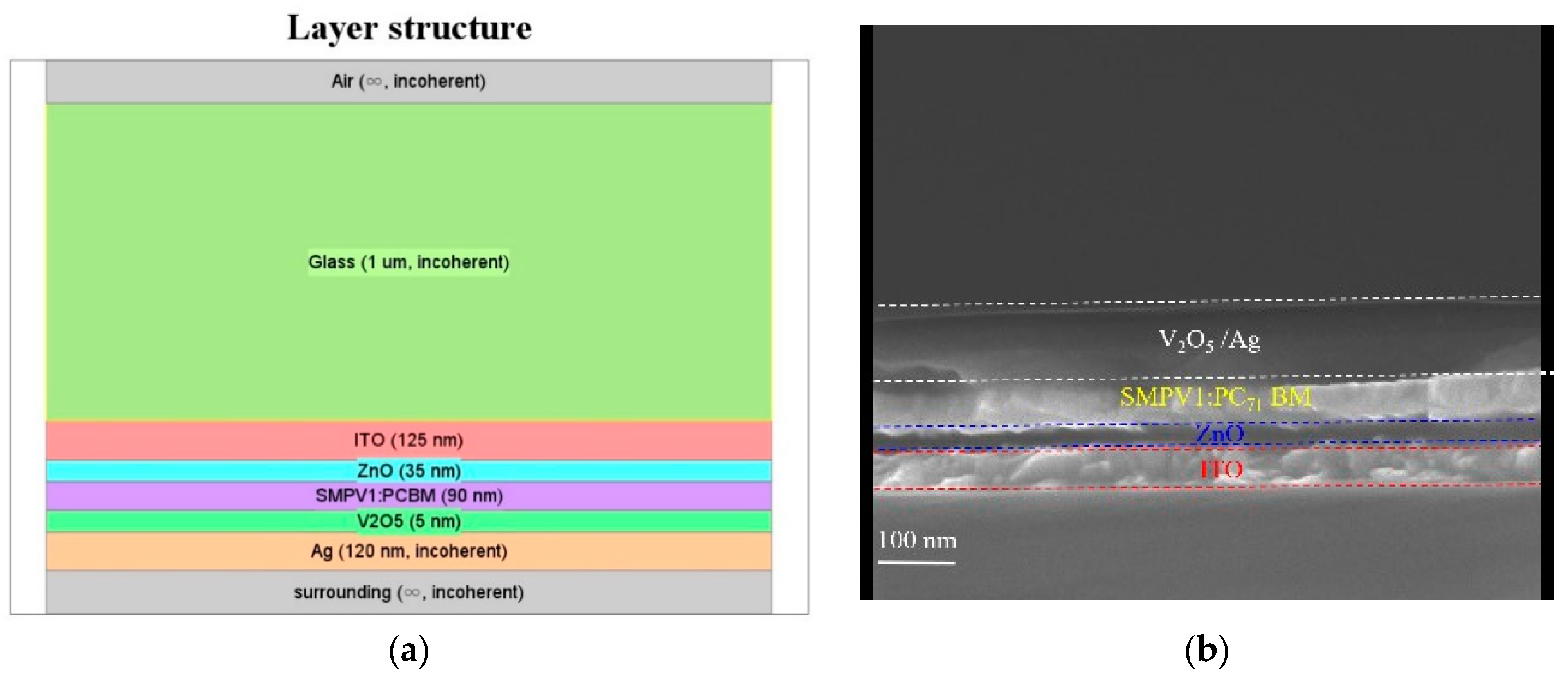
2. Materials and Methods

Figure 1a is a schematic diagram of the inverted nonhalogen small molecule solar cells consisting of layers of ITO/ZnO/SMPV1:PC71BM/V2O5 (5 nm)/Ag (120 nm). The ZnO seed layer (35 nm) was spin-coated from a 0.5-mol solution of zinc acetate in 2-Methoxyethanol (2MOE). Afterwards, a blend of SMPV1:PC71BM (1:0.8 by weight) mixed with a toluene solution was prepared on the ZnO seed layer by spin-coating. After spinning the active layer, the V2O5 layer and Ag electrode were deposited on top of the active layer under high vacuum. For comparison, another halogenated solvent-based sample was also prepared.
The electrical characteristics of the solar cells were measured in a glovebox at room temperature. To measure the efficiency of the solar cells, the devices were illuminated at 100 mW/cm2 from a 150 W Oriel solar simulator, using an air mass 1.5 global (AM 1.5G) filter to obtain the current density–voltage (J–V) curve. To make sure that the active layer matched with our optimized simulation result, SEM cross-sectional images were also taken, as provided in Figure 1b.

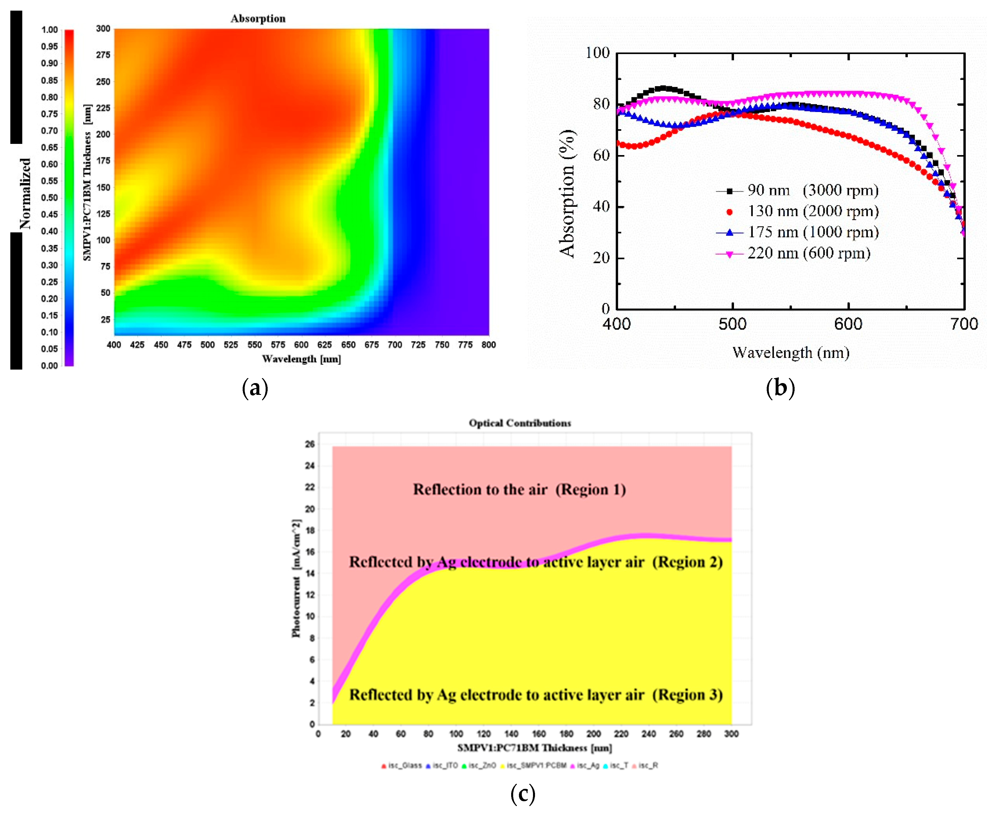
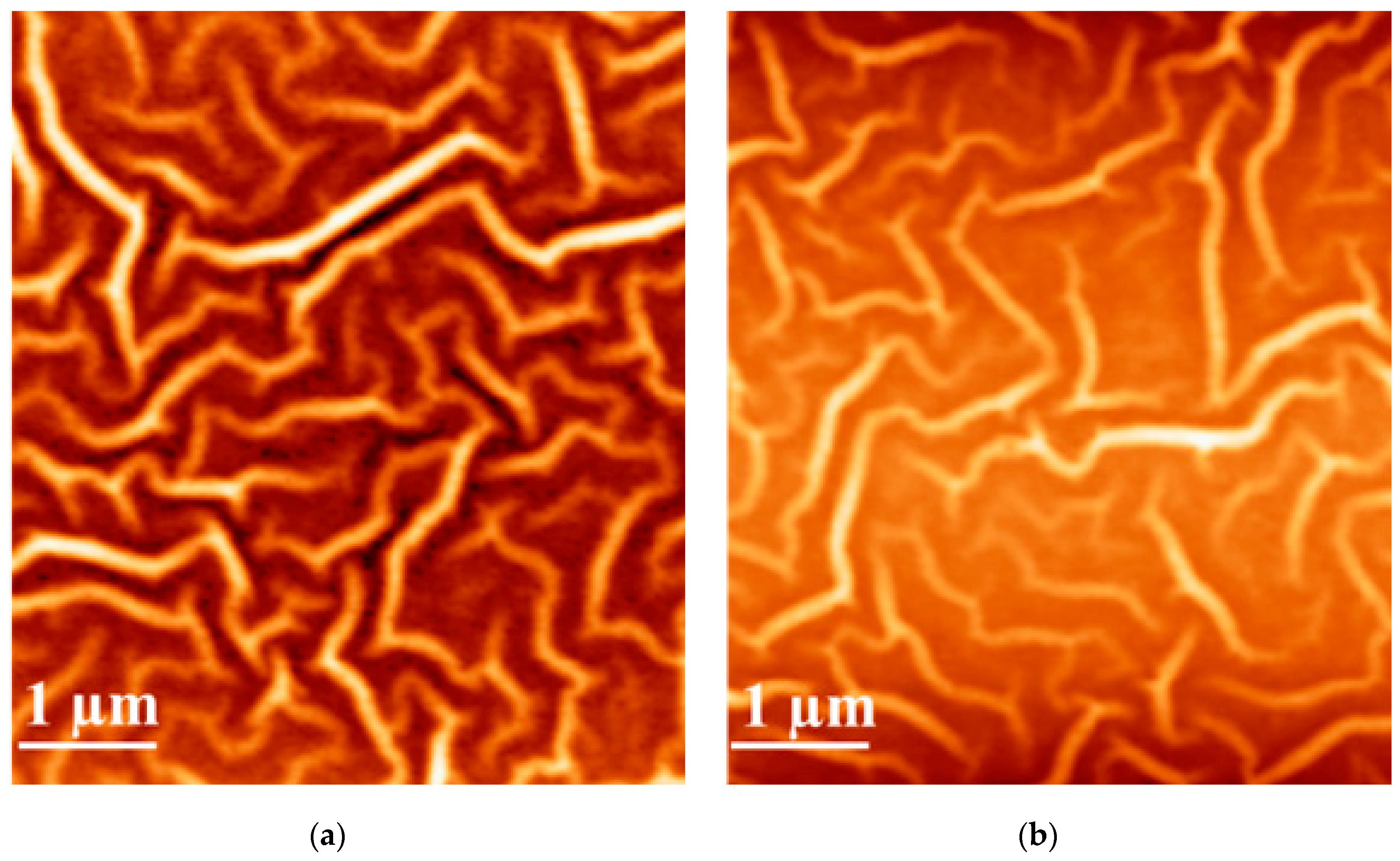
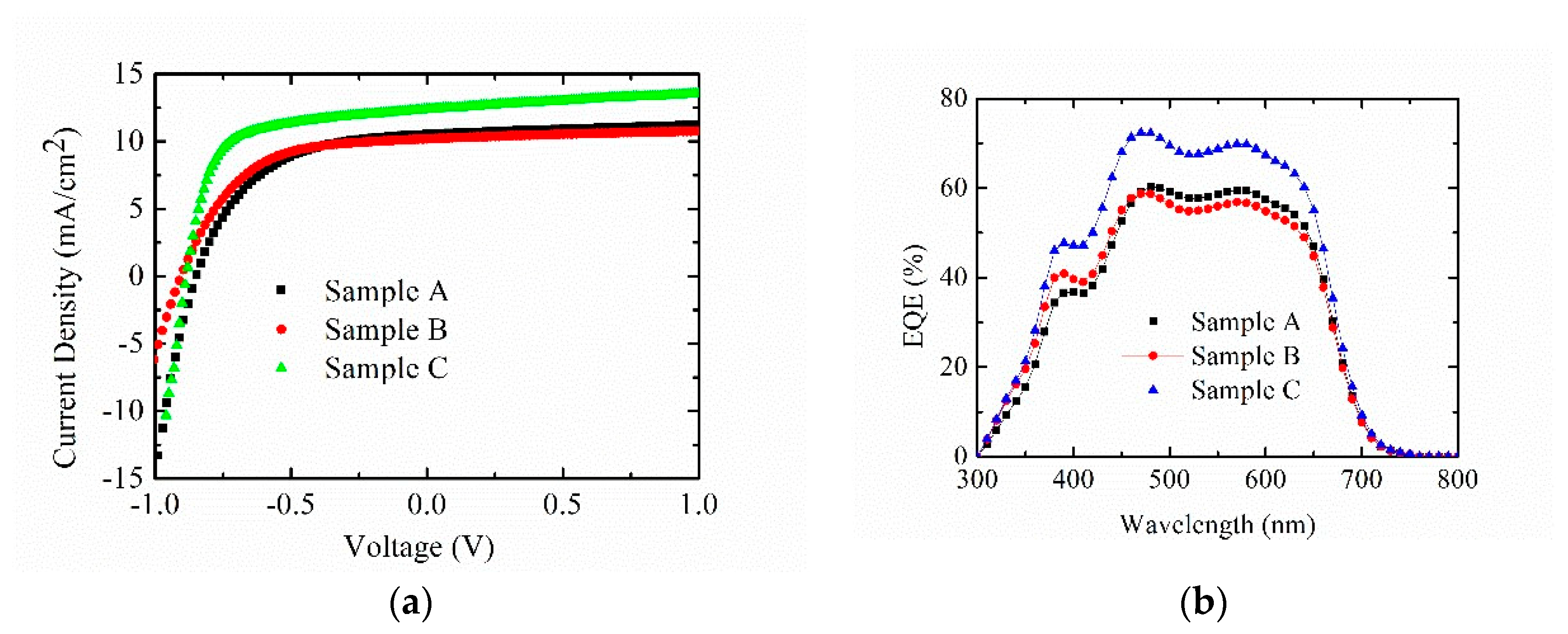
3. Results and Discussion

To understand the optical effects occurring in the inverted small molecule solar cell, the absorption spectrum of the devices was simulated for various thicknesses, as shown in Figure 2a. The varying device thicknesses resulted from different spin rates during the coating process, and was calculated using the commercial optical calculation software, SETFOS 5.0 (FLUXIM, 5.0, Switzerland). The obtained results are in good agreement with our previous research [15], calculated by the rigorous coupled wave analysis (RCWA) method. It is worth noting that the ripple in the spectrum simulated by RCWA is due to the interference phenomenon in the glass region. Therefore, in this study, to avoid the formation of ripples in the spectrum, the glass region was set to be in an incoherent state for the calculations. At a device thicknesses of 220 nm and 90 nm, a strong absorption in the active layer was observed, implying that either the device with 220 nm or that with 90 nm should exhibit the best performance. In the experimental verification, the device with a thickness of 90 nm was shown to perform better. This matches well with the previous reports [8,9,10,11]. Unlike OPVs, SM-OPVs generally possess shorter diffusion lengths, which dramatically limits the thickness of the active layer [16]. Therefore, the PCE of the SM-OPVs with the thickness of 220 nm were slightly compromised in comparison. Figure 2b shows the absorption spectra of the devices at various active layer thicknesses which resulted from different spin rates. The absorption spectra of the device with a thickness of 90 nm showed a strong signal at a wavelength of 450 nm. Moreover, the absorption spectra of the device with 220 nm thickness exhibited the highest signal throughout the visible wavelength. These results match well with the simulation, as shown in Figure 2a. Figure 2c shows the calculated photocurrent (mA/cm2) with various thicknesses. The internal quantum efficiency (IQE) was set to 100% initially. It was observed that the ideal photocurrent density could reach around 15.5 and 17.5 mA/cm2 with thicknesses of 90 and 220 nm, respectively. Moreover, in Figure 2c, there are three regions. Region 1 exhibits the reflection part of the incident light, which implies that almost 40.4% of the incident light was reflected and wasted at a thickness of 90 nm. Region 2 displays the optical enhancement originating from the light reflected by the Ag electrode. About 3.9% of the incident light was recycled by the Ag black electrode at a thickness of 90 nm. Region 3 shows the absorption part of the incident light. Almost 55.7% of the incident light was absorbed directly by the active layer at a thickness of 90 nm. To further accurately estimate the theoretical PCE of the various devices (Samples A, B, and C), the initial IQE was replaced and the new IQE spectra of the different devices were provided by measuring the external quantum efficiency (EQE) spectra, as shown in Figure 4b. The calculated PCEs are summarized in Table 1.
Table 1 summarizes the device performance of inverted SMPV1:PC71BM solar cells with various solvents and treatment conditions, such as current density Jsc, open circuit voltage Voc, fill factor (FF), and PCE. From the results, it may be seen that Sample A exhibited a lower FF of 52.6%, resulting in a lower PCE compared with Sample B. Despite similar Jsc, Sample B showed higher FF, which may be due to the varied surface morphology. In general, Jsc is mainly dependent on the absorption of the active layer, and the FF is dominated by the morphology. Therefore, it is vital to find a proper surface morphology that benefits the formation of the phase separation and bicontinuous interpenetrating connection in the active layer [10]. So far, SVA treatment is widely regarded as one of the best methods to effectively improve surface morphology, reduce carrier recombination, and improve device performance [17,18]. Therefore, in order to enhance the SM-OPV performance, our halogen-free devices further underwent a SVA process. By using SVA treatment, the FF of the device was enhanced from 56.4% to 66.8%. Consequently, the PCE of the device (Sample C) can be further improved to over 7%. It was noticed that the simulated results of PCE (Theoretical PCE) were very close to the practical results (PCE). By conducting the practical IQE of devices to the simulated model, the photocurrent density could be estimated accurately during the simulation. Therefore, the theoretical PCE could be improved as well.
In order to further verify that the SVA treatment in our work was related to the change of the morphology, which improved the surface condition at the interface, reduced the carrier recombination, we prepared films (ITO/ZnO/SMPV1:PC71BM ) with and without SVA treatment. Atomic force microscopy (AFM) top view images of the films are shown in Figure 3a,b. Due to the seed ZnO layer, the nano-ridge pattern of the active layer can be observed. It is worth noting that some defects in the center were compensated for after the SVA treatment, which implies that SVA treatment may benefit the interpenetrating network between the ZnO Electron-Transport Layer (ETL) and the active layer.
Figure 4a shows the J–V curves of samples A, B, and C. The thickness of the device (sample C) is determined by the SEM cross-sectional image, as shown in Figure 1b. The series resistance (Rs) and sheet resistance (Rsh) are calculated by the inverse of the curve gradients at V = 1 and V = 0 respectively [13]. From the results, Sample C can be observed to possess lower Rs compared to both samples A and B, implying that the SVA treatment is able to simultaneously prevent the leakage current and reduce the series resistance. The EQE of samples A, B, and C were also measured, and are shown in Figure 3b. According to the EQE spectra, the Jsc of the device can be calculated to be 9.91, 9.68, and 11.87 mA/cm2 respectively for samples A, B, and C [12]. The slight difference between the Jsc from the EQE and PCE results may be caused by the different measurement light source used, but both results exhibited similar trends nonetheless [15]

4. Conclusions

Halogen-free inverted SMPV1:PC71BM solar cells were fabricated and their performance was compared with halogenated solvent-based devices. The absorption spectra of the devices were simulated and verified experimentally. The PCE of halogen-free inverted SM-OPVs with the optimized active layer thickness of 90 nm reached over 5%. In order to further improve the performance of the device, the interface between the active layer and electrode of the optimized device was treated with the SVA process prior to the deposition of the electrode. By using SVA treatment, both the FF and Jsc could be improved. Hence, the PCE of the halogen-free inverted SMPV1:PC71BM solar cell can be improved, reaching 7.21%.

Author Contributions

Conceptualization, M.-Y.L.; investigation, M.-Y.L.; data curation, M.-Y.L. and C.-Y.L.; writing—original draft preparation, M.-Y.L.; Writing - review & editing, C.-Y.L. All authors have read and agreed to the published version of the manuscript.

Funding

This research was funded by Ministry of Science and Technology (Taiwan), No. MOST 108-2221-E-239-010 -.

Acknowledgments

This work was supported by the Ministry of Science and Technology of Taiwan and National United University.

Conflicts of Interest

The authors declare no conflict of interest.

References

  1. Dou, L.; You, J.; Yang, J.; Chen, C.C.; He, Y.; Murase, S.; Moriarty, T.; Emery, K.; Li, G.; Yang, Y. Tandem polymer solar cells featuring a spectrally matched low-bandgap polymer. Nat. Photonics 2012, 6, 180. [Google Scholar] [CrossRef]
  2. You, J.; Chen, C.C.; Dou, L.; Murase, S.; Duan, H.S.; Hawks, S.A.; Xu, T.; Son, H.J.; Yu, L.; Li, G.; et al. Metal Oxide Nanoparticles as an Electron-Transport Layer in High-Performance and Stable Inverted Polymer Solar Cells. Adv. Mater. 2012, 24, 5267. [Google Scholar] [CrossRef] [PubMed]
  3. Dou, L.; Gao, J.; Richard, E.; You, J.; Chen, C.C.; Cha, K.C.; He, Y.; Li, G.; Yang, Y. Systematic Investigation of Benzodithiophene- and Diketopyrrolopyrrole-Based Low-Bandgap Polymers Designed for Single Junction and Tandem Polymer Solar Cells. J. Am. Chem. Soc. 2012, 134, 10071. [Google Scholar] [CrossRef] [PubMed]
  4. Li, G.; Zhu, R.; Yang, Y. Polymer solar cells. Nat. Photonics 2012, 6, 153. [Google Scholar] [CrossRef]
  5. You, J.; Dou, L.; Yoshimura, K.; Kato, T.; Ohya, K.; Moriarty, T.; Emery, K.; Chen, C.; Gao, J.; Li, G.; et al. A polymer tandem solar cell with 10.6% power conversion efficiency. Nat. Commun. 2013, 4, 1446. [Google Scholar] [CrossRef] [PubMed] [Green Version]
  6. Chen, J.; Cui, C.; Li, Y.; Zhou, L.; Ou, Q.; Li, C.; Li, Y.; Tang, J. Single-Junction Polymer Solar Cells Exceeding 10% Power Conversion Efficiency. Adv. Mater. 2015, 27, 1035. [Google Scholar] [CrossRef] [PubMed]
  7. Gao, W.; Liu, T.; Ming, R.; Luo, Z.; Wu, K.; Zhang, L.; Xin, J.; Xie, D.; Zhang, G.; Ma, W.; et al. Near-Infrared Small Molecule Acceptor Enabled High-Performance Nonfullerene Polymer Solar Cells with Over 13% Efficiency. Adv. Funct. Mater. 2018, 28, 1803128. [Google Scholar] [CrossRef]
  8. Lin, M.Y.; Wu, S.H.; Hsiao, L.J.; Budiawan, W.; Chen, S.L.; Tu, W.C.; Lee, C.Y.; Chang, Y.C.; Chu, C.W. Well-aligned Vertically Oriented ZnO Nanorod Arrays and their Application in Inverted Small Molecule Solar Cells. J. Vis. Exp. 2018, 134, e56149. [Google Scholar] [CrossRef]
  9. Lin, M.Y.; Chen, T.J.; Xu, W.F.; Hsiao, L.J.; Budiawan, W.; Tu, W.C.; Chen, S.L.; Chu, C.W.; Wei, P.K. Fabrication of flexible indium tin oxide-free polymer solar cells with silver nanowire transparent electrode. Jpn. J. Appl. Phys. 2018, 57, 03DD01. [Google Scholar] [CrossRef]
  10. Liu, Y.; Chen, C.; Hong, Z.; Gao, J.; Yang, Y.M.; Zhou, H.; Dou, L.; Li, G.; Yang, Y. Solution-processed small-molecule solar cells: breaking the 10% power conversion efficiency. Sci. Rep. 2013, 3, 3356. [Google Scholar] [CrossRef] [PubMed] [Green Version]
  11. Farahat, M.E.; Tsao, C.S.; Huang, Y.C.; Chang, S.H.; Budiawan, W.; Wu, C.G.; Chu, C.W. Toward environmentally compatible molecular solar cells processed from halogen-free solvents. J. Mater. Chem. A 2016, 4, 7341. [Google Scholar] [CrossRef]
  12. Lin, M.Y.; Kang, Y.L.; Chen, Y.C.; Tsai, T.H.; Lin, S.C.; Huang, Y.H.; Chen, Y.J.; Lu, C.Y.; Lin, H.Y.; Wang, L.A.; et al. Plasmonic ITO-free polymer solar cell. Opt. Express 2014, 22, A438. [Google Scholar] [CrossRef] [PubMed]
  13. Lin, M.Y.; Lee, C.Y.; Shiu, S.C.; Wang, I.J.; Sun, J.Y.; Wu, W.H.; Lin, Y.H.; Huang, J.S.; Lin, C.F. Sol–gel processed CuOx thin film as an anode interlayer for inverted polymer solar cells. Org. Electron. 2010, 11, 1828. [Google Scholar] [CrossRef]
  14. Farahat, M.E.; Perumal, P.; Budiawan, W.; Chen, Y.F.; Lee, C.H.; Chu, C.W. Efficient molecular solar cells processed from green solvent mixtures. J. Mater. Chem. A 2017, 5, 571. [Google Scholar] [CrossRef]
  15. Lin, M.Y.; Su, V.C.; Chen, S.L. Partially green small molecule solar cells. In Proceedings of the 2019 26th International Workshop on Active-Matrix Flatpanel Displays and Devices (AM-FPD), Kyoto, Japan, 2–5 July 2019; IEEE: Piscataway, NJ, USA, 2019; Volume 26. [Google Scholar]
  16. Lin, M.Y.; Wu, S.H.; Hsiao, L.J.; Budiawan, W.; Boopathi, K.M.; Tu, W.C.; Chang, Y.C.; Chu, C.W. Enhance the light-harvesting capability of the ITO-free inverted small molecule solar cell by ZnO nanorods. Opt. Express 2016, 24, 17910. [Google Scholar] [CrossRef] [PubMed]
  17. Min, J.; Güldal, N.S.; Guo, J.; Fang, C.; Jiao, X.; Hu, H.; Heumüller, T.; Ade, H.; Brabec, C.J. Gaining further insight into the effects of thermal annealing and solvent vapor annealing on time morphological development and degradation in small molecule solar cells. J. Mater. Chem. A 2017, 5, 18101. [Google Scholar] [CrossRef]
  18. Tan, W.Y.; Gao, K.; Zhang, J.; Chen, L.; Wu, S.; Jiang, X.; Peng, X.; Hu, Q.; Liu, F.; Wu, H.; et al. Enhancing Performances of Solution-Processed Inverted Ternary Small-Molecule Organic Solar Cells: Manipulating the Host-Guest Donors and Acceptor Interaction. Sol. RRL 2017, 1, 1600003. [Google Scholar] [CrossRef]
Figure 1. Schematic diagrams of the nonhalogen small molecules solar cell structures. (b) SEM cross-sectional image of (a).
Crystals 10 00113 g001
Figure 2. (a) Simulated absorption spectra of the devices with the various thicknesses of active layer. (b) The absorption spectra of the devices with various active layer thicknesses. (c) Optical contribution by each layer.
Crystals 10 00113 g002
Figure 3. The AFM top view images of (a) without SVA treatment and (b) with SVA treatment.
Crystals 10 00113 g003
Figure 4. (a) The J–V curves of SM-OPVs with various solvents and treatment conditions. (b) The EQE spectra of sample A, sample B, and sample C.
Crystals 10 00113 g004
Table 1. Device performance of inverted SMPV1:PC71BM solar cells with various solvents and treatment conditions.
DeviceSolventSVA
Process
Voc
(V)
Jsc
(mA/cm2)
FFTheoretical PCE(%)PCE (%)
SampleACBX0.8510.5052.64.854.70
SampleBtolueneX0.8810.2156.45.395.07
SampleCtolueneO0.8712.4066.87.667.21

