Article

Enhanced Conversion Efficiency of a-Si:H Thin-Film Solar Cell Using ZnO Nanorods

1
Electrical Engineering Program C, Yuan-Ze University, 135 Yuan-Tung Road, Chung-Li 32003, Taiwan
2
Department of Electronic Engineering, Chang Gung University, 259 Wen-Hwa 1st Road, Kwei-Shan, Taoyuan 333, Taiwan
3
Department of Urology, Chang Gung Memorial Hospital, Linkou, No.5, Fuxing Street, Kwei-Shan, Taoyuan 333, Taiwan
4
School of Medicine, Chang Gung University, 259 Wen-Hwa 1st Road, Kwei-Shan, Taoyuan 333, Taiwan
*
Author to whom correspondence should be addressed.
Crystals 2020, 10(12), 1082; https://doi.org/10.3390/cryst10121082
Submission received: 14 October 2020 / Revised: 22 November 2020 / Accepted: 24 November 2020 / Published: 26 November 2020

Abstract

:
The surface reflectivity of a material will vary as light passes through interfaces with different refractive indices. Therefore, the optical loss and reflection of an optical-electronic component can be reduced by fabricating nanostructures on its surface. In the case of a solar cell, the presence of nanostructures can deliver many different advantages, such as decreasing the surface reflectivity, enhancing the light trapping, and increasing the efficiency of the carrier collection by providing a shorter diffusion distance for the photogenerated minority carriers. In this study, an approximately 50-nm thick seed layer was first prepared using spin coating. Zinc oxide nanorods (ZnO-NRs) were then grown using a chemical solution method (CSM). The ZnO-NRs were approximately 2 μm in height and 100 nm in diameter. After applying them to amorphous silicon (a-Si:H) solar cells, the short-circuit current density increased from 8.03 to 9.24 mA/cm2, and the photovoltaic conversion efficiency increased by 11.24%.

Graphical Abstract

1. Introduction

Solar cells made of a-Si:H films have long been the focus of attention. Compared to monocrystalline and polycrystalline silicon, a-Si:H has a relatively higher absorption coefficient. A merely 500-nm thick a-Si:H film can absorb sufficient solar light and be made into efficient solar cells. In comparison, the thickness of a solar cell made of monocrystalline or polycrystalline silicon should reach hundreds of microns. Therefore, an a-Si:H thin-film solar cell not only can effectively reduce the costs, but it also has the potential to be applied to flexible substrates owing to its thinner thickness. In addition, an a-Si:H thin-film solar cell has gradually stood out from various solar cells in recent years and created a global increase in investment. Once large-size glass substrate thin-film solar cells are introduced into the market, they will significantly accelerate the promotion and popularization of photovoltaic building integration, rooftop grid-connected power generation systems, and photovoltaic power plants. In addition, an a-Si:H thin-film solar cell exhibits only weak attenuation under high-temperature conditions, making it suitable for the construction of power plants in high-temperature and desert areas. At present, although the efficiency of a-Si:H thin-film solar cells has reached 10% [1], the high defect densities typically present in a-Si:H thin films limit the typical minority carrier diffusion lengths to 100 nm; consequently, a-Si:H solar cells are generally fabricated using even thinner a-Si:H layers, resulting in reduced absorption of incident solar radiation.
There are many approaches to increasing the light absorption, of which antireflective layers (ARLs) play an important role because they are capable of effectively reducing the Fresnel reflection loss at the interface between air and the top of the cell [2,3]. The common method of preparing an ARL is as follows: A single-layer or multi-layer ARL with a one-quarter wavelength of interest is used as silicon nitride and silicon oxide. However, single- or multi-layer ARLs have certain disadvantages such as the layer thickness control, material selection, material diffusion, a thermal expansion mismatch, and a small range of incident wavelengths and incident light angles [4]. In the past few years, it has been noted in different studies that a subwavelength grating (SWG) structure exhibits excellent broadband and omnidirectional antireflective optical properties, and the SWG of moth-eye pillars has thus begun to gradually replace traditional single- or multi-layer ARLs [5,6]. Fabrication processes involving electron beam lithography and dry etching have been widely used to fabricate various moth-eye structures in the past few years [7,8,9]. However, these fabrication processes are unsuitable for the mass production of nanostructures on large-area solar cells because the process-induced surface recombination defects reduce the performance of the device. Therefore, many scholars have developed bottom-up growth approaches to fabricate the nanostructures [10,11,12].
ZnO is a wide-direct band gap material for 3.37 eV semiconductors and has been used in several ZnO structures as ARLs [13,14], including nanoflowers [15,16], nanorods [17,18], nanotrees [19,20], and nanosheets [21,22]. However, the corresponding fabrication cost is high. The growth of ZnO nanostructures using the chemical solution method (CSM) approach, by contrast, carries significant potential. Compared to the traditional growth methods of ZnO nanostructures, the CSM approach has the advantages of low-temperature growth and low cost, in addition to its low technical threshold and large production capacity. Therefore, this study will fabricate zinc oxide nanorods (ZnO-NRs) on an a-Si:H thin-film solar cell using a CSM to improve the photovoltaic conversion efficiency.
According to the previous literature, D.N. Papadimitriou used electrochemical deposition (ECD) techniques to deposit Al:ZnO-NR as an antireflective layer on the surface of Cu(In,Ga)Se2 solar cells. This structure effectively reduced the weighted global reflectance of devices by approximately 5% and improved the photoelectric conversion efficiency by approximately 5% [13]. Xuegong Yu’s team used the chemical solution method to grow ZnO nanowires with different lengths on the surface of polycrystalline silicon solar cells, thereby reducing the reflectivity of the device and improving the photoelectric conversion efficiency. Using this method, the photoelectric conversion efficiency was effectively improved by approximately 3% [14]. In this study, CSM was used to grow ZnO nanorods on the surface of a-Si:H thin-film solar cell, which effectively improved the photoelectric conversion efficiency by approximately 11.24%.

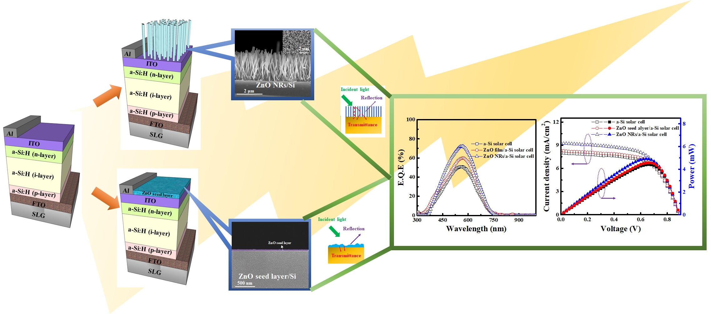
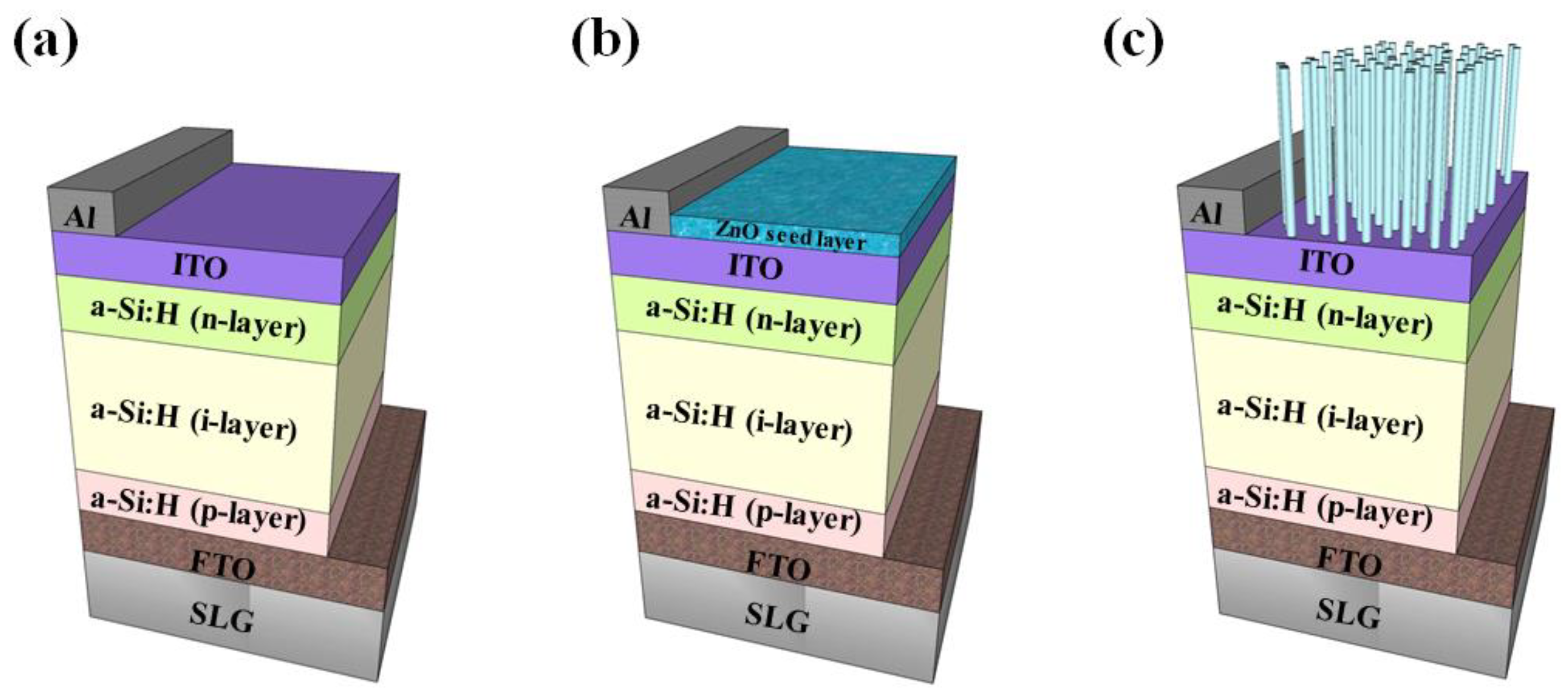
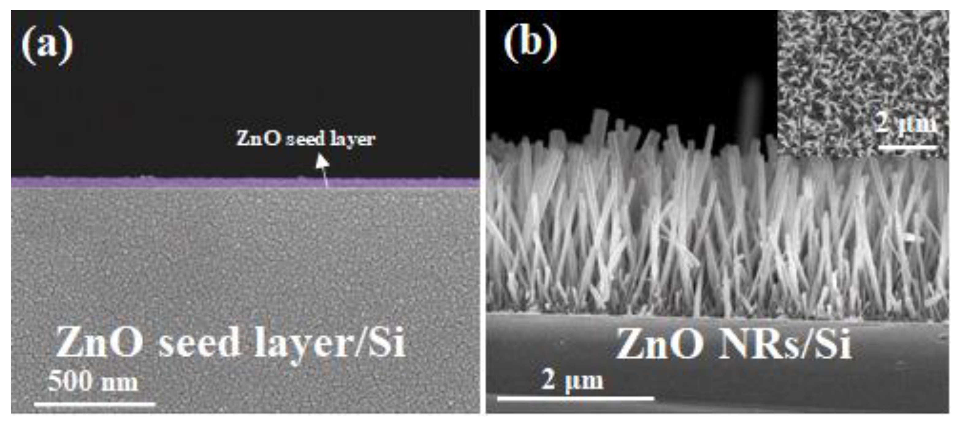
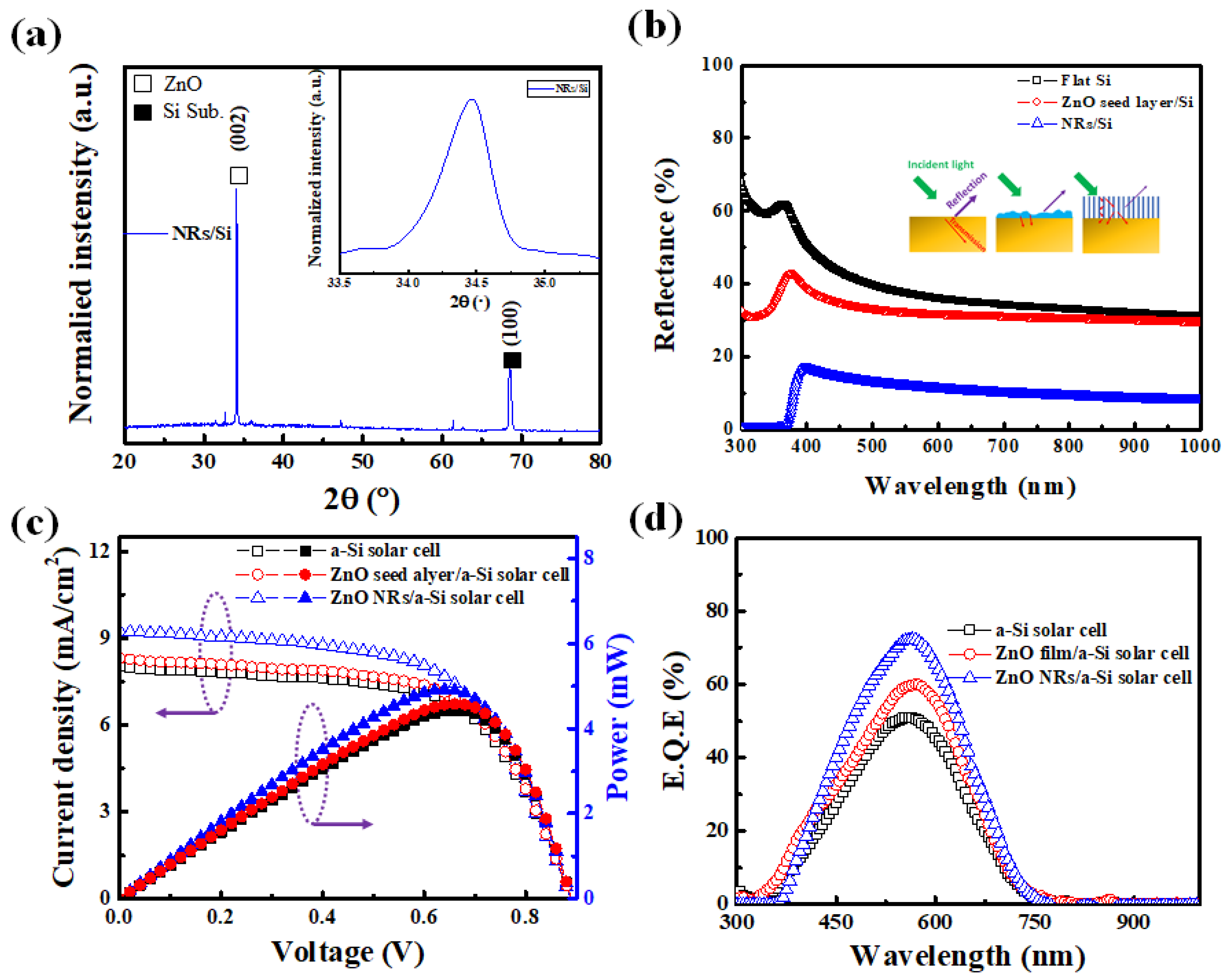
2. Materials and Methods

Before the growth process, the Si substrates were coated with a ZnO nanoparticle layer using a sol-gel preparation as the seeding layer. The crystalline seed layer was prepared in an environment of up to 140 °C, and was then annealed in an atmospheric environment. Next, the seed layer was placed in a chemical solution of 0.03 M hexamethylenetetramine mixed with 0.03 M zinc nitrate hexahydrate, and it was grown at 90 °C for 18 h to yield ZnO-NRs. The corresponding reaction formulas are as follows:
C 6 H 12 N 4 + 6 H 2 O 6 HCHO + 4 NH 3
NH 3 + H 2 O NH 4 + + OH
Zn 2 + + 2 OH Zn ( OH ) 2
Zn ( OH ) 2 ZnO + H 2 O
The reflectivity of the ZnO-NRs grown on the Si substrate and the ZnO seed layer was then measured using a UV-vis spectrometer. The entire fabrication process was then introduced to an a-Si:H film solar cell. The a-Si:H thin-film solar cells used in this study, as shown in Figure 1, are made of a-Si:H films applied at 140 °C with a very high frequency plasma enhanced chemical vapor deposition (VHF-PECVD) system operating at 40 MHz with a power density of 83 mW/cm2. On a SnO2:F substrate, doped layers with a thickness of 12 nm (p-layer) or 20 nm (n-layer) were synthesized using VHF-PECVD with an admixture of 10% B2H6 (p-layer) or 3% PH3 (n-layer), respectively. After that, a 150-nm thick layer of In2O3:Sn (ITO) was deposited as a transparent conductive layer through DC-sputtering. Al was also deposited as an electrode using DC-sputtering.

3. Results

Figure 2a,b shows the cross-sectional scanning electron microscope (SEM) views of the ZnO seed layer and the ZnO-NRs, respectively. It can be seen from Figure 2a that the thickness of the ZnO seed layer is approximately 50 nm. From Figure 2b, it can be seen that the ZnO-NRs are approximately 2 µm in length. In addition, ZnO-NRs demonstrated an average diameter of 100 nm, shown in top view illustration in Figure 2.
Figure 3a shows an X-ray diffractometer (XRD) diagram of the ZnO-NRs grown on a Si substrate. Two distinct signals can be observed, which correspond to the ZnO (002) and Si (100) planes, respectively. Other compounds were not observed in XRD analysis. The full width at half maximum (FWHM) calculated from the XRD spectra is in indication of crystallinity, and our experimental results show that the value of FWHM (~0.35°) is comparable to that reported in previous literature [23]. Generally, a lattice mismatch will exist between the different materials due to the difference in lattice constants of the constituent compounds. It is thought that strain effects can induce material distortion and microfracture, leading to device failure. Thus, in our study, the low-temperature buffer layer is introduced to accommodate lattice strain leading to the growth of almost strain-free ZnO nanorods. Our XRD results were consistent with JCPDS 36-1451. Therefore, it is speculated that the ZnO nanorods growing on the surface of a-Si:H solar cells showed a mismatch-strain-free characteristic. Furthermore, as seen in other literatures, nanostructures could still be used normally on devices after they pass the reliability and stability tests [24,25,26].
Figure 3b gives the reflectivity values of the Si substrate, the ZnO seed layer/Si, and the ZnO-NRs/Si. Within the wavelength range of 300–1000 nm, the average reflectivity values of the Si substrate, the ZnO seed layer/Si, and the ZnO-NRs/Si are 39.05%, 32.05%, and 9.61%, respectively. The slight reduction in reflectivity of the ZnO seed layer/Si might be attributed to the uneven surface topography. The main reason for the reduced reflectivity of ZnO-NRs/Si is the subwavelength structures produce a gradient refractive index profile between the material (refractive index > 1) and air (refractive index = 1) to reduce the Fresnel reflection and provide a more effective thermal stability and durability than surface coatings as only one material is used. Furthermore, the subwavelength structures are smaller than the wavelength of light and trap light through the diffraction of incident light in the nanostructure [27,28,29]. Figure 3c shows the current density–voltage (J-V) curves, which compare the differences among one bare a-Si:H thin-film solar cell, a cell with a ZnO seed layer coated on the ITO layer, and a cell with ZnO-NRs. The parameter arrangement from the experimental measurement results is listed in Table 1.
The conversion efficiencies (η) of the bare solar cell and cells with a ZnO seed layer and ZnO-NRs are 4.42%, 4.57%, and 4.98%, respectively. The open-circuit voltage (Voc) is approximately 885 mV; the fill factor (F.F.) is 60%; and the short circuit current (Jsc) values are 8.02, 8.3, and 9.24 mA/cm2, respectively. Therefore, the increase in the efficiency of the a-Si:H thin-film solar cell mainly resulted from the increase in Jsc. The maximum increase in photocurrent enhancement factor (EFjsc) is 15.15%, as calculated by the following formula:
EF jsc = Δ J sc J sc = J sc ( with   ARL ) J sc ( without   ARL ) J sc ( without   ARL )
Figure 3d shows the results of the external quantum efficiency (EQE) measurements, which also proved the increases in η as a result of fabricating the ZnO seed layer and the ZnO-NRs on the ITO layer. Compared with the bare a-Si:H thin-film solar cell, the cells with the ZnO seed layer and ZnO-NRs exhibited enhanced photo-responses within a wavelength range of approximately 400–750 nm. Compared with a bare a-Si:H thin-film solar cell, the ZnO-NRs exhibited a stronger antireflective property, which resulted in an improved Jsc for the a-Si:H thin-film solar cell with ZnO-NRs.

4. Conclusions

In summary, the reflectivity of the a-Si:H thin-film solar cell was reduced significantly by fabricating the ZnO seed layer and the ZnO-NRs on the ITO layer. Results showed that a ZnO seed layer was deposited on the surface of an a-Si:H thin-film solar cell as the ARL and the current density increased from the initial 8.02 to 8.3 mA/cm2. The photoelectric conversion efficiency was improved by approximately 3.39%. ZnO-NRs grown on the surface of an a-Si:H thin-film solar cell was used as ARL and the current density increased from the initial 8.02 to 9.24 mA/cm2. The conversion efficiency of the solar cell increased from 4.42% to 4.98%. This study has shown that ZnO-NRs can be used as an ARL for an a-Si:H thin-film solar cell, thereby providing a suitable alternative to other solar cells.

Author Contributions

Conceptualization: F.-I.L., and S.-Y.K.; methodology, J.-F.Y., and Y.-C.H.; validation, F.-I.L., S.-Y.K. and J.-F.Y.; formal analysis, Y.-C.H.; investigation, J.-F.Y. and Y.-C.H.; resources, F.-I.L., S.-Y.K. and Y.-C.H.; data curation, J.-F.Y.; writing—original draft preparation, J.-F.Y.; writing—review and editing, S.-Y.K.; supervision, S.-Y.K.; project administration, F.-I.L.; funding acquisition, F.-I.L., S.-Y.K. and Y.-C.H. All authors have read and agreed to the published version of the manuscript.

Funding

This research was funded by Chang Gung Memorial Hospital (BMRP 956) and Ministry of Science and Technology (MOST 108-2112-M-182-001-MY3, MOST 107-2221-E-155-055-MY3).

Acknowledgments

This research was supported by the Green Technology Research Center of Chang Gung University.

Conflicts of Interest

The authors declare no conflict of interest. The funders had no role in the design of the study; in the collection, analyses, or interpretation of data; in the writing of the manuscript; or in the decision to publish the results.

References

  1. Matsui, T.; Maejima, K.; Bidiville, A.; Sai, H.; Koida, T.; Suezaki, T.; Matsumoto, M.; Saito, K.; Yoshida, I.; Kondo, M. High-efficiency thin-film silicon solar cells realized by integrating stable a-Si:H absorbers into improved device design. Jpn. J. Appl. Phys. 2015, 54, 08KB10. [Google Scholar] [CrossRef]
  2. Li, D.; Liu, Z.; Wang, Y.; Shan, Y.; Huang, F. Efficiency Enhancement of Cu(In,Ga)Se2 Solar Cells by Applying SiO2-PEG/PVP Antireflection Coatings. J. Mater. Sci. Technol. 2015, 31, 229–234. [Google Scholar] [CrossRef] [Green Version]
  3. Chang, Y.-A.; Li, Z.-Y.; Kuo, H.-C.; Lu, T.-C.; Yang, S.-F.; Lai, L.-W.; Lai, L.-H.; Wang, S.-C. Efficiency improvement of single-junction InGaP solar cells fabricated by a novel micro-hole array surface texture process. Semicond. Sci. Technol. 2009, 24, 085007. [Google Scholar] [CrossRef] [Green Version]
  4. Baek, S.-H.; Kim, S.-B.; Shin, J.-K.; Kim, J.-H. Preparation of hybrid silicon wire and planar solar cells having ZnO antireflection coating by all-solution processes. Sol. Energy Mater. Sol. Cells 2012, 96, 251–256. [Google Scholar] [CrossRef]
  5. Shao, T.; Tang, F.; Sun, L.; Ye, X.; He, J.; Yang, L.; Zheng, W. Fabrication of Antireflective Nanostructures on a Transmission Grating Surface Using a One-Step Self-Masking Method. Nanomaterials 2019, 9, 180. [Google Scholar] [CrossRef] [Green Version]
  6. Rouzo, J.-L.; Brückner, J.-B.; Ferchichi, A.; Gourgon, C.; Berginc, G.; Escoubas, L. Optical properties of antireflective flat or rough patterned topped silicon cones gratings. Adv. Device Mater. 2015, 1, 23–26. [Google Scholar] [CrossRef]
  7. Ducros, C.; Brodu, A.; Lorin, G.; Emieux, F.; Pereira, A. Optical performances of antireflective moth-eye structures. Comparison with standard vacuum antireflection coatings for application to outdoor lighting LEDs. Surf. Coat. Technol. 2019, 379, 125044. [Google Scholar] [CrossRef]
  8. Liu, Y.; Soltani, M.; Dey, R.-K.; Cui, B.; Lee, R.; Podmore, H. Moth-eye antireflection nanostructure on glass for CubeSats. J. Vac. Sci. Technol. B 2018, 36, 06JG01. [Google Scholar] [CrossRef]
  9. Lotz, M.-R.; Petersen, C.-R.; Markos, C.; Bang, O.; Jakobsen, M.-H.; Taboryski, R. Direct nanoimprinting of moth-eye structures in chalcogenide glass for broadband antireflection in the mid-infrared. Optica 2018, 5, 557–563. [Google Scholar] [CrossRef]
  10. Ren, X.; Sangle, A.; Zhang, S.; Yuan, S.; Zhao, Y.; Shi, L.; Hoye, R.-L.-Z.; Cho, S.; Li, D.; MacManus-Driscoll, J.-L. Photoelectrochemical water splitting strongly enhanced in fast-grown ZnO nanotree and nanocluster structures. J. Mater. Chem. A 2016, 4, 10203–10211. [Google Scholar] [CrossRef] [Green Version]
  11. Son, D.-Y.; Im, J.-H.; Kim, H.-S.; Park, N.-G. 11% Efficient Perovskite Solar Cell Based on ZnO Nanorods: An Effective Charge Collection System. J. Phys. Chem. C 2014, 118, 16567–16573. [Google Scholar] [CrossRef]
  12. Jin, D.; Gu, X.; Yu, X.; Ding, G.; Zhu, H.; Yao, K. Hydrothermal synthesis and characterization of hexagonal Mg(OH)2 nano-flake as a flame retardant. Mater. Chem. Phys. 2008, 112, 962–965. [Google Scholar] [CrossRef]
  13. Papadimitriou, D.-N. Structural, optical, electrical properties, and strain/stress of electrochemically deposited highly doped ZnO layers and nanostructured ZnO antireflective coatings for cost-effective photovoltaic device technology. Thin Solid Films 2016, 605, 215–231. [Google Scholar] [CrossRef]
  14. Yu, X.; Dong, W.; Dong, L.; Li, G.; Yang, D. Efficiency improvement of silicon solar cells enabled by ZnO nanowhisker array coating. Nanoscale Res. Lett. 2012, 7, 306. [Google Scholar] [CrossRef] [PubMed] [Green Version]
  15. Rupa, E.-J.; Kaliraj, L.; Abid, S.; Yang, D.-C.; Jung, S.-K. Synthesis of a Zinc Oxide Nanoflower Photocatalyst from Sea Buckthorn Fruit for Degradation of Industrial Dyes in Wastewater Treatment. Nanomaterials 2019, 9, 1692. [Google Scholar] [CrossRef] [Green Version]
  16. Upadhyay, A.; Yang, H.; Zaman, B.; Zhang, L.; Wu, Y.; Wang, J.; Zhao, J.; Liao, C.; Han, Q. ZnO Nanoflower-Based NanoPCR as an Efficient Diagnostic Tool for Quick Diagnosis of Canine Vector-Borne Pathogens. Pathogens 2020, 9, 122. [Google Scholar] [CrossRef] [Green Version]
  17. Bhushan, B.; Murty, B.-S.; Mondal, K. A new approach for synthesis of ZnO nanorod flowerets and subsequentpure free-standing ZnO nanorods. Adv. Powder Technol. 2019, 30, 30–41. [Google Scholar] [CrossRef]
  18. Li, X.; Chen, X.; Yi, Z.; Zhou, Z.; Tang, Y.; Yi, Y. Fabriction of ZnO Nanorods with Strong UV Absorption and Different Hydrophobicity on Foamed Nickel under Different Hydrothermal Conditions. Micromachines 2019, 10, 164. [Google Scholar] [CrossRef] [Green Version]
  19. Zhao, F.; Zheng, J.-G.; Yang, X.; Li, X.; Wang, J.; Zhao, F.; Wong, K.-S.; Liang, C.; Wu, M. Complex ZnO nanotree arrays with tunable top, stem and branch structures. Nanoscale 2010, 2, 1674–1683. [Google Scholar] [CrossRef]
  20. Zhao, F.; Li, X.; Zheng, J.-G.; Yang, X.; Zhao, F.; Wong, K.-S.; Wang, J.; Lin, W.; Wu, M.; Su, Q. ZnO Pine-Nanotree Arrays Grown from Facile Metal Chemical Corrosion and Oxidation. Chem. Mater. 2008, 20, 1197–1199. [Google Scholar] [CrossRef]
  21. Iqbal, T.; Khan, M.-A.; Mahmood, H. Facile synthesis of ZnO nanosheets: Structural, antibacterial and photocatalytic studies. Mater. Lett. 2018, 224, 59–63. [Google Scholar] [CrossRef]
  22. Dahiya, A.-S.; Sporea, R.-A.; Poulin-Vittrant, G.; Alquier, D. Stability evaluation of ZnO nanosheet based source-gated transistors. Sci. Rep. 2019, 9, 2979. [Google Scholar] [CrossRef] [PubMed] [Green Version]
  23. Shabannia, R. Vertically aligned ZnO nanorods on porous silicon substrates: Effect of growth time. Prog. Nat. Sci. Mater. Int. 2015, 25, 95–100. [Google Scholar] [CrossRef] [Green Version]
  24. Yao, I.-C.; Lin, P.; Tseng, T.-Y. Field Emission Properties and Reliability of ZnO Nanorod, Nanopagoda, and Nanotip Current Emitters. IEEE Trans. Nanotechnol. 2012, 11, 746–750. [Google Scholar] [CrossRef]
  25. Ye, Z.; Ji, X.; Zhang, Q. Enhanced field emission properties of ZnO nanorods by surface modification. RSC Adv. 2015, 5, 78502–78507. [Google Scholar] [CrossRef]
  26. Lai, F.-I.; Yang, J.-F.; Liao, W.-X.; Kuo, S.-Y. Enhanced omnidirectional and weatherability of Cu2ZnSnSe4 solar cells with ZnO functional nanorod arrays. Sci. Rep. 2017, 7, 14927. [Google Scholar] [CrossRef] [Green Version]
  27. Lalanne, P.; Morris, G.-M. Antireflection behavior of silicon subwavelength periodic structures for visible light. Nanotechnology 1997, 8, 53–56. [Google Scholar] [CrossRef]
  28. Chiu, M.-Y.; Chang, C.-H.; Tsai, M.-A.; Chang, F.-Y.; Yu, P. Improved optical transmission and current matching of a triple-junction solar cell utilizing sub-wavelength structures. Opt. Express 2010, 18, A308–A313. [Google Scholar] [CrossRef]
  29. Leem, J.-W.; Joo, D.-H.; Yu, J.-S. Biomimetic parabola-shaped AZO subwavelength grating structures for efficient antireflection of Si-based solar cells. Sol. Energy Mater. Sol. Cells 2011, 95, 2221–2227. [Google Scholar] [CrossRef]
Figure 1. Schematic plot of the fabricated a-Si:H thin-film solar cell: (a) bare, (b) with a ZnO seed layer, and (c) with ZnO-NRs.
Crystals 10 01082 g001
Figure 2. (a) Seed layer and (b) SEM cross-sectional view of ZnO-NRs; the illustration shows a top-view SEM of the ZnO-NRs.
Crystals 10 01082 g002
Figure 3. (a) XRD diagram of the ZnO-NRs, with the illustration showing an enlarged view of the plane (002); (b) reflectivity plot after depositing the ZnO seed layer and growing the ZnO-NRs on the Si substrate, (c) J–V curves of different antireflective layers (ARLs) growing on the a-Si:H thin-film solar cells under AM1.5 G (100 mW/cm2), and (d) EQE spectrum of different ARLs growing on a-Si:H thin-film solar cells.
Crystals 10 01082 g003
Table 1. Photovoltaic parameters of different antireflective layer film with a-Si:H thin-film solar cells.
SampleEfficiency (%)Voc (mV)Jsc (mA/cm2)F.F.
a-Si:H solar cell4.428858.0262.27
ZnO seed layer/a-Si:H solar cell4.578858.362.21
ZnO NRs/a-Si:H solar cell4.988859.2460.9
Publisher’s Note: MDPI stays neutral with regard to jurisdictional claims in published maps and institutional affiliations.

