Review

Metal Chalcogenides on Silicon Photocathodes for Efficient Water Splitting: A Mini Overview

Department of Energy Science, Sungkyunkwan University, Suwon 16419, Korea
*
Authors to whom correspondence should be addressed.
These authors contributed equally to this work.
Catalysts 2019, 9(2), 149; https://doi.org/10.3390/catal9020149
Submission received: 29 November 2018 / Revised: 2 January 2019 / Accepted: 8 January 2019 / Published: 2 February 2019
(This article belongs to the Special Issue Semiconductor Catalysis)

Abstract

:
In the photoelectrochemical (PEC) water splitting (WS) reactions, a photon is absorbed by a semiconductor, generating electron-hole pairs which are transferred across the semiconductor/electrolyte interface to reduce or oxidize water into oxygen or hydrogen. Catalytic junctions are commonly combined with semiconductor absorbers, providing electrochemically active sites for charge transfer across the interface and increasing the surface band bending to improve the PEC performance. In this review, we focus on transition metal (di)chalcogenide [TM(D)C] catalysts in conjunction with silicon photoelectrode as Earth-abundant materials systems. Surprisingly, there is a limited number of reports in Si/TM(D)C for PEC WS in the literature. We provide almost a complete survey on both layered TMDC and non-layered transition metal dichalcogenides (TMC) co-catalysts on Si photoelectrodes, mainly photocathodes. The mechanisms of the photovoltaic power conversion of silicon devices are summarized with emphasis on the exact role of catalysts. Diverse approaches to the improved PEC performance and the proposed synergetic functions of catalysts on the underlying Si are reviewed. Atomic layer deposition of TM(D)C materials as a new methodology for directly growing them and its implication for low-temperature growth on defect chemistry are featured. The multi-phase TM(D)C overlayers on Si and the operation principles are highlighted. Finally, challenges and directions regarding future research for achieving the theoretical PEC performance of Si-based photoelectrodes are provided.

1. Introduction

Photoelectrochemical (PEC) water splitting (WS) utilizes sunlight to oxidize or reduce water into oxygen and hydrogen. It is a promising concept for clean fuel production in that no energy cost is required when compared with the electrocatalytic (EC) counterparts. The conversion of solar power to feasible gas fuels (hydrogen and oxygen) out of water requires semiconductors as absorbers having suitable band gaps whose position straddles the water redox potential (E0 = 1.229 eV) along with sustainable, Earth-abundant and efficient catalytic overlayers. Silicon (Si) is one of the most intensively studied semiconductors in the field of PEC WS as a light absorber thanks to its suitable band gap (1.12 eV), Earth-abundance and validity in existing electronics industries. The maximum photovoltage (Vph) of Si is in the range of 0.45 to 0.5 V, with a photocurrent density (Jph) of approximately 44 mAcm−2 [1]. However, Si itself suffers from (photo)corrosion in electrolyte solutions. The surface states of Si induce surface recombination between the Si/electrolyte interfaces and significantly reduce the surface energetics and kinetics leading to decreases of both Vph and Jph. This is the result of Fermi-level pinning (FLP) and recombination at the electrode/electrolyte interface, which is already prevalent in the metal-semiconductor (MS) junction in solid-state physics [2]. Therefore, the surface modification strategy of applying co-catalysts is necessary, and significant progress has been made in designing efficient photoelectrodes, primarily using the high work function noble metals (platinum (Pt) or Pt-group metals), which have shown the best catalytic activities for hydrogen production to date. To overcome the cost limitation for large-scale production, searching for Earth-abundant and efficient alternatives, such as high work function metals, chalcogenides, nitrides, phosphides, carbides, and metal oxides has received great interest in the field of PEC WS [3,4]. Moreover, the roles of the catalytic effects such as increasing Vph and efficient charge transfer, and the plausible mechanisms have been studied recently [5,6].
With these efforts, the tandem-structured PEC cells with co-catalysts have been investigated for the purpose of unbiased and unassisted PEC WS. A tandem PEC cell consists of the top cell that absorbs short wavelength light and the bottom cell that absorbs light of a long wavelength that was transmitted after the top one. The two-stage light absorption/conversion is an important strategy for better photovoltage and efficient photoconversion. The Lewis group calculated the optimal band gap of the light absorber and the theoretical solar-to-hydrogen limits for constructing the tandem PEC cell [7]. Si has long been used as a photocathode with variously modified oxide photoanodes to construct PEC-PEC tandem cells for improving the solar-to-hydrogen efficiency. Abdi et al. reported an excellent STH of 5% through the cobalt phosphate layers on the tandem cell configuration of W-doped BiVO4 photoanode and Si photocathode [8]. Nonetheless, the research activities on the tandem structures with modifying Si remain in their infancy [9]. Therefore, it is highly desired to study the improved cathodic reactions by conjunction with various co-catalytic materials.
Transition metal (di)chalcogenide [TM(D)C] materials are promising due to the unique physical, optical and electronic properties [10,11]. Many of the TM(D)Cs are layered materials, consisting of honeycomb transition metal (M) atoms sandwiched by chalcogenide (X) layers. For example, MoS2 is composed of a triple layer of strongly covalent bonding S-Mo-S and weak van der Waals (vdW) bonding S-S. Similarly, the ordered quintuple layers, such as Te1-Bi-Te2-Bi-Te1 can also constitute a unique layered structure, where the Te1-Te1 bond is of the van der Waals’ type (i.e., M2X3 type). With the unique bonding properties of TM(D)C that comprise covalent bonding between M-X and vdW interaction between X-X, TM(D)C shows characteristic charge transport and phonon propagation properties. These bonding characters, consequentially, exhibit strong anisotropy which can be utilized in many different applications. They have been applied in the studies from solid lubricant to thermoelectric materials [12,13]. In particular, relatively wider vdW gaps than ionic species could be promising as battery materials [14]. TM(D)C materials possessing intrinsic semiconducting properties can be transformed into metal by either distorting the X structures or intercalating ions into the vdW gap. The layered structures can be easily delaminated into very thin layers by exfoliation and can be used as a charge transport layer of solar cells having excellent mobility values [15]. Moreover, the dangling bonds where the catalytic activity is expected to be high are rare on the basal plane, and thus, more stable against the electrochemical reactions in the electrolyte [16]. The exposed edge sites are proved to be responsible for fast charge transfer kinetics at the electrode/electrolyte interface. Therefore, MoS2 has been studied as one of the most efficient catalysts for EC [17]. TM(D)C materials combined to semiconductor absorbers including Si have been reported for improved PEC performance.
In this review, we introduce the basic mechanisms of Si-based photoelectrodes, focusing mostly on photocathodes with a brief look at the progress achieved so far. Si photocathodes combined with TM(D)C materials will be the main focus of this review. Various synthesis routes of Si/TM(D)C structures are also summarized, and the atomic layer deposition (ALD) technique is highlighted as the direct growth method at low temperatures. The implications of low-temperature formation on the defect chemistry of chalcogenides are featured. Finally, we highlight the recent reports on the multi-/mixed-phase TM(D)C layers on Si for application in PEC WS. The related energetic and kinematic mechanisms are also discussed for the design of high-performance photoelectrodes.

2. Photo-Assisted Electrochemical Water Splitting

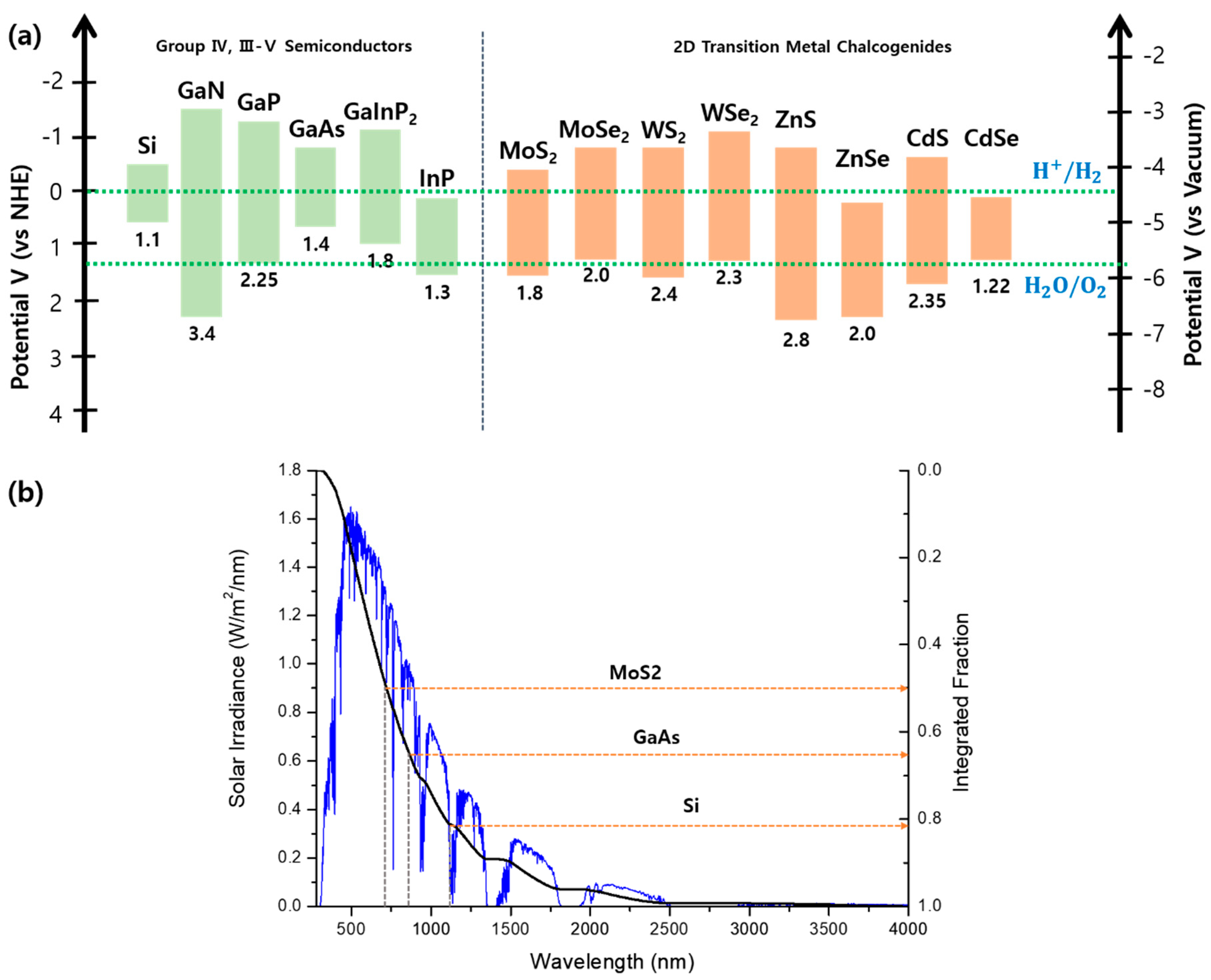
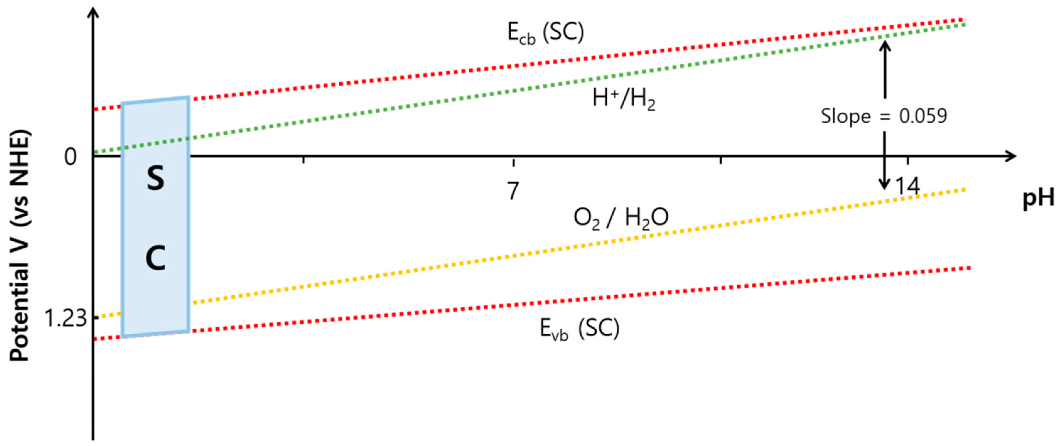
2.1. Requirements for Semiconductor Photoelectrodes

The semiconductor absorbers should satisfy the following fundamental conditions for WS: they should have proper conduction and valence band edge positions for water reduction or oxidation. An appropriate band gap and absorption coefficient is needed to include a large portion of the solar spectrum and efficient light absorption. In addition to these conditions, photoelectrodes should have good charge transport characteristic and durability in different operation conditions, such as acidic or basic electrolytes.
Knowing the band edge positions at the surface is important since they determine the maximum redox potentials of the photogenerated electron-hole pairs in a semiconductor [18], although the actual power for reduction or oxidation of electrons or holes is less due to the loss of energy in the space charge region (SCR) layer. The valence band (Ev) and conduction band (Ec) edge positions must straddle the water oxidation/reduction potentials. Semiconductors with the valence band maximum (VBM) below the water oxidation potential could be used as a photoanode in the water-splitting reaction and those with the conduction band minimum (CBM) above the hydrogen evolution potential could be used as a photocathode. Figure 1a shows the band gap and band edge positions of the various semiconductor materials with respect to a normal hydrogen electrode (NHE) and vacuum energy level [3,19,20,21]. Among group IV, group III-V semiconductors, i.e., Si, GaAs, GaN, GaP, and GaInP2, have feasible potentials for water reduction, and GaN and InP have proper potentials for water oxidation.
Other semiconducting layered materials, such as MoS2, MoSe2, WS2, WSe2, have appropriate band gap and band edge position for PEC WS, but are normally utilized as co-catalysts to enhance the PEC activities because of extremely short minority diffusion length. Therefore, layered metal chalcogenide materials are used as junction material for enhancing charge transfer or co-catalysts. When utilizing a single semiconductor as an ideal absorber, a 1.6 eV of band gap is needed, and the solar-to-hydrogen (STH) conversion efficiency can reach up to 30% [22]. However, there exist factors that limit the light absorption, hinder charge separation and injection, making it challenging to find an ideal semiconductor material.
Figure 1b illustrates the solar spectrum irradiance at 1 sun and an integrated fraction showing how much solar spectrum the semiconductor can absorb. A semiconductor absorbs shorter wavelength than its band gap, which are the spectrum in the integrated area to the left of the wavelength corresponding to the x-axis. Si has an indirect band gap of 1.12 eV, meaning that it can absorb a wavelength shorter than approximately 1127 nm according to λ = 1240/Eg (similarly, GaAs, 1.4 eV/886 nm and single-layer MoS2 1.8 eV/689 nm (bulk 1.23 eV/1008 nm) [23]. We calculated the portion of the solar spectrum that can be absorbed by these three semiconductors by integrating the solar irradiation spectrum above the wavelength. The result showed that among the three semiconductors mentioned above, Si can absorb 80%, GaAs 62%, and MoS2 50% (bulk MoS2, 75%) of the full solar spectrum. With large absorption portion of the sunlight, Si has advantages as a promising absorber for the WS reaction, which is long diffusion length and recombination lifetime induced from the indirect band gap.
In addition to the aforementioned requirements, one needs to consider the electrolyte, which can significantly affect the photoelectrochemical performance in the PEC system. According to the Nernst equation, the hydrogen evolution reaction (HER) and oxygen evolution reaction (OER) potential changes are proportional to the pH by 0.059 at the 1 atm. and 25 °C (Figure 2). Conversely, the semiconductor used as the photoelectrode might have a different slope compared to that of water. The Munich group revealed the redox shuttle mechanism of the CdS photoelectrode by following its reduction peak (conduction band position of CdS) according to the pH [24]. They illustrated that the rate of change in the reduction peak position of CdS was different from that of water, and thus showed that at high pH, the inversion of the CdS valence band edge and the scavenger redox couple occurred, leading to changing the redox mechanisms. Therefore, choosing materials depending on the band gap and band edge position mentioned earlier in Figure 1a may not yield the best performance if the pH of the electrolyte while operating is not considered. However, there are semiconductors, such as MoS2, and redox couples, such as Ce3+/Ce4+, Ag+/Ag, etc., that do not show pH dependence [24,25].

2.2. Properties of Si Photoelectrodes

Figure 3a illustrates the process of the water redox mechanism of a single n-type Si photoelectrode under illumination. Under the dark condition, a dynamic equilibrium is established as the majority carrier transfers from Si to the electrolyte, changing the electron energy states, and the Fermi level is adjusted, which induces band bending (built-in potential, Φ b i ) with an energy barrier height ( Φ B ) . The potential drop occurs mostly within the semiconductor surface (depletion region), while only a minor portion of the drop appears within the electrolyte, i.e., a voltage drop across the Helmholtz layer. The electrolyte’s redox couple energy with respect to the vacuum level is not accurately known but the theoretical and experimental values vary between 4.30 and 4.85 eV [26]. Usually, 4.5 eV is taken.
Under light illumination, when energy is larger than the band gap of the semiconductor (1.12 eV for Si), it is absorbed through the semiconductor, electron-hole pairs are generated, which is referred to as minority carrier injection. The minority carriers generated within the depletion region are forced by the inherent potential within the depletion region of Si and are swept away either toward the bulk or electrolyte, respectively. The electron-hole pairs generated within the quasi-neutral region (holes in n-type and electrons in p-type) diffuse toward the depletion region to be swept by the voltage drop. The driving potential of the depletion region is called a photopotential (i.e., photovoltage, Vph) and is induced by the shift of the Fermi-level within the depletion region, which is called the quasi-Fermi level (black dashed line in Figure 3a). The Vph was demanded to be the band gap of the semiconductor itself, which is (1/q)Eg, where Eg denotes the band gap of a semiconductor and q is an electronic charge. However, as shown in Figure 3a, the amount of Vph is smaller than the band gap, which is due to the recombination process. The maximum photovoltage limit (Vm) of a semiconductor is determined by the intrinsic bulk recombination, which can be expressed as follows [27]:
V ph = k T q ln ( J ph L n N A q D n n i 2 ) = k T q ln J ph J sr
where q is the electronic charge (1.6 × 10⁻¹⁹ C), Jph is the photocurrent density, Ln is the minority carrier (here, it is an electron) diffusion length, NA is the acceptor concentration, Dn is a diffusion coefficient, ni is the intrinsic carrier concentration, Jsr is the bulk recombination current density. In the case of silicon, the maximum obtainable Vph is calculated to be 0.48~0.50 V. However, much less than the maximum Vph of Si is easily observed with significant variations of more than 0.30 V, experimentally. This is due to the surfaces states on which the surface recombination takes place [28]. The states presented on the surface pin the Fermi level at the electrode/electrolyte in a dark equilibrium, which is called the Fermi-level pinning (FLP) effect, due to which the band bending is fixed such that no additional potential increase occurs under the external electrical field. As a consequence, the energy barrier formed at the electrode/electrolyte interface is lower than the theoretical maximum value (Vm), hindering efficient PEC operation (Figure 3b). Surface modification by using a catalyst to resolve this issue is thus crucial to enhance the overall cell performance. The role of the catalyst in terms of how it alters the energetics and kinetics of the cell are explained in the next section.

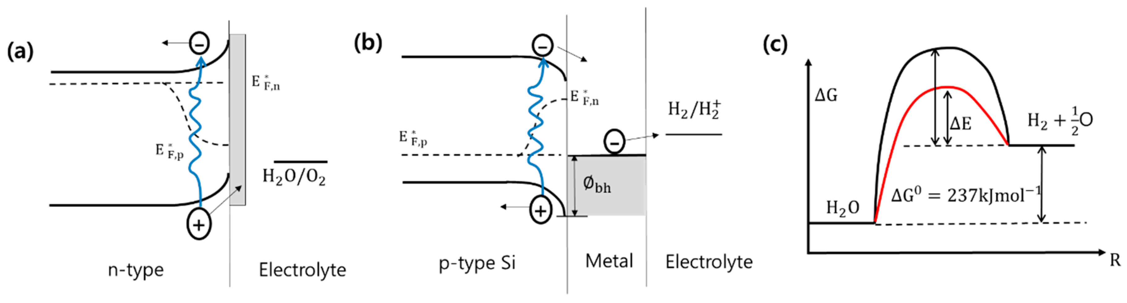
2.3. Co-Catalyst on Si

The key motivation of employing a photocatalyst or co-catalyst to Si is to lower the activation energies for surface electrochemical reactions. Figure 4c illustrates the thermodynamics of the WS reaction, 2H2O 2H2 + H2. It can be seen that the energy of ∆Go = 237 kJmol−1 is required to complete the reaction. However, additional activation energy (Ea) is needed to complete the uphill reaction. By applying the catalyst, the Ea barrier can be lowered (red line) with hinder a number of reaction. Pt has been known for low activation energies in hydrogen evolution reactions and has also proven to be the most efficient photocatalyst when integrated with semiconducting light absorbers [29]. The surface states prevailing on the semiconductor slow down the photogenerated charge transfer reaction, preventing electrons from being efficiently consumed [30]. When a catalyst is applied to the semiconductor (Figure 4a), the surface states remaining on the semiconductor are filled, suppressing the surface recombination, increasing both Vph and Jph.
In terms of recombination, moreover, the deposited catalyst layer can suppress the minority carrier tunneling through the triangular potential barrier in the semiconductor depletion region. Under the light, the quantitative understanding of the semiconductor/electrolyte junction is critical. For a quantitative understanding, Reichman et al. studied the effect of the surface charge density on the band bending in a semiconductor/electrolyte system, in 1980 [31], and Thorne et al. employed the equation to describe the charge transfer across the electrode/electrolyte interface [5] as follows:
n s n 0 = exp ( q Φ b k T ) = exp [ q ( V app + V ph V CB ) k T ]
where n s   and   n 0 are the electron densities under illumination and dark, respectively, q is the electronic charge (1.6 × 10 19 C ), k is the Boltzmann constant, T is the temperature in K, Φ b is the band bending, Vapp is the applied potential, Vph is the photovoltage and VCB is the conduction band edge. Equation (2) shows that the surface energy induces variation in the Fermi level position of the semiconductor, which largely pertains to the PEC performance, and mainly affects the amount of the onset voltage shift. Such surface band bending is also correlated with the charge transport from the bulk to the electrolyte in a complicated fashion [5]. Photo-generated charge kinetics that towards the electrolyte can be explained by the Butler–Volmer equation, as follows:
J n = J n 0 { n s n s 0 exp ( q α p k T ) exp [ q ( 1 α p ) η k T ] }
where Jn is the electron current density, J n 0 is the dark equilibrium current density, αn is the charge transfer coefficient and η is the overpotential. According to Equation (3), both the surface band bending and the kinetic factors affect Jph. The Jph can also be expressed by using Garner’s relation [32], which expresses the current density generated inside the depletion layer and in the adjacent bulk quasi-neutral region.
J ph = q J 0 [ 1 e α W 1 + α L ] q n 0 D n L n
Here, Jph is a photocurrent, J0 is a monochromatic photon flux incident on a semiconductor, α is the light absorption coefficient of silicon, W is the depletion region and L is the bulk diffusion length. To sum, one can conclude that the change in the surface charge density of the semiconductor by catalysts increases the band banding of the surface as well as the kinetics. The physical role of the catalyst is that it serves as a passivation layer from the solution environment of the semiconductor.
As for the metallic catalysts, they form the metal-semiconductor (MS) Schottky junction, whether nanoscale or microscale interfaces are created. If enough light penetration through the semiconductor is secured, this can increase the band bending in the bulk of the Si surface, which facilitates the electron-hole separation. As mentioned above, noble metals, such as Pt, have been considered to be the best candidates due to the lowest activation energy for H2 evolution. In other words, they possess high work function properties, with a greater ability to trap electrons compared to Si. Pt nanoparticles on Si NWs yield energy conversion efficiencies up to 8.14% [33]. A photoelectrode with Pt on semiconductors, such as a combination with CdS, and Si showed a quantum yield of approximately 60.34 % measured at 420 nm [34]. In Figure 4b, the induced barrier height ( Φ B ) due to the metal–semiconductor (MS) Schottky junction formed and this built-in electric field enhances Vph, helping the generated electron to be efficiently transferred to the electrolyte. Despite a number of studies on MS-based WS, the detailed explanations of how photocatalysts affect the PEC performance in terms of Jph onset potential are still not clear [35]. However, according to recent reports, it is evident that photocatalysts affect the surface energetics and kinetics of the semiconductor, thus enhancing both Vph the Jph [36,37]. In addition to the solid-state effect of the catalyst explained so far, the properties of the catalyst film itself obtained in the dark condition under HER or OER operation is also important, since a large portion of the kinetic effect stems from the electric and structural properties of the catalyst. In this context, unveiling both solid-state physics and electrochemistry in the co-catalytic systems is essential for the profound understanding of the desired PEC WS.

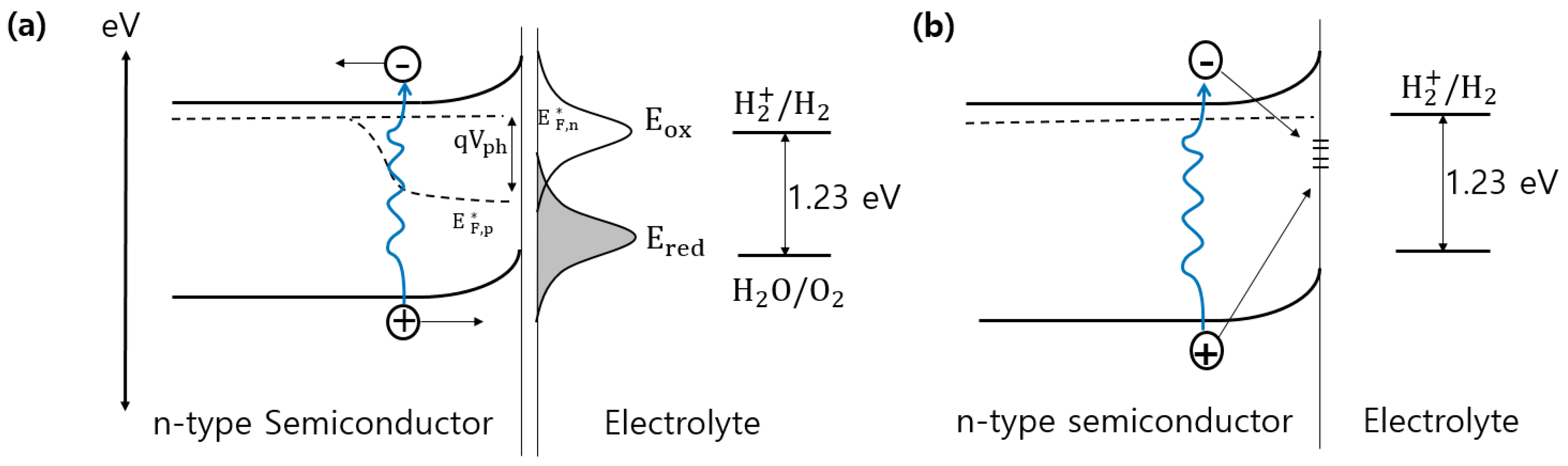
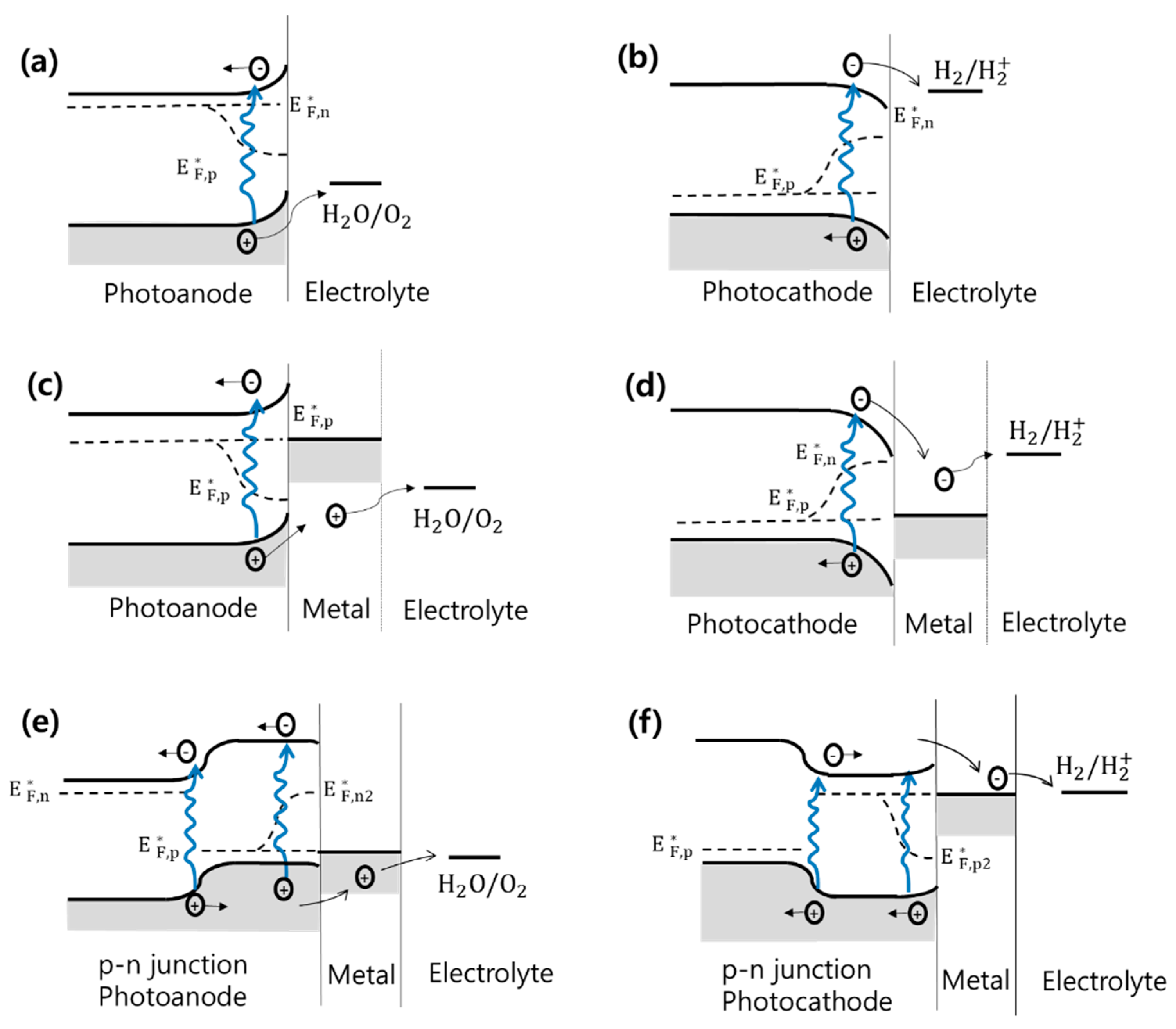
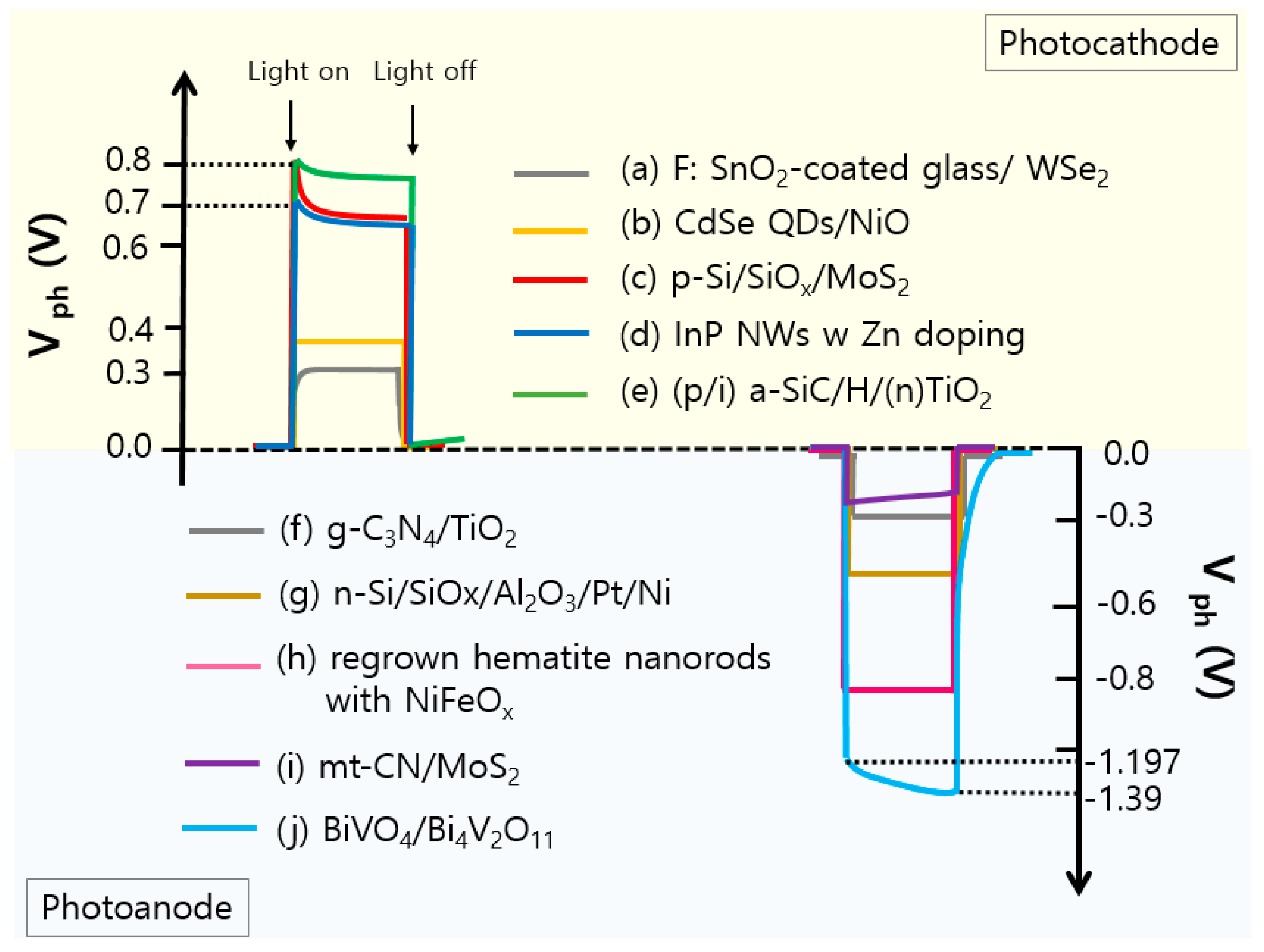
2.4. Photoelectrode Half-Cell Configurations

The energy band diagrams of different types of Si-based photoelectrodes and the operation under illumination are shown in Figure 5. The simplest configurations, which are solely semiconductors, are shown in Figure 5a,b for the photoanode and photocathode, respectively. The driving force of the generated electron-hole pair separation comes from the electric field at the junction formed at the electrode/electrolyte interface. In the photocathode, the generated electrons transport toward the electrolyte for the water reduction, while the generated holes are for the water oxidation in the photoanode. As a solution to overcome the low Vph induced from the semiconductor surface states, metal layers or islands are commonly deposited on the surface of the semiconductors, which forms Schottky contacts in the micrometer to nanometer scale domain (Figure 5c,d), which has been studied as an effective photoelectrode configuration for decades [38]. The deposited metal layer partially or fully protects the semiconductor surface in the physical dimension from the solution environment, providing enhanced Vph, which are independent of the redox potential of the ions in the solution [39]. However, for stable and longer time operations, the importance of the stable interface between the semiconductor and the catalyst layer interface has been gradually increased. Researchers started to apply a buried n-p junction with a catalyst deposited (Figure 5e,f), which provides the clean junction interfaces so that the facile electron-hole pair separation can occur. For this reason, multi-junction (both homo and hetero junction) thin film solar cell structures have been studied for over 20 years and have become mainstream in the field [40]. The buried junction configurations show the enhanced performances as photoelectrodes in the field of PEC that has occurred over decades. Further, improvements employing the multi-junction (both homo and heterojunction) thin-film solar cell structures have been studied for twenty years and have become a large research stream in the field. Electron-hole pairs are generated both near the surface and within the junction are depicted in Figure 5e,f. Note that since there is more than one junction presenting depletion layers, there exists a dominating one that determines the photovoltage of the cell [8,41,42]. Other types of cells, such as the PEC cell using organic (organic-inorganic hybrid) absorber [43], and tandem structure cells [44] are not included here.

3. Flat-Band Potential Measurement

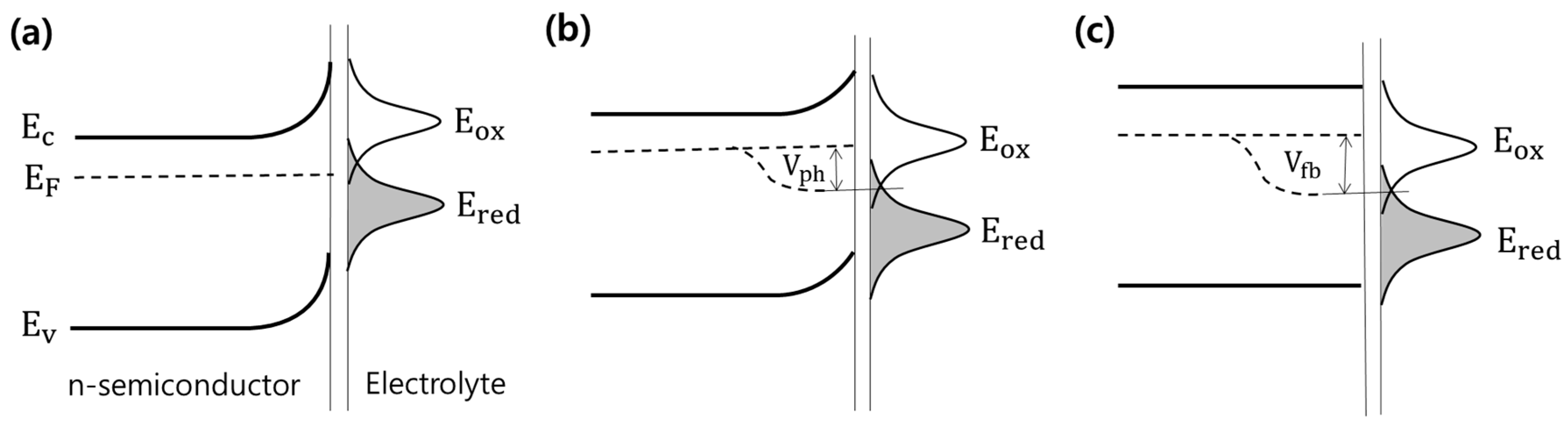
3.1. Concepts of Flat-Band Potential

Flat-band potential (Vfb) is an important and direct measure in the understanding of PEC experiments by clarifying the band structure of a semiconductor. The Vfb can be measured if an incident light illumination (Eg) is sufficiently intense to remove the band bending [45]. Figure 6 depicts the band banding change with a gradual increase of the induced Vph, where Eox and Ered are the electrolyte redox potentials and Ec is the conduction band, Ev denotes the balance band and EF is the Fermi level. Under the dark equilibrium condition, the Fermi level of the electrode is aligned with that of the electrolyte, which induces the band bending of the bulk semiconductors (Figure 6a). In Figure 6b, when the light is absorbed, the Fermi level splits into the quasi-Fermi level, where the difference is the Vph, and the band bending decreases due to the enhanced energy density states. As the light intensity increases, the band flattens at Vph, which is referred to as the flat-band voltage (Figure 6c). The flat-band potential gives information about the band bending at the dark equilibrium or built-in potential, in the case of a p-n junction. There are several methods to measure the flat band potential, some of which will be introduced below.

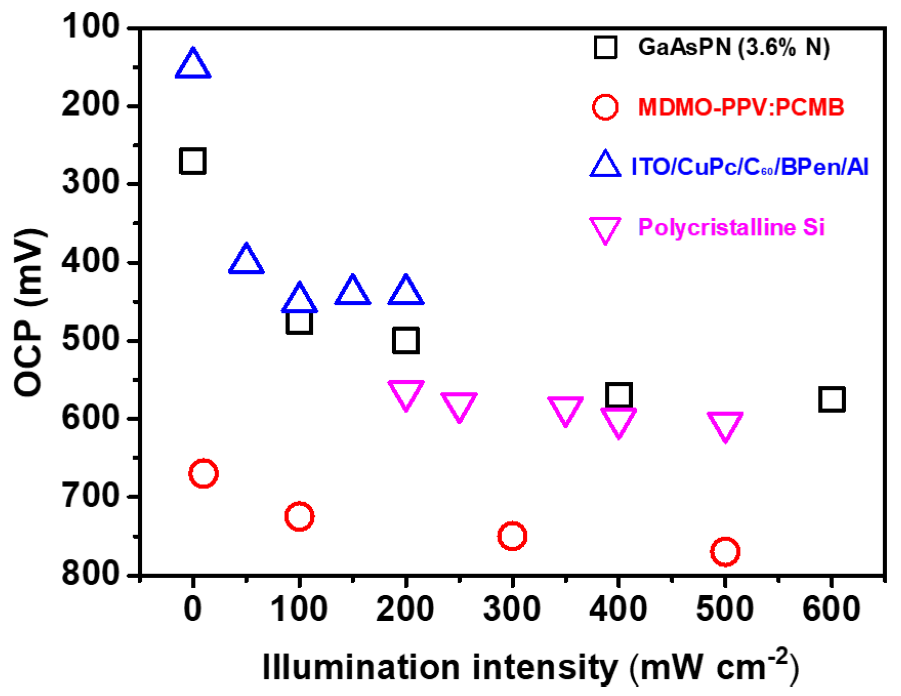
3.2. Illuminated Open-Circuit Potential (OCP)

The illuminated open-circuit potential (OCP) is a feasible way for determining Vfb when sufficient light is illuminated to remove band bending. This technique is an effective and convenient way to obtain the Vph of the electrode and gives useful information about the band bending and is commonly measured by increasing the light intensity until the Jph saturates [46].
Figure 7 depicts the OCP versus the illumination intensity to the samples of p-GaAsPN cell, MDMP-PPV:PCMB (bulk heterojunctions consisting of polyf2-methoxy-5-s38,78-dimethyloctyloxyd-p-phenylenevinylene (MDMO-PPV) and 6,6-phenyl C61-butyric acid methyl ester PCBM), dye-sensitized solar cell (DSSC) (ITO/CuPc/C60/BPen/Al) and polycrystalline Si. As the light intensity increases, the OCP value saturates, which means the bands became flatten. Note that the Efb of many semiconductors follows a Nernstian relationship as a function of pH.
The photovoltage can be obtained from Vph = VocphVocdark. Figure 8 illustrates the flat band potential measurement using the open-circuit potential difference of photoelectrodes in the electrolyte in the literature. The papers containing the measurements of the flat band potential were sorted and the values were grouped into photocathode (top) and photoanode (bottom). Note that the references include other catalytic materials besides transition metal (di)chalcogenide (TMD) materials. The positive shift in OCP upon illumination indicates that the semiconductor is p-type, whilst the negative shift in OCP indicates the n-type semiconductor. Yu, X, and Sivula, K presented a solution-processed multiflake WSe2 photocathodes coated with Al2O3 layer showing ~ 0.3 V of Vph [51], which was drawn in the black line indicated with (a). The yellow line marked with (b) shows the Vph measurement of the CdSe quantum dots with nickel oxide (NiO) engineered by a molecular liner, mercaptoacetic acid (MAA) [52], which is below 0.4 V. For the red line (c), the photoelectrode of p-Si/SiOx/MoS2 photoelectrode in a pH = 0.3 H2SO4 also showed significantly high photovoltage of 0.8 V [53]. The sharp decrease of the photovoltage upon illumination is attributed to bulk recombination within the electrode. The photovoltage is directly correlated with the onset voltage of the J (photocurrent density) – V (voltage) characteristic of the PEC performance). Kornienko et al. developed the growth of InP NWs and demonstrated the integration on Si substrates. With Zn doping, the NWs exhibited 4.0 % of light to hydrogen efficiency in a half-cell configuration, showing ~0.7 V vs RHE of flat band potential [54]. The high photovoltage of 0.8 V was obtained by using p-type/intrinsic hydrogenated amorphous silicon carbide (a-SiC) photocathode combined with TiO2 (Figure 8e) [55]. The high Vph was explained by the p-i-n heterojunction structure produces the internal electric field that enhances the photovoltage. As for photoanodes, a well-ordered TiO2 nanotube arrays (TNAs) decorated with graphitic carbon nitride (g-C3N4) were fabricated by Liu et al. and the photovoltage was measured to be 0.26 V under light irradiation [56]. The highest photovoltage was obtained by dos Santos, W.S. et al., who introduced an efficient approach which is coupling ferroelectric materials with semiconductors to boost the photovoltage higher than that obtainable from a conventional p-n heterojunction. The ferroelectric Bi4V2O11 perovskite and n-type BiVO4 creates a virtual p-n junction that produces high photovoltage of 1.39 V (Figure 8j) [46]. The metal-insulator-semiconductor (MIS) photoanode using silicon was fabricated by Digdaya et al. [57]. The n-Si/SiOx/Al2O3/Pt/Ni photoanode with 0.49 V of photovoltage was obtained after 18 h aging, which is indicated in brown color marked (g). The MoS2/S-doped g-C3N4 heterojunction film for a photoanode was introduced by Ye et al., showing ~0.2 V of photovoltage [58]. The high photovoltage value of Figure 8h demonstrates that hematite photoanode exhibits good PEC performance. Furthermore, the measurement of the OCP decay after the removal of the light source can provide information about the excess carrier lifetime in p-n diodes or solar cells [59,60]. Using the short-term high frequency measurement and the OCP decay method in a long-term time-scale observation, the OCP decay measurement provides information related to the electrode/surface recombination mechanism along with the minority carrier lifetime in Equation (5) below [61].
τ h = k T q ( d V oc d t ) 1
Equation (5) can be applied under the condition of a low-injection level so that the relationship between the Fermi level variations with time and the minority carrier concentrations expand in the first-order linear differential equation [62]. Studies using this technique can be found in other applications in dye-sensitized and perovskite solar cells.

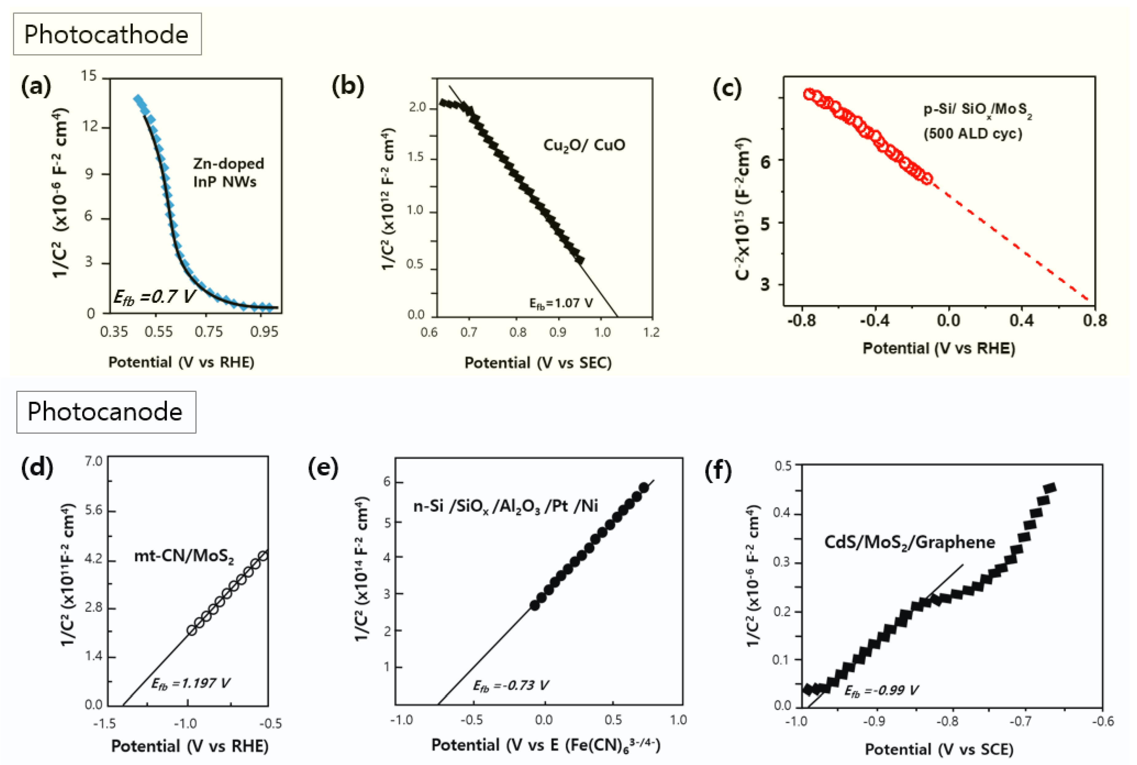
3.3. Mott–Schottky Analysis

Another powerful method is a Mott–Schottky (M–S) plot, by which the Vfb or built-in potential for p-n or Schottky junction interfaces can be determined. In semiconductor electrochemistry, the M–S plot describes the capacitance value versus the potential difference between bulk semiconductor and the electrolyte. Therefore, from the M–S plot, the qualitative analysis of the conductivity types and the carrier concentration of semiconductors can be obtained [63]. The positive slope in the linear region indicates the n-type nature, while the negative slope indicates the p-type nature. In accordance with Equation (6), the carrier concentration is derived from the reciprocal of the slope in the plot and the x-intercepts from the linear portion fitted (over 200 mV range minimum) is the flat-band potential induced from the bulk interface between the electrode and electrolyte or bulk built-in potential. ε r is the relative permittivity of the semiconductor (11.7 for Si), ε 0 is the permittivity in vacuum, A is the surface area, e is the electron charge, Ndopant is the carrier density, k is the Boltzmann constant, T is the temperature, and V is the applied voltage. From the slope, the conductivity type, the Ndopant as well as the depletion layer width, which are the surface properties of the semiconductor, can be calculated.
1 C sc 2 = 2 ε r ε 0 A 2 e N Dopant ( V V fb k T e )
Figure 9 shows the Mott–Schottky measurement of various types of photoelectrodes to obtain the flab-band potential. Ye et al. reported a MoS2/S-doped g-C3N heterojunction film for high visible-light photoelectrochemical (PEC) cell (Figure 9a) [58]. The Mott–Schottky curve was obtained at a frequency of 10 kHz, showing the positive slope, an indication of the n-type characteristics with the flat-band potential of 1.197 V. A Mott–Schottky plot of the MIS devised with Pt/Ni catalyst in KOH solution is shown in Figure 9e. The flat-band potential of −0.73 V was determined [57]. Yua et al. carried out Mott–Schottky measurement in a solution containing 0.5 M Na2SO4 to determine both flat band potential and donor density at semiconductor/liquid interface. The n-type semiconductor properties of CdS/MoS2/graphene hollow spheres were confirmed [64]. Photocathode using Zn-doped Indium phosphide nanowire arrays showed a flat band potential of ~0.7 V vs reversible hydrogen electrode (RHE), which was consistent with their OCP measurement [54]. In Figure 9b, Cu2O/CuO bilayer composites were prepared and tested as an efficient photocathode and the M–S plot confirmed ~1 V of flat band potential, implying a high degree of band bending and a large depletion layer (i.e., SCR) [65]. p-type Si/SiOx/MoS2 layer photocathode also revealed significantly high flat band potential of 0.8 V as shown in the Figure 9c. Considering that the catalyst or co-catalyst modify the surface energetics, the Mott–Schottky technique provides information on the surface energetics of the semiconductor, the effect of the catalyst has been exploited by researchers [66,67], and the Si photoelectrodes decorated with TM(D)C materials to determine the Vfb have also been analyzed and were proven to be informative in understanding the change in surface properties of Si [68,69,70]. In Figure 9, the change of the surface doping density and the depletion width of the p-Si with the MoS2 catalyst layer thickness was observed, which induces the different Vfb potential.
In PEC WS, flat-band potential which can directly identify the band structure of the semiconductor in a junction with the electrolyte can be measured with two powerful methods, OCP and M-S plot. The photovoltage is important because it is directly correlated with the onset voltage of PEC performance characteristic. In the next section, the other important properties including charge transfer dynamics will be discussed with electrochemical impedance spectroscopy as a measurement tool.

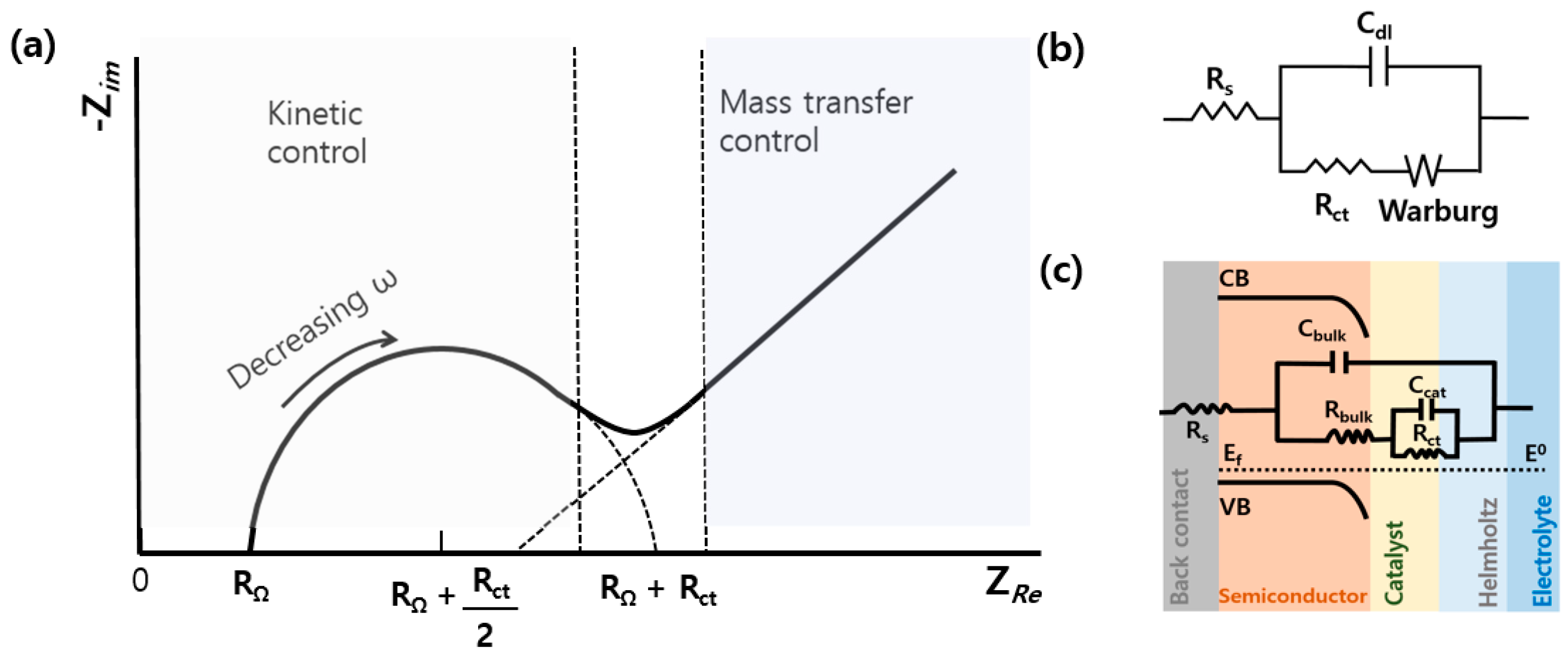
4. Electrochemical Impedance Spectroscopy (EIS) for Photoelectrochemical (PEC) Cells

Electrochemical impedance spectroscopy (EIS) is a powerful technique to feature electrochemical behaviors through the whole electrochemical cell including the electrode/electrolyte interface. We could extract meaningful quantitative and qualitative information in terms of impedance sources within the cells such as solution resistance, charge transfer resistance, and mass transfer. There are two main analyses in EIS, i.e., the Bode and the Nyquist plots. The Bode plot shows the response to the frequency in a system, so the magnitude and phase plots can be obtained at the same time. The Nyquist plot, on the other hand, shows gain and frequency at the same time on the graph, explaining gain for all frequencies. Therefore, the information of bulk charge electrochemical reaction at high frequency and interface charge transfer dynamic at low frequency can be obtained through a Nyquist plot. In this section, we explain how to obtain useful information from the Nyquist plot in the simple model of the PEC cell.
Through the measurements, the impedance data measured in the electrochemical cell can be expressed and analyzed by the system of resistors and capacitors in an equivalent circuit [71]. An electrochemical cell consists of an electrolyte solution and electrode. The Faradaic impedance Zf is the resistance and capacitance acting mutually at the electrode surface and can be divided into the charge transfer resistance (Rct) which describes the kinetics of the electrochemical reactions at the electrode/electrolyte, the Warburg impedance (ZW) which represents a mass transfer, and the ohmic resistance of the solution, back contacts, etc. If the solution is not electroactive species, the observed impedance is called the non-Faraday impedance.
The surface kinetics of an electrode can be investigated via the frequency spectra of real and imaginary components of the system in the solution. The two-electrode configuration provides the information of the overall charge transfer occurring from the semiconductor to the counter electrode through the electrolyte, while the three-electrode configuration the information of the semiconductor/electrolyte interface and the double layer [72]. The three-electrode configuration gives a more detailed analysis of the electrode/electrolyte interface compared to the two-electrolyte configuration, since the impedance data of both electrodes can be overlapped in the case of the two-electrode configuration. In the PEC system, the EIS measurements are commonly conducted under dark, illumination, and under applied voltage if needed. The measurement is generally recommended to be carried out by scanning the cell from a high frequency (50~100 kHz) and sweeping to a lower frequency (10 mHz). With the EIS data, one can identify and separate the two different layers, which respond at different frequencies. The high-frequency range provides information of the effect of the bulk matrix to the electrochemical reaction, while the low frequency range provides information of the double layer capacitance [73]. Figure 10a shows the typical Nyquist plot of the working electrode of three-electrode cell. A semicircle at high frequency and the diffusion process at the low frequency edge appear, the mixed control process model known as Randle’s circuit (Figure 9b). From the plot, one can obtain the values for resistance as well as the capacitance which are often replaced by constant phase element (CPE). The capacitive impedance is short-circuited when the ω→∞ so only RΩ remains at the high frequency plot. EIS of photoelectrodes are measured either in or un-bias within the range from 100 kHz to 10 mHz under the illumination or under dark. It is important to choose the correct model because the semiconductor/electrolyte has a complex system such as capacitance of the SCR, surface states, and the Helmholtz layer (as a constant phase element). Figure 9c illustrates an example of the energy diagram of a photocathode/electrolyte interface with the corresponding electrical equivalent circuit, where Cbulk and Rbulk represent the SC layer components and Ccat and Rcat indicate the charge transfer from the catalyst to the electrolyte. For a Si/TMD photoelectrode, Andoshe et al. deduced the charge transfer resistance from TiO2 thin film to electrolyte through a MoS2 catalyst and found that the value is smaller compared to the charge transfer resistance from TiO2 to electrolytes, confirming that the photogenerated carriers from p-Si can effectively be transported to the TiO2 and 3D MoS2 layers [74]. Thorne et al. utilized intensity modulated photocurrent spectroscopy (IMPS) to investigate the origin of the performance enhancement and observed that the deposition of the NiFeOx layer suppressed the surface recombination, while there was no contribution by fast hole transfer kinetics [35]. Ding et al. demonstrated the enhanced adhesion between the MoS2 catalyst and Si by measuring the charge resistance of the interface through EIS [75]. More efficient charge transfer characteristics of 1T MoS2 than 2H MoS2 was also confirmed. For MoS2 photocatalyst, researchers including Ho et al. observed the correlation between HER activity and exposure level of MoS2 edge site, which helped to embody the effect of MoS2 structural characteristics on HER performance [76]. The charge transfer characteristics and the internal resistance of the TM(D)C material combined with Si have been studied by many researchers [77,78,79] revealing the relationship between the surface modulation and kinetic enhancement. In the case of Si photoelectrode modified by MoS2, the performance and catalytic properties tend to be affected by its thickness [79,80].
The EIS analysis also provides relevant information regarding the zone where charge accumulation occurs at the bulk and the electrode/electrolyte interface. Depending on various preparation methods such as annealing and surface treatments, the catalysts may have different or mixed phases. These surface morphology, phase and thickness features of the catalyst can be factors affecting the charge transfer kinetics. The photoelectrode with the thicker layers of TM(D)C materials show higher resistance but can exhibit lower charge transfer resistance values at the electrode/electrolyte interfaces, showing better performances [75,81].

5. Si/Si/Transition Metal (di)Chalcogenides [TM(D)C] Photocathode

It is surprising that the number of the studies of PEC WS on the heterostructures of Si/TM(D)C were limited to date although TM(D)C materials and Si photoelectrodes themselves were studied extensively in the literature. The resulting PEC HERs in acidic media show superior performance when compared to those in alkaline media since the kinetics in an alkaline electrolyte is often limited by the sluggish water redox reaction steps [54]. Most Si-based PEC-WS employs overlayers of metals or metal oxides because of the poor stability when operating in aqueous electrolytes. Metal chalcogenides on Si for PEC-WS has been studied since 2012, when explosive MoS2 research activities as a post-graphene have begun. Narrowing down the scope to Si as an absorber which is known to be the best and widely used in industry, there was about 10 reports on TMDC on Si, and about 27 papers on Si/TMC until now. Note that only one paper has published for photoanode, and Si is more suitable for use as a photocathode as in Figure 1a. We categorized all types of the Si/TM(D)C photoelectrodes published into the following issues: (1) whether they are layered or non-layered; (2) types of Si such as n, p-type and n+p buried junction; (3) employing interlayers between Si and TM(D)Cs. The results are summarized in Table 1 and Table 2.
Tran et al. utilized MoS2 layers on p-Si nanowire (NW) arrays where 1-D nanostructures have several advantages for PEC water splitting due to their excellent charge collection efficiency and high surface area [82]. They deposited MoS2 on Si NW by photo-assisted electrodeposition methods. Photoelectrochemical measurement was conducted in 1.0 M Na2SO4 buffer (pH = 5.0) solutions under 1 sun illumination. It showed + 0.25 V vs. RHE onset potential which is an anodic shift of 0.55 V considering bare p-Si onset potential (−0.3 V vs. RHE), and photocurrent density was 1 mAcm−2 at 0 V vs. RHE. It was stable during 1 h of PEC operation. The superior hydrogen generation performance compared to that of a planar Si was attributed to the lower kinetic overpotential induced from the high surface roughness. The Song group studied with chemically exfoliated chemical vapor deposition (CVD) grown MoS2 conjunction with p-Si wafer that showed the possibility of MoS2 as a replacement of noble metal like Pt [75]. MoS2 was deposited by CVD at 475 °C which is the most popular way to grow 1T MoS2. The PEC measurement was conducted with the solution of 0.5 M H2SO4 (pH = 0.3) under 1 sun irradiation and the resulting current density of 17.6 mAcm−2 was shown at 0 V vs. RHE twice higher than that of 2H phase (9.2 mAcm−2). Onset potential of 1T MoS2/Si was 0.25 V vs. RHE (2H MoS2/Si was 0.23 V vs. RHE).
MoS2/p-Si structures as ALD-grown MoS2 on p-Si were also studied for HER by Oh et al. [78]. They investigated the number of ALD cycles and post-sulfurizing temperatures for crystallization to the resulting PEC performance. The optimum thickness and annealing temperature were 14 nm (590 cycles) and 600 °C, respectively. With the optimized thickness of MoS2 layers, they obtained 0.23 V vs. RHE onset potential and 21.7 mAcm−2 photocurrent at 0 V vs. RHE. They also exhibited good stability that only 10% decrease of current density after 24 h operation. The Jang group also reported MoS2/p-Si photocathodes which showed the best performance among all. MoS2 was synthesized with spin coating of (NH4)2MoS4 and subsequent CVD process at 950 °C. Onset potential was relatively low (+0.17 V vs. RHE.) but photocurrent at 0 V vs. RHE was 24.6 mAcm−2. It was also stable during 10,000 s during PEC operation [81]. Joe et al., found that the mixed-phase MoS2 could improve the Si photocathode for PEC WS by regulating the systems impedance [53].
The Liu group fabricated unique structures of MoS2/Ag@Si nanosphere (NS) photocathode. Ag films were deposited on Si and dewetted into spherical shapes, then depositing Si again. Ag@Si NS template improved charge transfer significantly. It showed 0.11 V vs. RHE onset potential and photocurrent density −13.4 mAcm−2 at −0.04 V vs. RHE [83]. The Tsang group utilized WS2 with Si absorber. The WS2 layers were fabricated by magnetron sputtering on p-type Si, followed by annealing at 800 °C. Then Au was then deposited on WS2 for enhancing photo-activity and stability. They obtained low current density (0.37 mAcm−2 at −1 V vs. RHE) than MoS2. However, it was much higher than other oxides such as TiO2 or WO3 [84].
In addition to forming heterojunctions on p- or n-Si directly, improved photovoltages via a homojunction of Si was studied using n+p type buried junction combined with co-catalyst. In 2014, the Jaramillo group first reported n+p Si conjunction with MoS2. Mo3S13 nanocluster was imposed to enhance the catalytic activity of MoS2/n+p-Si photocathodes. MoS2 was thermally sulfidized after Mo sputtering on n+p-Si. Onset potential was 0.32 V (at −0.5 mAcm−2) vs RHE. and photocurrent density was 17 mAcm−2 at 0 V vs. RHE. Obviously, onset potential was improved at least +0.1 V than MoS2/p-Si configuration [85]. King et al. proved remarkably long duration of 24 days of stable operation under a continuous illumination condition is possible by interfacial engineering between the Si and MoS2 co-catalyst [86].
Huang et al. fabricated sputtered 2D MoSe2 directly on n+p-Si for hydrogen generation. It showed the best onset potential of +0.40 V vs. RHE and high saturated current density of 29.3 mAcm−2. Their PEC measurement was conducted under 1 sun illumination with the solution of 1.0 M HClO4. It also showed negligible change after 120 h. operation. This result is the only reported Si photocathodes with layered MoSe2 [87]. They attributed the PEC properties to the nearly vertically standing two dimensional MoSe2 layer as well as the sharp interface to Si.
To ensure stable operation, protecting Si from degradation in electrolyte is the most important step in the developments of Si-based photoelectrodes. As for protection, metal oxides such as TiO2 were commonly used. In TMDC/Si photocathode, TiO2 interlayer was also used for enhancing stability. The Yang group presented photocathode MoS2/p-type Si NW with interlayer of 30 nm ALD-TiO2. The MoS2 layer was synthesized with thermolysis method using (NH4)2MoS4. They obtained onset potential of 0.30 V vs. RHE and current density was 15 mAcm−2 at 0 V vs. RHE. It was stable under 1 sun illumination and 0.5 M H2SO4 acidic condition for an hour [88]. The Jang group also fabricated 3-D MoS2 on TiO2/p-Si by metal-organic CVD (MOCVD) processes. A large fraction of deposited MoS2 was vertically aligned and its grain size was relatively small (<10 nm). Their cathodic performance was better than their previous results when using 2D MoS2. It recorded 28 mAcm−2 at 0 V vs. RHE of the highest current density in TMDC/Si photocathode and onset potential was +0.35 V vs. RHE. It was stable for ~181 h in the solution of 0.5 M H2SO4 due to the role of TiO2 passivation layer [74]. The Zheng group combined both buried n+p-Si and interlayer Al2O3 for hydrogen evolution. The MoS2/Al2O3/n+p-Si configuration showed the onset potential of 0.40 V vs. RHE and saturated photocurrent of 35.6 mA−2. Their results exhibited the best onset potential compared to other TM(D)C/Si photoelectrodes, which came from the presence of Al2O3 interlayer worked as a protective and passivate layer during MoS2 deposition. It also exhibited best stability about 120 h operation under 1.0 M HClO4 (pH = 0) acidic condition [77].
In 1995, a group in India reported the first Si junction with metal sulfides photocathode. A n-Si foil was grounded and mixed with CdS and ZnS. Metal chalcogenide (CdS and ZnS) was made by Na2S and Cd(CH3COO)2 or Zn(CH3COO)2 precipitation method. When 7% of CdS mixed with n-Si, it showed best efficiency of 7.23 mLh−1g−1 [89]. After this report, the TMC/Si photoelectrode study stopped publishing. Similar with TMDC/Si photoelectrodes, however, reports on the TMC/Si photoelectrodes were also increased after 2011. Mo3S4 was synthesized by the drop-casting method on p-type Si wafer and nanopillar (NP). The p-Si substrate with Mo3S4 photocathodes exhibited the onset potential of +0.15 V vs. RHE and photocurrent of 8 mAcm−2 at 0 V vs. RHE. It was increased to 9 mAcm−2 at the same potential by changing p-Si wafer to p-Si nanopillar. The resulting Mo3S4/p-Si cells were stable for 60 min under red light illumination (power density 28.3 mWcm−2, wavelength > 620 nm) in 1.0 M HClO4 (pH = 0) [90].
Hou et al. decorated molybdenum-sulfur clusters on p-Si NW for hydrogen production. The clusters were synthesized with precipitation method in a chemical bath at 96 °C. This showed great PEC activities in the visible-infrared wavelength regions. The PEC measurements were conducted under 27.3 mWcm−2, at wavelengths > 590 nm. It exhibited the photocurrent of 14.3 mAcm−2 at 0 V vs. RHE and onset potential of 0.25 V vs. RHE. Expanding wavelengths to ~450 nm, photocurrent increased over 30 mAcm−2 at 0 V vs. RHE. It showed stable WS for ~3 h in H2SO4 (pH = 0.3) solutions [91]. Si NWs decorated with MoS3 was demonstrated by Huang et al. showing enhanced performance in comparison with SiNWs, with a photocurrent density of ~24.8 mAcm−2 and 0.37 V of onset voltage [92]. The binary and ternary TMCs on Si are also reported as photocathodes. Photo-assisted electrodeposition of NiCoSex on p-Si NPs were introduced. The molar ratio of Ni, Co, Se was 1:1:4.5 with amorphous structures. The PEC characteristic of a-NiCoSex/p-Si NP was the onset potential of +0.25 V vs. RHE and the highest photocurrent of 37.5 mAcm−2 at 0 V vs. RHE. After 2 h of the PEC test, photocurrent density decreased 9% [93]. The Barber group reported amorphous CoMoSx (a-CoMoSx)/p-Si photocathode. CoMoSx was synthesized with a photo-assisted electrodeposition method, using [Co(MoS4)2]2− solution. It showed the photocurrent of 17.5 mAcm−2 at 0 V vs. RHE and onset potential of 0.25 V vs. RHE under phosphate electrolyte (pH = 4.25). The photocurrents were decreased less than 5% after 3 h PEC operation [94]. The n-Si photocathode with TMC was first reported by the Shelke group. The n-Si NW was decorated with CdSe quantum dot (QD) by successive ionic layer adsorption and reaction (SILAR) methods under inert condition. The WS results showed size dependency with the CdSe cycles and it showed the maximum current of 6.1 mAcm−2 at 1 V vs. RHE. However, QD coverage was not enough to stabilize n-Si NWs under 0.25 M Na2S and 0.35 M Na2SO3 electrolytes (pH = 11.5), which significantly degraded in a minute [70].
The Liu group studied Co-based metal chalcogenides on Si photocathode. First, CoS2 co-catalyst on p-Si microwire (MW) was introduced for PEC hydrogen evolution. CoS2 was prepared with sulfidation of chemically synthesized CO(OH)2 on Si MW at 500 °C. It showed the photocurrent of 3.22 mAcm−2 at 0 V vs. RHE and onset potential of 0.249 V. It maintained photocurrent for 3 h operation under 0.5 M H2SO4 (pH = 0.3) solutions and 1 sun illumination [95]. They also compared stability and functionality of co-catalyst CoS2, CoSe2/p-Si MWs under 1 sun with various pH of electrolytes, i.e., 0.5 M H2SO4 (pH = 0.3), 1 M phosphate buffered saline (PBS, pH = 7.4), and 1 M KOH (pH = 13). CoS2 was not stable in alkaline solution, but CoSe2 was stable for 50 min. However, both were stable under acidic condition, especially CoS2 was stable for 9 h [96]. Improved photocurrent of 9 mAcm−2 at 0 V vs. RHE with onset potential of 0.18 V were obtained from CoSe2/p-Si MW which was prepared in the identical method with CoS2. After stability test of 50 cycles, it showed similar current density [97]. Finally, they prepared CoTe2/p-Si MW by drop casting, and 10 nm of ALD-TiO2 was deposited on CoTe2/p-Si in order to stabilize CoTe2 which is easily oxidized in ambient condition. It showed the onset potential of 0.17 V vs. RHE and saturated current density of 24.0 mAcm−2 [98].
The interfacial layers of metal oxides were also applied in the TMC/Si photocathodes. Seger et al. studied MoSx/Ti-TiOx/n+p-Si where Ti was used as a conductive and protection layer on Si. MoSx was deposited with the electrodeposition method, Mo and S atomic concentration was similar revealed by XPS. By protecting Si with Ti layers, the resulting onset potential was reached to 0.33 V vs. RHE and it showed current density of 12 mAcm−2 at +0.20 V vs. RHE and was stable for 1 h [99]. The Shen group synthesized MoS2 by photoreduction-annealing method, and 2 nm-thick Al2O3 was deposited on the n+p-Si for transparent and protect the Si surfaces from oxidation. The photoelectrochemical performance was 28.9 mAcm−2 at 0 V vs. RHE in current density and +0.35 V onset potential. Due to the Al2O3 protection layer, MoS2/Al2O3/n+p-Si photocathode was stable for 40 h [69]. The Huang group also reported photoanodes of p-Si with metal sulfides. The Ag2S/ZnS/ZnO/p-Si nanocones (NCs) were used and compared with ZnS/ZnO/p-Si and ZnO/p-Si NCs. The ZnO was prepared with the hydrothermal method at 90 °C, and by sulfidation with thioacetamide in a solution, ZnS was fabricated in the form of film. After then, Ag2S nanoparticles were decorated on top of the cell. Better band alignment with Ag2S/ZnO resulted photocurrent of 58.8 μAcm−2 at 2.1 V vs. RHE and it was 2.5 times higher than ZnS/ZnO/p-Si NC [100].
The TM(D)C/Si photoelectrode described above has limitations in terms of instability and low photovoltage. There are possible ways to improve the overall performance (1) by improving the coverage of co-catalysts and (2) by enhancing charge transfer and photovoltage drop through a junction with TM(D)Cs. By analyzing the current trends in Si/TM(D)C photocathodes, less than 40 studies have been reported so far, which means that there are still so much room to explore in this field. We suspect that one of the reasons why studies on Si/TM(D)C photocathodes have been limited would be the lack of reliable deposition methodologies. In the next section, we highlight atomic layer deposition techniques as a unique tool for growing TM(D)C on semiconductor absorbers.

6. Atomic Layer Deposition (ALD) of TM(D)C

6.1. Defect Chemistry of TM(D)C and Its Implication on Low-Temperature ALD

All synthesized materials inevitably include various types of defects at thermal equilibrium although the origins are different from each other. The defects can be divided into three distinctive categories, as follows: 0-D defects (point defects), 1-D defects (line defects), and 2-D defects (surface defects). In particular, point defects are of paramount significance to determine several properties such as conductivity, luminescence and Fermi level. The simplest point defect is caused by missing an atom or ion, called lattice vacancy (also known as Schottky defects). In another case, when the atom missed from a lattice site transferred to an interstitial position, we called it a Frenkel pair (i.e., a couple of two point-defects: an interstitial and associated vacancy). The probability of those point defects follows the Boltzmann factor leaving the home lattice-sites at thermal equilibrium: P = exp(−Ev/kBT), where Ev = energy for taking an atom from the lattice site on the surface. Therefore, the equilibrium concentration of point defects often pertains to the synthesis temperatures at the final stages. Controlling point defects is critical in many materials for industrial applications; fine control over the amounts of defects for tuning the electronical and optical properties is greatly important in technological applications. One could create these fine states by additionally doping other elements or by specific synthesis conditions. In TiO2 synthesis, for example, it has n-type property due to the energetically favorable formation of oxygen vacancies under ambient conditions [101]. In both anatase and rutile TiO2, the conduction band is predominantly made up from Ti 3d states, which are formally unoccupied in the stoichiometric material. These Ti valence states are highly localized, and the formation of intrinsic n-type defects donates electrons to the Ti lattice, occupying conduction bands to produce the localized defect states as observed experimentally [102,103].
Note that chalcogenide semiconductors have distinctive point defects such as anti-site defects, because they have a low vacancy formation energy, unlike those of oxide semiconductors. It has been shown that the precise control of conductivity can be achieved through the fundamental differences in the energetics of native defect formation in the Bi-Te-Se ternary system, for example [104]. In such chalcogenides, there are two kinds of charged defects: The substitutionary anti-site defect ( B i Te   or   B i Se ) and the vacancy defect ( V Te / V Te   or   V Se / V Se ). The effective charge carrier density could be expressed by neff = [ B i Te ] 2 [ V Te ] which is distinctive in that the dominant type of defects is determined by the thermodynamically stable anti-site defects when compared with a typical Frenkel pair ( T e Te X V Te + T e i ) in accordance with Kröger–Vink notation. In the stoichiometric Bi2Te3, B i Te has the theoretically lowest formation energy to be 0.4–0.5 eV among the charged defects. Therefore, the stoichiometric Bi2Te3 is the nominal p-type semiconductor. The stoichiometric Bi2Se3 has the vacancy defects of V Se / V Se that are thermodynamically stable charged defects, resulting in n-type properties.
In practice, however, the most popular synthetic method, CVD (as shown in Table 2) employ high growth temperatures of at least 600 °C, and the precise controls over the number and the type of point defects are very difficult. The amounts of point defects are exponentially affected by the Arrhenius equation in terms of temperature, K. The representative example is that the stoichiometric Bi2Te3 (as mentioned above, nominal p-type) has been reported as n-type semiconductor as a result of high growth temperature. As for the TM(D)C materials, therefore, understanding and controlling defects and defect processes is of significance at low temperatures.
Indeed, the perfect stoichiometric Bi2Te3 as a binary end compound is a representative example of TM(D)Cs that should be p-type [105] because of the low formation energy of anti-site defects, B i Te [106]. Like a number of TM(D)C materials, it is difficult to find the successful growth of intrinsic p-type Bi2Te3 in the literature because most of the system is prepared at high temperatures and Te vacancies are created easily. The migration energy for the Te vacancy is also quite low (ETe = ~1 eV), indicative of a high vapor pressure [107]. Recently, some of the authors reported that Bi2Te3 can be synthesized at temperatures as low as 100 °C (100–250 °C) through ALD chemistry and synthesis conditions. By varying the growth temperature, remarkably, Bae et al. observed the gradual defect activation from the nominal p-type to n-type in Bi2Te3 without any alloying, as shown in Figure 11 [13]. This result provides an insight on the understanding of doping properties by both nanostructuring (i.e., phonon engineering) and control of defect activation (i.e., electron engineering). Defect control activation with growth temperature can be adjusted to the PEC WS systems. By controlling defects and doping mechanism with temperature, we can control the charged point defect which can provide a recombination center and catalytically active sites. In conclusion, TM (D) C synthesis, which can show critical functions on the surface, is suitable for low temperature synthesis ALD process which can control defect rather than high temperature synthesis which defect control is impossible.

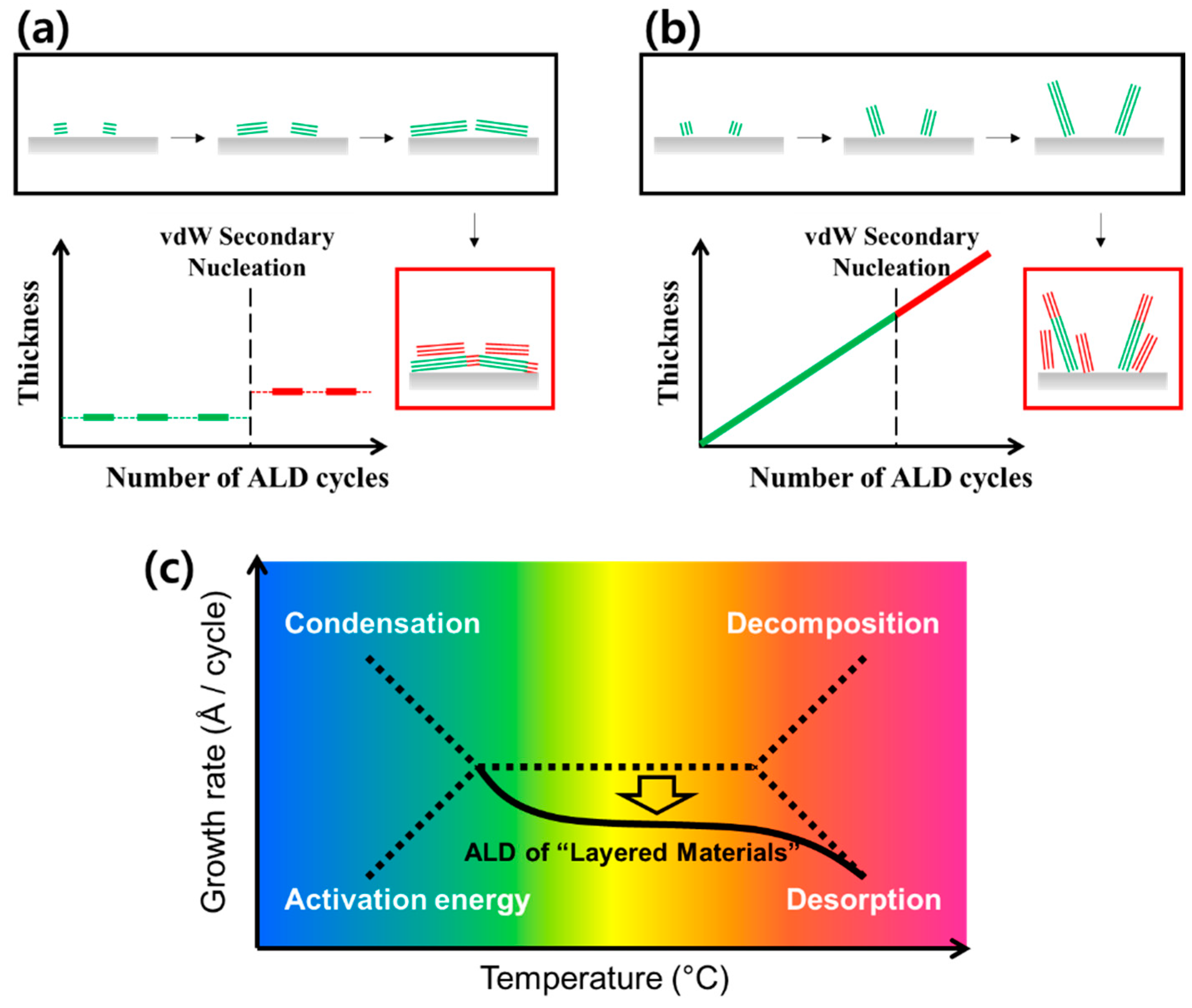
6.2. Growth Mechanisms of TM(D)C in ALD

ALD is advantageous because it provides (i) control over film thicknesses at the level of atomic layers, and (ii) the capability of conformal coating on many different substrates once the surface chemistries have been well established [108,109]. Considering the intrinsic limitations of Si photoelectrode, conformal surface coating with a thin layer and controlling charge transfer from Si to catalyst surface is highly desired. Therefore, the ALD strategy to the efficient energy transfer in PEC systems should be a powerful tool not only for coating functional materials such as metals, semiconductors, and insulators but also for incorporating dopant elements in a controlled fashion. Recently, along with the explosive interest in monolayer and few-layer TM(D)Cs, the synthesis of TM(D)C by the ALD processes has also received huge attention. Most ALD chemistries so far have been focused on amorphous and nanocrystalline materials where anisotropy in the crystalline structures was ignored. Moreover, the direct formation of crystalline MX2 by ALD is difficult and whether ALD operates well for layered materials has not yet been answered [110,111]. An important question was how the ALD of layered materials works if a directional component predominates over the others, or in other words, how to control anisotropic growth during ALD [76]. This would allow for a general understanding of ALD for layered materials. Figure 11 illustrates two distinctive growth modes of layered materials by ALD. Figure 11a highlights highly textured in-plane growth via van der Waals (vdW) attachments when growing layered materials by ALD. In contrast, Figure 12b represents a vertical growth mode where layer-by-layer growths along the basal plane with strong covalent bonding of MoS2 is common. Note that both are the result of the identical ALD chemistry where the ALD reactions contribute the crystal growth along the basal plane and the vdW secondary nucleation does not take place (see the upper row of Figure 11). However, each growth mode determines the final growth rate by which the mode operates, even though an identical chemistry is employed (see graphs of panels a and b). This understanding is distinctive when compared with the conventional ALD growths. By controlling the growth mode in the form of Figure 11a, therefore, the highly textured growth of TM(D)C materials is possible, and with appropriate single-crystal substrates, the epitaxial heterojunction growth of TM(D)C layers could be realized.

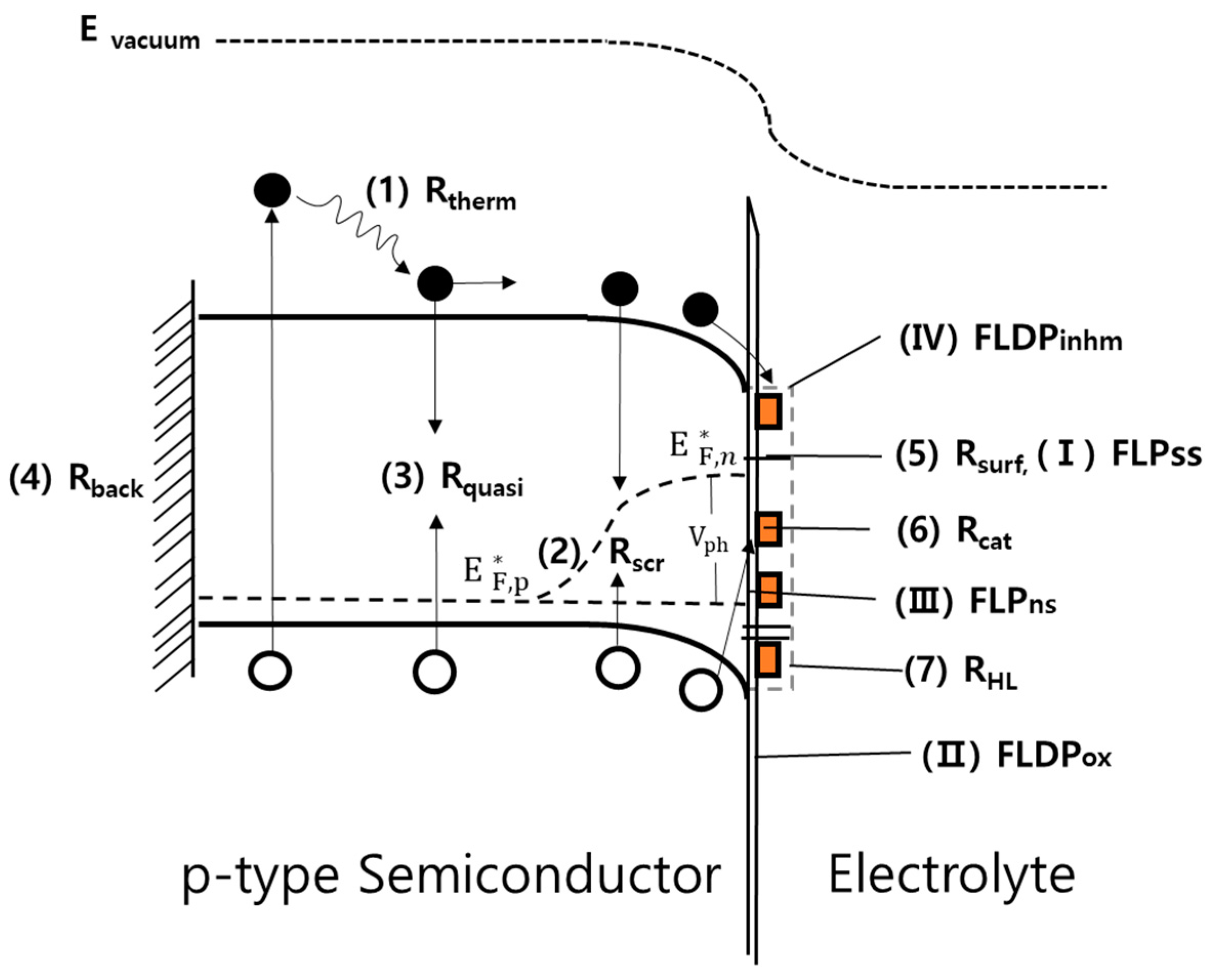
7. Measurement Tools for Understanding Operation Mechanisms

There are various measurement tools to analyze the efficiency and characteristics of PEC WS using semiconductors. It is important not only to measure flat-band potential or impedance, but also to analyze surfaces/heterojunctions formed with the different materials. In this section, Kelvin probe force microscopy (KPFM), ultraviolet photoelectron spectroscopy (UPS) and transient absorption spectroscopy (TAS) are introduced as tools for analyzing the roles of TM(D)C co-catalysts on Si photoelectrodes.

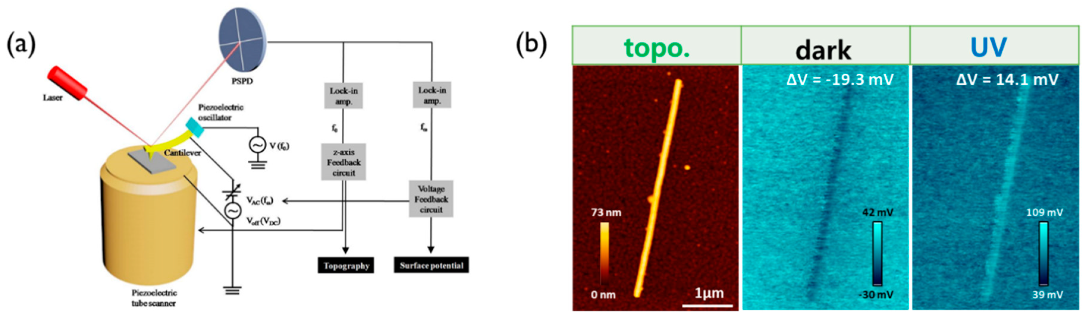
7.1. Kelvin Probe Force Microscopy (KPFM)

KPFM or Kelvin force microscopy (KFM) and spectroscopy (KPFS) are variants of atomic force microscopy (AFM) by using a Kelvin probe method and are capable of directly imaging the charge separation/transfer phenomena on the surfaces of the materials because of the nanometer scale spatial resolution and few mV sensitivity in the surface potential. From the vacuum level variation measurement at a material surface, KPFM is, therefore, suited to examine the band offsets (bending) of heterojunctions, especially 2D materials, as well as the mechanism of the photoinduced charge separation.
During KPFS measurement, the cantilever is approached on the sample and the mechanical vibration for the non-contact approach is stopped. The AC bias is applied between the tip and the sample to make the harmonic oscillation of the cantilever caused by an induced Coulombic force. Then, the voltage that minimizes the ω term (first-harmonic) of harmonic oscillation is measured as a contact potential difference (CPD) while sweeping the DC bias. CPD is described as follows:
C P D   ( V ) = Φ tip     Φ sample   q
where Φ tip is the work function of the cantilever, Φ sample is the work function of the sample, and q is the electron charge. If we simplify the interaction between the tip and the sample as a two-parallel-plate capacitor model, the total energy (U) can be expressed as follows,
U = 1 2 C Δ V 2
where C is the total capacitance and V is the applied bias between the two plates. If we simultaneously apply alternating current (AC) bias and direct current (DC) bias (V = VDC + VAC sin (ωt)) between the tip and the sample, the force is expressed as follows (Ref):
F = U z = 1 2 C Z V 2 = F d c + F ω + F 2 ω
F d c = 1 2 C z [ ( V d c Δ Φ ) 2 + V a c 2 2 ]
F ω = C z [ ( V d c Δ Φ ) V a c   sin ( ω t ) ]
F 2 ω = 1 4 C z [ ( V a c 2   cos ( 2 ω t ) ]
When the ω component of the force (Equation (11)) is zero, then VDC is equal to the work function difference between the tip and the sample. Therefore, one can measure the work function difference by sweeping the DC bias and calibration with the well-known standard sample to find the nullifying value of the first harmonic term.
It is also possible to study charge transfer and charge separation in a nanostructure via surface potential differences, ΔV = (VsampleVsubstrate)UV − (VsampleVsubstrate)dark, which are displayed by area-averaging each micrograph. Some results of investigating the characteristics of semiconductor and semiconductor/metal heterojunction used in a photoelectrode using KPFM are as follows. Yoo et al. measured the Schottky barrier height by mapping the co-catalyst-decorated oxide semiconductor junctions under ultraviolet (UV) light illumination [112]. Under UV illumination, the authors directly observed the charge separation phenomena at the Au-nanoparticle/TiO2-nanotube interfaces. They observed that in a steady state, approximately 0.3 of an electron per Au particle of approximately 4 nm in diameter is effectively charged and consequently screens the surface potential of the underlying TiO2 nanotubes (see Figure 13b). Polak et al. visualized the CPD after UV light illumination and confirmed the presence of a trap state using NaTaO3, which was utilized as the photoanode [113]. In a recent report, the measured surface potential of the photoanode BiVO4 and the heterojunction of BiVO4 with electrodeposited AgOx and NiOx is higher than BiVO4/AgOx and BiVO4/NiOx [114].
Almadori el al. measured the surface potential image of the WSe2/MoS2 van der Waals heterojunction using KPFM, from which the band alignment at the monolayer interface was obtained. They confirmed the impact of the defects to the photocarrier generation and the diffusion of negative charges near the heterojunction as well as the OCP value [115], by the surface photovoltage (SPV) image observation. Li et al. demonstrated the more efficient charge separation of photogenerated carriers in n-Si/MoS2 compared to that in p-Si/MoS2 by using KFM. The measured KFM results under dark and illumination condition also yielded the band alignment of Si/MoS2 heterojunctions and the separation of photogenerated excitons [116]. The analysis of the surface potential with photoassisted KPFM can also provide the information regarding the composition and electronic state of the local structures and the potential difference caused by the mixed-phase under illumination on the surface of a solid. Kim et al. conducted a KPFM measurement for two samples which are FeS2 thin films grown at 350 and 400 °C, respectively, to obtain the work function for each. FeS2 thin films grown at 350 °C showed multiple sharp work function peaks between 4.4 to 4.7 eV, meaning that several different phase, such as pyrrhotite phases and marcasite exist on the surface. The 400 °C-grown FeS2 thin film showed a smooth work function distribution, indicating that a single pyrite phase was developed [117].

7.2. Optical Spectroscopy

Ultraviolet photoelectron spectroscopy (UPS): UPS has long been used to identify the band structure of semiconductors. The operation principle of UPS is analyzing the ejected photoelectron energy when the photon energy of is irradiated on the surface. UPS normally utilizes a gas source of Helium, which has an energy of 21.21 eV (He I) or 40.82 eV (He II) with very narrow linewidths (≈20 meV). This energy is much lower than the source of X-ray photoelectron spectroscopy (XPS) and Auger electron spectroscopy (AES). The equation to calculate the ejected electron energy is similar to the XPS equation, Ekin = EB − ΦS. Due to low excitation energy in UPS, the binding energy (EB) cannot reach the core level, but to shallow valence band or adsorbates on the surface. With these characteristics, UPS has been employed to study the surface-associated band structure and interactions of gaseous molecules with surfaces. Not only to determine the band-edge levels of semiconducting absorbers but to study even cascade electrode having multiple interfaces of thin film and catalyst layers are possible. Chi et al. utilized UPS measurement to determine the energy level alignment of CdSe, CdS, and TiO2/CdS/CdSe electrodes to analyze the outperformance of TiO2/CdS/CdSe electrode [118]. They confirmed the stepwise energy level of the electrode and the conduction band minimum (CBM) position shift of the materials. Fingerle et al. made a schematic model interface model of nickel oxide/water to investigate the role of nickel oxide as an OER catalyst and water adsorption surface chemistry from the results of XPS core level and UPS valence band analysis [119] Wan et al. analyzed the Fermi level of SrNbO3 with a 1 wt % of platinum powder co-catalyst with UPS analysis [120]. Liu et al. used He I source (21.22 eV) UPS to determine the ionization potential (equivalent to the valence band energy) of C3N4 [121]. With the UPS analysis, important physical measures such as conduction band edge position or surface modified properties are efficiently estimated.
Transient absorption spectroscopy (TAS): in many photophysical and photochemical reactions, information regarding time-resolved carrier dynamics within nanoseconds or even picoseconds is critical. This becomes far more important for Si and TM(D)C heterojunction structures, and TAS is one of the most useful analytic tool to understand the charge transfer dynamics affected by the co-catalytic TM(D)C in PEC WS. TAS is well known pump-probe spectroscopy, which uses two extremely short pulses of light from a laser to excite (or pump) a molecule, and then probe it. The pulse of the pump pulse is tunable from the microsecond to the femtosecond, allowing us to excite materials of interest to a desired excited state. By varying the arrival time difference of the second pulse with respect to the first one, one can measure the entire time-dependence of the absorption changes. Nd:YAG, Ti-doped Sapphire and Yb:KGW are popular laser sources for TAS, with controlled wavelengths for the desired sample. This tool was first applied by Furube et al. for measuring the decay time of photogenerated carriers in K4Nb6O17 photocathode thin film [122]. Moss et al. used TAS with three polymorphs of TiO2 and identified the carrier recombination dynamics with a microsecond laser [123]. Wan et al. investigated the dynamic process of the hot electron in Pt/SrNbO3 with femtosecond time-resolved TAS [120].

8. Toward Multi-Phase TM(D)C Co-Catalysts on Si

The classic Volmer–Heyrovsky–Tafel mechanism on metal/electrolyte interfaces would explain HER activity. The hydronium ion reduction is, for example, described below:
(Volmer step) H3O+ + e + M ⇌ M-H + H2O
(Heyrovsky step) M-H + H3O+ + e ⇌ H2 + H2O + M
(Tafel step) 2M-H ⇌ H2 + M
With the Tafel reaction possessing the ideal surface coverage, one can obtain the theoretical kinetic description to be an ideal Tafel slope of ~30 mV/dec. The ideal or dense coverage pertains to the moderate binding energy on metal surfaces, producing the so-called the volcano plot. However, the presence of hydrogen bubbles on (co-)catalysts also hinders the diffusion of H+/H3O+ ions and the subsequent recombination by electrons. This may imply that dense layers of catalysts or co-catalysts are not necessary considering the (sub)micrometer-sized hydrogen gas bubbles at the stage of nucleation. Note that a very thin layer of electrolytes would exist between the bubble and the underlying catalyst, but the interdiffusion of electrolytes is also limited through it. Therefore, the multi-/mixed-phase co-catalysts could be ideal candidates of Si/TM(D)C for efficient HER, although they do not offer dense, and the best, catalytic surfaces in that (1) it can protect the whole area of the absorber surfaces, and (2) it can alter or optimize the surface energetics by laterally re-arranging the material properties.
Consequently, Figure 14 shows a research direction in the field toward employing multi-phase TM(D)C co-catalysts on Si for efficient PEC HER. Modifying the semiconductor surface with a metal of high work functions ( Φ w ) are ideal (Figure 14a). However, noble metals are not wetting directly to Si and a thin layer of adhesion promoter is required. This paradoxically involves a catalytically inactive interlayer on Si photocathodes (Figure 14b). Employing multi-phase TM(D)C co-catalysts on Si would be beneficial in maximizing PEC performance (Figure 14c). In case of metal oxide photocatalysts (for example, TiO2), there are several reports that the mixture phase helps charge transfer, resulting in effective charge separation and suppressing the charge recombination [124]. However, whether the same mechanism is applied to TMD materials or not in terms of composition and phase structure needs further studies. Interestingly, much research is underway on phase engineering of TMD materials, and papers regarding the facilitated charge transfer between heterophases within TMD homojunction have been published which are drawing attention. Kappera et al. demonstrated the locally induced 1T MoS2 phase on 2H phase in plane, showing improved sharp atomic interface between two phases which enhance the 2D electronic device performance [125]. Cho et al. achieved a stable heterophase homojunction in MoTe2 by laser-derived phase patterning [126]. The homojunction heterophase exhibits ohmic contact in MoTe2 transistors, implying that the charge transfer between the interphase in the TMD materials can be facilitated. The result was confirmed by measuring the Arrhenius plot showing the conductance of the heterophase homojunction channel. Ho et al. successfully grew a mixed-phase and continuous 1T and 2H homojunction MoS2 catalyst film on Si, via ALD at low temperature (250 °C) [76]. The conduction band energy relative to vacuum level of 2H phase of MoS2 and the work function of 1T phase are similar (~4.2 eV) [79] which secures band alignment, and in view of this, Joe et al. explained that mixed-phase MoS2/silicon junction photocathode showed effective photocatalytic performance through the efficient charge transfer within the MoS2 homojunction heterophase [53]. The ALD-grown MoS2 layer functions as a monolithic structure for effective charge transport within the film and was shown that the effective barrier height reached up to 0.8 eV with the optimized MoS2 thickness. The p-Si/MoS2 heterojunction photocathode was confirmed to show effective PEC operation characteristics due to the inhomogeneous barrier heights induced from the embedded 1T-phase within the film. This structural characteristic was introduced to boosts the electron transfer pathway effectively compared to a conventional MIS electrode via the embedded and metallic 1T phase, which increases the overall intrinsic property of the film.
As shown Figure 15a, Chen et al. showed that a CoMoSx composite display better electron accepting properties and HER catalytic activity compared with a-MoSx, proving that a bimetallic sulfide catalyst is highly efficient in extracting photogenerated electrons in reducing protons to hydrogen gas. The Si/a-CoMoSx hybrid photocathode showed onset potential of 0.25 V vs. RHE and photocurrent Isc of 17.5 mA cm−2 at 0 V vs. RHE in pH of 4.25. Zhang et al. enhanced the PEC performance significantly by decorating NiCoSex on p-Si nanopillars (Figure 15b). They proposed the possible reasons: (i) the effective light trapping capability of the nanopillars and the good optical transparency of NiCoSex; (ii) the full coverage of the electrochemically active NiCoSex material onto the pillars. In our previous work, Joe et al. demonstrated the energetically favorable path of photogenerated electrons from p-Si to electrolyte through the mixed-phase MoS2 catalyst layer and obtained the maximum 0.29 V onset voltage with the photocurrent density Jsc of 26.7 mAcm−2 at 0 V vs. RHE (Figure 15c). In addition to the examples listed above, studies demonstrating that mixed phases, along with multiphase, are more effective for charge separation and transfer and improve PEC performance continue to emerge.
To drive PEC WS effectively, three steps must be coherently operated as follows: (I) maximal photon absorption in the semiconductor; (II) exciton separation and the subsequent generation of mobile charges by minimal recombination; and (III) charge collection at opposite electrodes via good junction characteristics. The key recombination factors that prevent effective PEC WS are described in Figure 16. (1) Rtherm: photogenerated charge carriers that have excess energy due to absorb more solar energy than its band gap lose energy by thermalization. (2) Rscr: different concentration of charge form depletion region at the interface. The flowing charge is recombined until it is at equilibrium. (3) Rquasi: carriers passing the space charge region passing through the quasi-neutral region. If diffusion length of the carrier is shorter than can reach the back metal, recombination occurs at the quasi-neutral region. (4) Rback: recombination caused by ohmic contact which is formed between absorber and back contact metal. (5) Rsurf: lattice imperfection at the surface form energy state which called surface state. This energy state can be recombination center at the surface. (6) Rcat: the charge carrier travel through the catalyst layer can be recombined due to the delayed charge transfer process. (7) RHL: Voltage drop caused by the Helmholtz layer which generated when electrodes immersed in the electrolyte, typical voltage drop of HL is known as 0.1 to 0.5 V. Rtherm, Rback and Rquasi are intrinsic properties of bulk semiconductor (Si) which cannot control with catalyst, while the Rsurf and Rcat have room to be minimized via physical or chemically induced modification using the co-catalyst. Moreover, the overall performance of a PEC WS cell is determined by the voltage drop across the depletion region in contact with TM(D)C and/or within TM(D)C. How the separated and mobile charges are transferred effectively with minimum number of recombination is of paramount importance. Recent studies also report that multi-phase TM(D)C layers exhibit superior properties for HER although the exact origins were not clarified to date.
Here, we envision that employing continuous and multi-/mixed-phased metal chalcogenides on Si would be an ideal co-catalytic system in the application of PEC WS. We begin the discussion by highlighting our previous investigation on mixed-phase (1T and 2H) MoS2 on Si. The resulting metal and semiconducting homo-junctions have negligible barrier along the catalytic overlayers. Note that hetero-junctions of TM(D)C could also have similar barrier-lowering effects by band structure hybridization at the interfaces [127]. Therefore, it is important to understand how the deposited TM(D)C material (here, MoS2) on Si surface affects the charge recombination. In the literature [53,74,81], it was argued that depending on the thickness of the MoS2 catalyst layer, the Fermi-level pinning (FLPss) tends to be gradually relieved, possibly resulting in suppression of the Rsurf. The reduced Rsurf leads to increasing the Vph, results in reducing the Rscr and the Rquasi. Moreover, when using ALD method which enables one continuous and conformal coating, the layer-dependent properties can be better observed. This differs from using metals that are deposited in the form of an island. Indeed, Thorne et al. studied that in the PEC WS of hematite Fe2O3, the overlayer of NiFeOx, known as a co-catalyst led the slow surface hole transfer. However, it made the recombination rate slowed more at the interfaces, resulting in better water oxidation performance by intensity-modulated photocurrent spectroscopy [35]. Such a study implies that even in the co-catalytic systems, the pin-hole free surface overlayers should play a critical role in the efficient PEC WS.
Another consideration for the enhancement of PEC performance is Rcat derived from the film characteristics. Based on the examples demonstrated in Figure 15, we believe that in our previous paper, a number of secured electron pathways through 1T-MoS2 to 2H-MoS2 provide facilitate charge transfer within the catalyst film. We speculate that this might result in suppressing the recombination within the film and thus contributes to an improvement in the PEC performance. The MoS2 films with physical inhomogeneities in nanoscale dimensions smaller than the depletion width due to the coexistence of 1T and 2H phase form inhomogeneous junctions with the Si, accordingly.
What makes the continuous multi-/mixed-phased metal chalcogenides different is that the charge transfers take place at the whole interface areas. The inclusion of metallic (or degenerated) phases in the multi-/mixed-phased chalcogenides could form a nano-Schottky junction with Si. Thus, Fermi-level pinning (FLPnS) is expected by nanoscale junctions as a result of so-called ‘environmental Fermi-level pinning’ at around the Schottky junction interfaces [128]. Note also that there exists Fermi-level depinning (FLDPox) by the presence of oxide interfaces, e.g., SiOx between the metal and Si [129]. We also suspect that the presence of the continuously mixed phases would lead to ideal band edge pinning, indicative of facilitated charge transfer in the catalyst layer [53], reducing Rcat. Moreover, the catalysts with a lateral dimension less than the depletion width and with different work function values form inhomogeneous junctions to the absorber. These mechanisms were suspected to be offset from each other in the enhancement of Vph. The association of the physical inhomogeneous junction properties with Vph can be explained by the pinch-off effects, indicative of Fermi-level depinning (FLDPinhm) [130]. Together with stable interfaces by ALD and the multi-/mixed-phase overlayers, the ALD-grown TM(D)C/Si photocathodes should be capable of regulating the overall energy barriers and impedances of the total junctions and are expected for long-term operation in PEC WS.

9. Conclusions and Outlook

In summary, we have looked at the basic principles and the recent progress of Si-based photoelectrodes with TM(D)C co-catalysts as Earth-abundant candidates. Investigation of photoelectrodes using Si as one of the low band gap semiconductors and the mechanisms was also summarized with an emphasis on the exact role and the nature of catalysts. So far, TM(D)C materials are highly competitive Earth-abundant and inexpensive alternatives to noble metals due to the high durability in acid solution with catalytic activities. We provide an almost complete literature survey on both layered TMDC and non-layered TMC co-catalysts on Si photoelectrodes and different measurement tools for analyzing the effects of the TM (D) C catalyst on Si have been described. Various synthesis methods of TMD Catalysts and the corresponding performances were classified accordingly. Diverse approaches to the improved PEC performance and the proposed synergetic functions of co-catalysts on the underlying Si are reviewed. Among the various methods of depositing the catalyst, we focus on atomic layer deposition (ALD) which is prized for its conformal film deposition. Further on, the growth mechanism of TM(D)C material using ALD and its implication of low-temperature growth on defect chemistry are featured. We highlighted the multi-/mixed-phase TM(D)C overlayers on Si and the operation principles, and provided challenges and directions regarding future research for achieving the theoretical PEC performance of Si-based photoelectrodes. To support this, the band bending of the mixed-phase TM(D)C on Si and the related recombination mechanisms were discussed, which could provide a guideline for an efficient photoelectrode design to improve PEC performance. Despite the significant progress, the stable operation of photoelectrodes continues to be challenging which requires further improvement in optimizing the synthesis method as well as the overall system.

Author Contributions

Conceptualization, C.B. and H.S.; Methodology, J.J. and H.Y.; Writing-Original Draft Preparation, C.B., J.J. and H.Y.; Writing-Review and Editing, C.B. and H.S.; Supervision, C.B. and H.S.

Funding

The authors acknowledge the grants by the National Research Foundation of Korea (NRF-2018R1D1A1B07051059, NRF-2016M3D1A1027664, NRF-2018M3C1B7020716 and NRF-2018K1A3A1A32055268).

Conflicts of Interest

The authors declare no conflict of interest.

References

  1. Walter, M.G.; Warren, E.L.; McKone, J.R.; Boettcher, S.W.; Mi, Q.; Santori, E.A.; Lewis, N.S. Solar Water Splitting Cells. Chem. Rev. 2010, 110, 6446–6473. [Google Scholar] [CrossRef]
  2. Bocarsly, A.B.; Bookbinder, D.C.; Dominey, R.N.; Lewis, N.S.; Wrighton, M.S. Photoreduction at Illuminated p-Type Semiconducting Silicon Photoelectrodes. Evidence for Fermi Level Pinning. J. Am. Chem. Soc. 1980, 102, 3683–3688. [Google Scholar] [CrossRef]
  3. Chu, S.; Li, W.; Yan, Y.; Hamann, T.; Shih, I.; Wang, D.; Zetian, M. Roadmap on solar water splitting: Current status and future prospects. Nano Futures 2017, 1, 022001. [Google Scholar] [CrossRef]
  4. Kulkarni, A.; Siahrostami, S.; Patel, A.; Nørskov, J.K. Understanding Catalytic Activity Trends in the Oxygen Reduction Reaction. Chem. Rev. 2018, 118, 2302–2312. [Google Scholar] [CrossRef]
  5. Thorne, J.E.; Li, S.; Du, C.; Qin, G.; Wang, D. Energetics at the Surface of Photoelectrodes and Its Influence on the Photoelectrochemical Properties. J. Phys. Chem. Lett. 2015, 6, 4083–4088. [Google Scholar] [CrossRef]
  6. Zhong, D.K.; Choi, S.; Gamelin, D.R. Near-Complete Suppression of Surface Recombination in Solar Photoelectrolysis by Co-Pi Catalyst-Modified W: BiVO4. J. Am. Chem. Soc. 2011, 133, 18370–18377. [Google Scholar] [CrossRef]
  7. Hu, S.; Xiang, C.; Haussener, S.; Berger, D.A.; Lewis, N.S. An analysis of the optimal band gaps of light absorbers in integrated tandem photoelectrochemical water-splitting systems. Energy. Environ. Sci. 2013, 6, 2984–2993. [Google Scholar] [CrossRef]
  8. Abdi, F.F.; Han, L.; Smets, A.H.M.; Zeman, M.; Dam, B.; Van De Krol, R. Efficient solar water splitting by enhanced charge separation in a bismuth vanadate-silicon tandem photoelectrode. Nat. Commun. 2013, 4, 2195:1–2195:7. [Google Scholar] [CrossRef]
  9. Urbain, F.; Wilken, K.; Smirnov, V.; Astakhov, O.; Lambertz, A.; Becker, J.P.; Rau, Y.; Ziegler, J.; Kaiser, B.; Jaegermann, W.; et al. Development of Thin Film Amorphous Silicon Tandem Junction Based Photocathodes Providing High Open-Circuit Voltages for Hydrogen Production. Int. J. Photoenergy 2014, 249317:1–249317:10. [Google Scholar] [CrossRef]
  10. Benchamekh, R.; Nesoklon, M.; Jancu, J.-M.; Voisin, P. Semiconductor Modeling Techniques, 1st ed.; Springer: Berlin/Heidelberg, Germany, 2012; ISBN 978-3-642-43467-9. [Google Scholar]
  11. Wang, S.; Tian, H.; Ren, C.; Yu, J.; Sun, M. Electronic and optical properties of heterostructures based on transition metal dichalcogenides and graphene-like zinc oxide. Sci. Rep. 2018, 8, 12009. [Google Scholar] [CrossRef]
  12. Pfluger, E.; Savan, A. Modern Solid Lubricants, Especially Based on MoS2. Vak. Forsch. Prax. 1999, 11, 236–240. [Google Scholar] [CrossRef]
  13. Bae, C.; Böhnert, T.; Gooth, J.; Lim, S.; Lee, S.; Kim, H.; Heimann, S.; Schulz, S.; Shin, H.; Nielsch, K. Thermopower Engineering of Bi2Te3 without Alloying: The interplay between nanostructuring and defect activation. Semicond. Sci. Technol. 2014, 29, 064003. [Google Scholar] [CrossRef]
  14. Yang, E.; Ji, H.; Jung, Y. Two-Dimensional Transition Metal Dichalcogenide Monolayers as Promising Sodium Ion Battery Anodes. J. Phys. Chem. C 2015, 119, 26374–26380. [Google Scholar] [CrossRef]
  15. Gu, X.; Cui, W.; Li, H.; Wu, Z.; Zeng, Z.; Lee, S.-T.; Zhang, H.; Sun, B. A Solution-Processed Hole Extraction Layer Made from Ultrathin MoS2 Nanosheets for Efficient Organic Solar Cells. Adv. Energy. Mater. 2013, 3, 1262–1268. [Google Scholar] [CrossRef]
  16. Chhowalla, M.; Shin, H.S.; Eda, G.; Li, L.J.; Loh, K.P.; Zhang, H. The chemistry of two-dimensional layered transition metal dichalcogenide nanosheets. Nat. Chem. 2013, 5, 263–275. [Google Scholar] [CrossRef]
  17. Guio, C.G.M.; Stern, L.A.; Hu, X. Nanostructured hydrotreating catalysts for electrochemical hydrogen evolution. Chem. Soc. Rev. 2014, 43, 6555–6569. [Google Scholar] [CrossRef]
  18. Van de Krol, R. Principles of Photoelectrochemical Cells, 1st ed.; Springer: Boston, MA, USA, 2011; ISSN 978-1-4614-1380-6. [Google Scholar]
  19. Rasmussen, A.F.; Thygesen, S.K. Computational 2D Materials Database: Electronic Structure of Transition-Metal Dichalcogenides and Oxides. J. Phys. Chem. C 2015, 119, 13169–13183. [Google Scholar] [CrossRef]
  20. Lu, Q.; Yu, Y.; Ma, Q.; Chen, B.; Zhang, H. 2D Transition-Metal-Dichalcogenide-Nanosheet-Based Composites for Photocatalytic and Electrocatalytic Hydrogen Evolution Reactions. Adv. Mater. 2016, 28, 1917–1933. [Google Scholar] [CrossRef]
  21. Galicia-Hernandez, J.M.; Sanchez-Castillo, A.; Garza, L.M.; Cocoletzi, H.G. Two-dimensional cadmium selenide electronic and optical properties: First principles studies. Bull. Mater. Sci. 2017, 40, 1111–1119. [Google Scholar] [CrossRef]
  22. Tamirat, A.G.; Rick, J.; Dubale, A.A.; Sub, W.N.; Hwang, B.J. Using hematite for photoelectrochemical water splitting: A review of current progress and challenges. Nanoscale Horiz. 2016, 1, 243–267. [Google Scholar] [CrossRef]
  23. Mak, F.; Lee, C.; Hone, J.; Shan, J.; Heinz, F. Atomically Thin MoS2: A New Direct Gap Semiconductor. Phys. Rev. Lett. 2010, 105, 136805:1–136805:4. [Google Scholar] [CrossRef]
  24. Simon, T.; Bouchonville, N.; Berr, M.; Vaneski, A.; Adrovic, A.; Volbers, D.; Wyrwich, R.; Doblinger, M.; Susha, A.; Rogach, A.; et al. Redox shuttle mechanism enhances photocatalytic H2 generation on Ni-decorated CdS nanorods. Nat. Mater. 2014, 13, 1013–1018. [Google Scholar] [CrossRef]
  25. Wiensch, J.D.; John, J.; Velazquez, J.M.; Torelli, D.A.; Pieterick, A.P.; McDowell, M.T.; Sun, K.; Zhao, X.; Brunschwig, B.S.; Lewis, N.S. Comparative Study in Acidic and Alkaline Media of the Effects of pH and Crystallinity on the Hydrogen-Evolution Reaction on MoS2 and MoSe2. ACS Energy Lett. 2017, 2, 2234–2238. [Google Scholar] [CrossRef]
  26. Memming, R. Semiconductor Electrochemistry, 2nd ed.; Wiley: New York, NY, USA, 2000; ISBN 978-3-527-31281-8. [Google Scholar]
  27. Lewis, N.S. A Quantitative Investigation of the Open-Circuit Photovoltage at the Semiconductor/Liquid Interface. J. Electrochem. Soc. 1984, 131, 2496–2503. [Google Scholar] [CrossRef]
  28. Baglio, J.A.; Calabrese, G.S.; Harrion, D.J.; Kamieniecki, E.; Ricco, A.J.; Wrighton, M.S.; Zoski, G.D. Electrochemical characterization of p-type semiconducting tungsten disulfide photocathodes: Efficient photoreduction processes at semiconductor/liquid electrolyte interfaces. J. Am. Chem. Soc. 1983, 105, 2246–2256. [Google Scholar] [CrossRef]
  29. Markovic, N.M.; Grgur, B.N.; Ross, R.N. Temperature-Dependent Hydrogen Electrochemistry on Platinum Low-Index Single-Crystal Surfaces in Acid Solutions. J. Phys. Chem. B 1997, 101, 5405–5413. [Google Scholar] [CrossRef]
  30. Yang, J.; Wang, D.; Han, H.; Li, C. Roles of Cocatalysts in Photocatalysis and Photoelectrocatalysis. Acc. Chem. Res. 2013, 46, 1900–1909. [Google Scholar] [CrossRef] [Green Version]
  31. Reichman, J. The current-voltage characteristic of semiconductor-electrolyte junction photovoltaic cells. J. Appl. Phys. Lett. 1980, 36, 574–576. [Google Scholar] [CrossRef]
  32. Gartner, W.W. Depletion-Layer photoeffects in Semiconductors. Phys. Rev. 1959, 116, 84–87. [Google Scholar] [CrossRef]
  33. Peng, K.Q.; Wang, X.; Wu, X.L.; Lee, S.T. Platinum Nanoparticle Decorated Silicon Nanowires for Efficient Solar Energy Conversion. Nano Lett. 2009, 9, 3704–3709. [Google Scholar] [CrossRef]
  34. Bao, N.Z.; Shen, L.M.; Takata, T.; Domen, K. Self-Templated Synthesis of Nanoporous CdS nanostructures for Highly Efficient Photocatalytic Hydrogen Production under Visible Light. Chem. Mater. 2008, 20, 110–117. [Google Scholar] [CrossRef]
  35. Thorne, J.E.; Jang, J.W.; Liu, E.Y.; Wang, D. Understanding the origin of photoelectrode performance enhancement by probing surface kinetics. Chem. Sci. 2016, 7, 3347–3354. [Google Scholar] [CrossRef] [Green Version]
  36. Upadhyay, R.K.; Soinb, N.; Roy, S.S. Role of graphene/metal oxide composites as photocatalysts, adsorbents and disinfectants in water treatment: A review. RSC Adv. 2014, 4, 3823–3851. [Google Scholar] [CrossRef]
  37. Li, H.; Hu, H.; Bao, C.; Guo, F.; Zhang, X.; Liu, X.; Hua, J.; Tan, J.; Wang, A.; Zhou, H.; et al. Forming heterojuction: An effective strategy to enhance the photocatalytic efficiency of a new metal-free organic photocatalyst for water splitting. Sci. Rep. 2016, 6, 29327. [Google Scholar] [CrossRef] [PubMed]
  38. Sivula, K.; Van De Krol, R. Semiconducting materials for photoelectrochemical energy conversion. Nat. Rev. Mater. 2016, 1, 15010. [Google Scholar] [CrossRef] [Green Version]
  39. White, J.R.; Fan, F.R.F.; Bard, A. Semiconductor Electrodes LVI. Principles of Multijunction Electrodes and Photoelectrosynthesis at Texas Instruments’p/n-Si Solar Arrays. J. Electrochem. Soc. 1985, 132, 544–550. [Google Scholar] [CrossRef]
  40. Delahoy, A.E.; Gau, S.C.; Murphy, O.J.; Kapur, M.; JO’M, B. A one-unit photovoltaic electrolysis system based on a triple stack of amorphous silicon (pin) cells. Int. J. Hydrog. Energy 1985, 10, 113–116. [Google Scholar] [CrossRef]
  41. Kronik, L.; Shapira, Y. Surface photovoltage phenomena: Theory, experiment, and applications. Surf. Sci. Rep. 1999, 37, 1–206. [Google Scholar] [CrossRef]
  42. Han, L.; Digdaya, I.A.; Buijs, T.W.; Abdi, F.F.; Huang, Z.; Liu, R.; Dam, B.; Zeman, M.; Smith, W.A.; Smets, A.H. Gradient dopant profiling and spectral utilization of monolithic thin-film silicon photoelectrochemical tandem devices for solar water splitting. J. Mater. Chem. A 2015, 3, 4155–4162. [Google Scholar] [CrossRef] [Green Version]
  43. Sabba, D.; Kumar, M.H.; Wong, L.H.; Barber, J.; Grätzel, M.; Mathews, N. Perovskite–Hematite Tandem Cells for Efficient Overall Solar Driven Water Splitting. Nano Lett. 2015, 15, 3833–3839. [Google Scholar]
  44. Li, F.; Fan, K.; Xu, B.; Gabrielsson, E.; Daniel, Q.; Li, L.; Sun, L. Organic Dye-Sensitized Tandem Photoelectrochemical Cell for Light Driven Total Water Splitting. J. Am. Chem. Soc. 2015, 137, 9153–9159. [Google Scholar] [CrossRef] [PubMed]
  45. Chen, Z.; Dinh, H.N.; Miller, E. Photoelectrochemical Water Splitting standards, Experimental Methods, and Protocol, 1st ed.; Springer: New York, NY, USA, 2013; pp. 63–103. [Google Scholar]
  46. Dos Santos, W.S.; Rodriguez, M.; Afonso, A.S.; Mesquita, J.P.; Nascimento, L.L.; Patrocínio, A.O.T.; Silva, A.C.; Oliveira, L.C.A.; Fabris, J.D.; Pereira, M.C. A hole inversion layer at the BiVO4/Bi4V2O11 interface produces a high tunable photovoltage for water splitting. Sci. Rep. 2016, 4, 31406. [Google Scholar] [CrossRef] [PubMed]
  47. Deutsch, T.G.; Koval, C.A.; Turner, J.A. III-V Nitride Epilayers for Photoelectrochemical Water Splitting: GaPN and GaAs PN. J. Phys. Chem. B 2006, 110, 25297–25307. [Google Scholar] [CrossRef] [PubMed]
  48. Koster, L.J.A.; Mihailetchi, V.D.; Ramaker, R.; Blom, P.W.M. Light Intensity dependence of open-circuit voltage of polymer-fullerene solar cells. Appl. Phys. Lett. 2005, 86, 123509. [Google Scholar] [CrossRef]
  49. Kumar, P.; Jain, S.C.; Kumar, H.; Chand, S.; Kumar, V. Effect of illumination intensity and temperature on open circuit voltage in organic solar cells. Appl. Phys. Lett. 2009, 94, 183505. [Google Scholar] [CrossRef] [Green Version]
  50. Chegaar, M.; Hamzaoui, A.; Namoda, A.; Petit, P.; Aillerie, M.; Herguth, A. Effect of illumination intensity on solar cells parameters. Energy Procedia 2013, 36, 722–729. [Google Scholar] [CrossRef]
  51. Yu, X.; Sivula, K. Photogenerated Charge Harvesting and Recombination in Photocathodes of Solvent-Exfoliated WSe2. Chem. Mater. 2017, 29, 6863–6875. [Google Scholar] [CrossRef]
  52. Liu, B.; Li, X.-B.; Gao, Y.-J.; Li, Z.-J.; Meng, Q.-Y.; Tung, C.-H.; Wu, L.Z. A solution-processed, mercaptoacetic acid-engineered CdSe quantum dot photocathode for efficient hydrogen production under visible light irradiation. Energy. Envorn. Sci. 2015, 8, 1443–1449. [Google Scholar] [CrossRef]
  53. Joe, J.; Bae, C.; Kim, E.; Ho, T.A.; Yang, H.; Park, J.H.; Shin, H. Mixed-Phase (2H and 1T) MoS2 Catalyst for a Highly Efficient and Stable Si Photocathode. Catalysts 2018, 8, 580. [Google Scholar] [CrossRef]
  54. Kornienko, N.; Gibson, N.A.; Zhang, H.; Eaton, S.W.; Yu, Y.; Aloni, S.; Leone, S.R.; Yang, P. Growth and Photoelectrochemical Energy Conversion of Wurtzite Indium Phosphide nanowire Arrays. ACS Nano 2016, 10, 5525–5535. [Google Scholar] [CrossRef]
  55. Digdaya, I.A.; Han, L.; Buijs, T.W.F.; Zeman, M.; Dam, B.; Smets, A.H.M.; Smith, W.A. Extracting large photovoltages from a-SiC photocathodes with an amorphous TiO2 front surface field layer for solar hydrogen evolution. Energy Environ. Sci. 2015, 8, 1585–1593. [Google Scholar] [CrossRef]
  56. Liu, C.; Wang, F.; Zhang, J.; Wang, K.; Qiu, Y.; Liang, Q.; Chen, Z. Efficient Photoelectrochemical Water Splitting by g-C3N4/TiO2 Nanotube Array Heterostructures. Nano-Micro Lett. 2018, 10, 37. [Google Scholar] [CrossRef]
  57. Digdaya, I.A.; Adhyaksa, G.W.P.; Trzes´niewski, B.J.; Garnett, E.C.; Smith, W.A. Interfacial engineering of metal-insulator-semiconductor junctions for efficient and stable photoelectrochemical water oxidation. Nat. Commun. 2017, 8, 15968. [Google Scholar] [CrossRef] [PubMed] [Green Version]
  58. Ye, L.; Wang, D.; Chen, S. Fabrication and Enhanced Photoelectrochemical Performance of MoS2/S-Doped g-C3N4 Heterojunction Film. ACS Appl. Mater. Interfaces 2016, 8, 5280–5289. [Google Scholar] [CrossRef] [PubMed]
  59. Tewary, V.k.; Jain, S.C. Open-Circuit Voltage Decay in Solar cells. Adv. Electron. Phys. 1986, 67, 319–414. [Google Scholar]
  60. Wang, Q. Fast Voltage Decay in Perovskite Solar Cells Caused by Depolarization of Perovskite Layer. J. Phys. Chem. C 2018, 122, 4822–4827. [Google Scholar] [CrossRef]
  61. Sekizawa, K.; Oh-ishi, K.; Kataoka, K.; Arai, T.; Suzuki, T.M.; Morikawa, T. Stoichiometric water splitting using a p-type Fe2O3 based photocathode with the aid of a multiheterojunction. J. Mater. Chem. A 2017, 5, 6483–6493. [Google Scholar] [CrossRef]
  62. Bisquert, J.; Zaban, A.; Greenshtein, M.; Mora-Sero, I. Determination of Rate Constants for Charge Transfer and the Distribution of Semiconductor and Electrolyte Electronic Energy Levels in Dye-Sensitized Solar Cells by Open-Circuit Photovoltage Decay Method. J. Am. Chem. Soc. 2004, 126, 13550–13559. [Google Scholar] [CrossRef] [PubMed]
  63. Su, J.Z.; Guo, L.; Bao, N.Z.; Grimes, C.A. Nanostructured WO3/BiVO4 Heterojunction Films for Efficient Photoelectrochemical Water Splitting. Nano Lett. 2011, 11, 1928–1933. [Google Scholar] [CrossRef] [PubMed]
  64. Yu, X.; Du, R.; Li, B.; Zhang, Y.; Liu, H.; Qu, J.; An, X. Biomolecule-assisted self-assembly of CdS/MoS2/graphene hollow spheres as high-efficiency photocatalysts for hydrogen evolution without noble metals. Appl. Catal. B Environ. 2016, 182, 504–512. [Google Scholar] [CrossRef]
  65. Yang, Y.; Xu, D.; Wu, Q.Y.; Diao, P. Cu2O/CuO Bilayered Composite as a High-Efficiency Photocathode for Photoelectrochemical Hydrogen Evolution Reaction. Sci. Rep. 2016, 6, 35158. [Google Scholar] [CrossRef] [PubMed]
  66. Hill, J.C.; Landers, A.T.; Switzer, J.A. An electrodeposited inhomogeneous metal-insulator-semiconductor junction for efficient photoelectrochemical water oxidation. Nat. Mater. 2015, 14, 1150–1155. [Google Scholar] [CrossRef] [PubMed]
  67. Pawar, G.S.; Tahir, A.A. Unbiased Spontaneous Solar Fuel Production using Stable LaFeO3 Photoelectrode. Sci. Rep. 2018, 8, 3501:1–3501:9. [Google Scholar] [CrossRef]
  68. Hu, D.; Xiang, J.; Zhou, Q.; Su, S.; Zhang, Z.; Wang, X.; Jin, M.; Nian, L.; Nözel, R.; Zhou, G.; et al. One-step chemical vapor deposition of MoS2 noanosheet on SiNWs as photocathodes for efficint and stable solar-driven hydrogen production. Nanoscale 2018, 10, 3518–3525. [Google Scholar] [CrossRef]
  69. Zhou, J.; Dai, S.; Dong, W.; Su, X.; Fang, L.; Zheng, F.; Wang, X.; Shen, M. Efficient and stable MoS2 catalyst integrated on Si photocathodes by photoreduction and post-annealing for water splitting. Appl. Phys. Lett. 2016, 108, 213905. [Google Scholar] [CrossRef]
  70. Devarapalli, R.R.; Kamaja, C.K.; Shelke, M.V. Quantum dot-decorated silicon nanowires as efficient photoelectrodes for photoelectrochemical hydrogen generation. J. Mater. Chem. A 2014, 2, 133352–133358. [Google Scholar] [CrossRef]
  71. Lopes, T.; Andrade, L.; Formal, F.L.; Gratzel, M.; Sivula, K.; Mendes, A. Hematite photoelectrodes for water splitting: Evaluation of the role of film thickness by impedance spectroscopy. Phys. Chem. Chem. Phys. 2014, 16, 16515–16523. [Google Scholar]
  72. Lopes, T.; Andrade, L.; Ribeiro, H.A.; Medes, A. Characterization of photoelectrochemical cells for water splitting by electrochemical impedance spectroscopy. Int. J. Hydrog. Energy 2010, 23, 11601–11608. [Google Scholar] [CrossRef]
  73. Fujishima, A.; Honda, K. Electrochemical photolysis of water at a semiconductor electrode. Nature 1972, 238, 37–38. [Google Scholar] [CrossRef]
  74. Andoshe, M.D.; Jin, G.; Lee, C.; Kim, C.; Kwon, K.C.; Choi, S.; Sohn, W.; Moon, C.W.; Lee, S.H.; Suh, J.M.; et al. Directly Assembled 3D Molybdenum Disulfide on Silicon Wafer for Efficient Photoelectrochemical Water Reduction. Adv. Sustain. Syst. 2018, 2, 1700142. [Google Scholar] [CrossRef]
  75. Ding, Q.; Meng, F.; English, C.R.; Acevedo, M.C.; Shearer, M.J.; Liang, D.; Daniel, A.S.; Hamers, R.J.; Jin, S. Efficient photoelectrochemical Hydrogen Generation Using Heterostructures of Si an Chemically Exfoliated Metallic MoS2. J. Am. Chem. Soc. 2014, 136, 8504–8507. [Google Scholar] [CrossRef] [PubMed]
  76. Ho, T.A.; Bae, C.; Lee, S.; Kim, M.; Montero-Moreno, J.M.; Park, J.H.; Shin, H. Edge-On MoS2 Thin Films by Atomic Layer Deposition for Understanding the Interplay between the Active Area and Hydrogen Evolution Reaction. Chem. Mater. 2017, 29, 7604–7614. [Google Scholar] [CrossRef]
  77. Fan, R.; Mao, J.; Yin, Z.; Jie, J.; Dong, W.; Fang, L.; Zheng, F.; Shen, M. Efficient and Stable Silicon Photocathodes Coated with Vertically Standing Nano-MoS2 Films for Solar Hydrogen Production. ACS Appl. Mater. Interfaces 2017, 9, 6123–6129. [Google Scholar] [CrossRef] [PubMed]
  78. Oh, S.; Kim, J.B.; Song, J.T.; Oh, J.H.; Kim, S.H. Atomic layer deposited molybdenum disulfide on Si photocathodes for highly efficient photoelectrochemical water reduction reaction. J. Mater. Chem. A 2017, 5, 3304–3310. [Google Scholar] [CrossRef]
  79. Du, P.; Zhu, Y.; Zhang, J.; Xu, D.; Peng, W.; Zhang, G.; Zhang, F.; Fan, X. Metallic 1T phase MoS2 nanosheets as a highly efficient co-catalyst for the photocatalytic hydrogen evolution of CdS nanorods. RSC Adv. 2016, 6, 74394–74399. [Google Scholar] [CrossRef]
  80. Kwon, K.C.; Choi, S.; Hong, K.; Moon, C.W.; Shim, Y.-S.; Kim, D.H.; Kim, T.; Sohn, W.; Jeon, J.-M.; Lee, C.H.; et al. Wafer-scale transferable molybdenum disulphide thin-film catalyst for photoelectrochemical hydrogen production. Energy Environ. Sci. 2016, 9, 2240–2248. [Google Scholar] [CrossRef]
  81. Fujii, K.; Ono, M.; Iwaki, Y.; Sato, K.; Ohkawa, K.; Yao, T. Photoelectrochemical Properties of the p−n Junction in and near the Surface Depletion Region of n-Type GaN. J. Phys. Chem. C 2010, 114, 22727–22735. [Google Scholar] [CrossRef]
  82. Tran, D.P.; Pramana, S.S.; Kale, S.V.; Nguyen, M.; Chiam, T.S.; Batabyal, K.S.; Wong, H.L.; Barber, J.; Loo, J. Novel Assembly of an MoS2 Electrocatalyst onto a Silicon Nanowire Array Electrode to Construct a Photocathode Composed of Elements Abundant on the Earth for Hydrogen Generation. Chem. Eur. J. 2012, 18, 13994–13999. [Google Scholar] [CrossRef]
  83. Zhou, Q.; Su, S.; Hu, D.; Lin, L.; Yan, Z.; Gao, X.; Zhang, Z.; Liu, J. Ultrathin MoS2-coated Ag@Si nanosphere arrays as an efficient and stable photocathode for solar-driven hydrogen production. Nanotechnology 2018, 29, 105402–105410. [Google Scholar] [CrossRef]
  84. Zeng, L.; Liu, Y.; Lin, S.; Qarony, W.; Tao, L.; Chai, Y.; Zhang, X.; Lau, P.S.; Tsang, H.Y. High photoelectrochemical activity and stability of Au-WS2/silicon heterojunction photocathode. Sol. Energy Mater. Sol. Cells 2018, 174, 300–306. [Google Scholar] [CrossRef]
  85. Benck, D.J.; Lee, S.; Fong, D.K.; Kibsgaard, J.; Sinclair, R.; Jaramillo, F.T. Designing Active and Stable Silicon Photocathodes for Solar Hydrogen Production Using Molybdenum Sulfide Nanomaterials. Adv. Energy. Mater. 2014, 4, 1400739. [Google Scholar] [CrossRef]
  86. King, L.A.; Hellstern, T.R.; Park, J.; Sinclair, R.; Jaramillo, T.F. Highly Stable Molybdenum Disulfide Protected Silicon Photocathodes for Photoelectrochemical Water Splitting. ACS Appl. Mater. Interfaces 2017, 9, 36792–36798. [Google Scholar] [CrossRef] [PubMed]
  87. Huang, G.; Mao, J.; Fan, R.; Yin, Z.; Wu, X.; Jie, J.; Kang, Z.; Shen, M. Integrated MoSe2 with n+p-Si photocathodes for solar water splitting with high efficiency and stability. Appl. Phys. Lett. 2018, 112, 013902. [Google Scholar] [CrossRef]
  88. Zhang, L.; Liu, C.; Wong, B.A.; Resasco, J.; Yang, P. MoS2-wrapped silicon nanowires for photoelectrochemical water reduction. Nano Res. 2015, 8, 281–287. [Google Scholar] [CrossRef]
  89. Chandra, G.; Roy, M.A.; Bhattacharya, S.S. Effect of n-Si on the Photocatalytic Production of Hydrogen by Pt-loaded CdS and CdS/ZnS Catalyst. Int. J. Hydrog. Energy 1996, 21, 19–23. [Google Scholar] [CrossRef]
  90. Hou, T.; Abrams, L.B.; Vesborg, C.K.P.; Bjorketun, E.M.; Herbst, K.; Bech, L.; Setti, M.A.; Damsgaard, D.C.; Pedersen, T.; Hansen, O.; et al. Bioinspired molecular co-catalysts bonded to a silicon photocathode for solar hydrogen evolution. Nat. Mater. 2011, 10, 434–438. [Google Scholar] [CrossRef] [PubMed] [Green Version]
  91. Hou, Y.; Zhu, Z.; Xu, Y.; Guo, F.; Zhang, J.; Wang, X. Efficient photoelectrochemical hydrogen production over p-Si nanowire arrays coupled with molybdenume-sulfur clusters. Int. J. Hydrog. Energy 2017, 42, 2832–2838. [Google Scholar] [CrossRef]
  92. Huang, Z.; Wang, C.; Pan, L.; Tian, F.; Zhang, X.; Zhang, C. Enhanced photoelectrochemical hydrogen production using silicon nanowires@MoS3. Nano Energy 2013, 2, 1337–1346. [Google Scholar] [CrossRef]
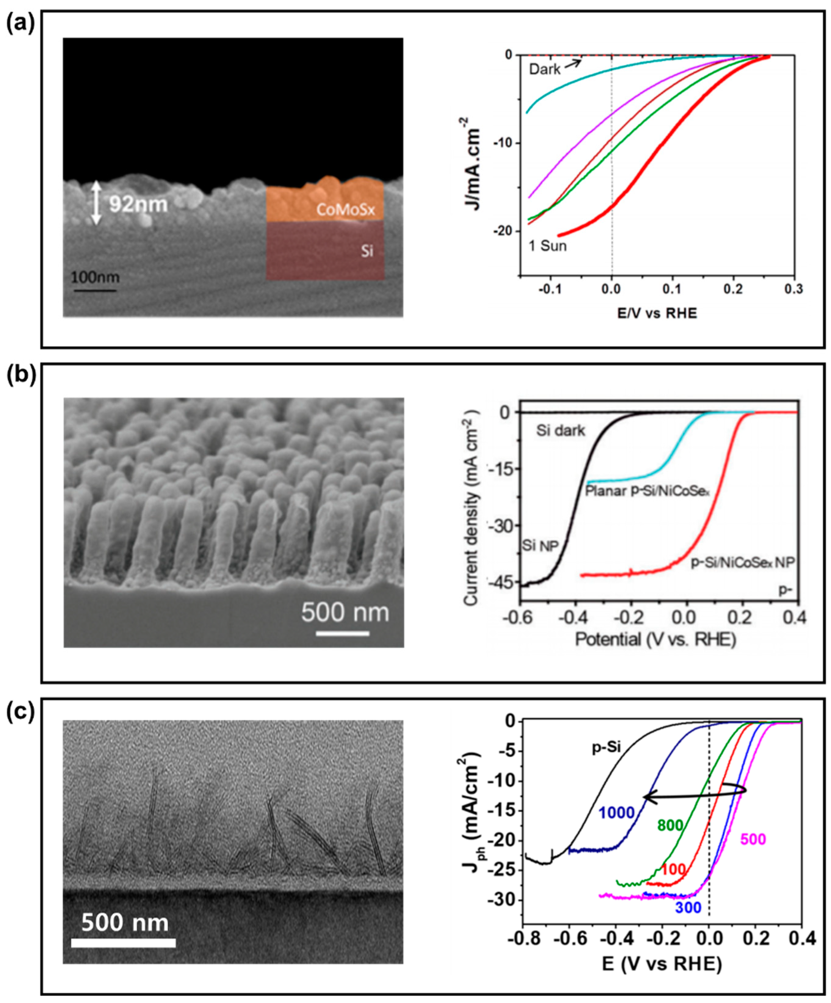
  93. Zhang, H.; Ding, Q.; He, D.; Liu, H.; Liu, W.; Li, Z.; Yang, B.; Zhang, X.; Lei, L.; Jin, S. A p-Si/NiCoSex core/shell nanopillar array photocathode for enhanced photoelectrochemical hydrogen production. Energy Environ. Sci. 2016, 9, 3113–3119. [Google Scholar] [CrossRef]
  94. Chen, Y.; Tran, P.; Boix, P.; Ren, Y.; Chiam, Y.S.; Li, Z.; Fu, K.; Wong, H.L.; Barber, J. Silicon Decorated with Amorphous Cobalt Molybdenum Sulfide Catalyst as an Efficient Photocathode for Solar Hydrogen Generation. ACS Nano 2015, 9, 3829–3836. [Google Scholar] [CrossRef]
  95. Chen, C.; Chen, P.; Basu, M.; Yang, K.; Lu, Y.; Dong, C.; Ma, C.; Shen, C.; Hu, S.; Liu, R. An integrated cobalt disulfide (CoS2) co-catalyst passivation layer on silicon microwires for photoelectrochemical hydrogen evolution. J. Mater. Chem. A 2015, 3, 23466–23476. [Google Scholar] [CrossRef]
  96. Chen, C.; Yang, K.; Basu, M.; Lu, T.; Lu, Y.; Dong, C.; Hu, S.; Liu, R. Wide Range pH-Tolerable Silicon@Pyrite Cobalt Dichalcogenide Microwire Array Photoelectrodes for Solar Hydrogen Evolution. ACS Appl. Mater. Interfaces 2016, 8, 5400–5407. [Google Scholar] [CrossRef] [PubMed]
  97. Basu, M.; Zhang, Z.; Chen, C.; Chen, P.; Yang, K.; Ma, C.; Lin, C.; Hu, S.; Liu, R. Heterostructure of Si and CoSe2: A Promising Photocathode Based on a Non-noble Metal Catalyst for Photoelectrochemical Hydrogen Evolution. Angew. Chem. Int. Ed. 2015, 54, 6211–6216. [Google Scholar] [CrossRef] [PubMed]
  98. Bazri, B.; Lin, Y.; Lu, T.; Chen, C.; Kowsari, E.; Hu, S.; Liu, R. A heteroelectrode structure for solar water splitting: Integrated cobalt ditelluride across a TiO2-passivated silicon microwire array. Catal. Sci. Technol. 2017, 7, 1488–1496. [Google Scholar] [CrossRef]
  99. Seger, B.; Laursen, B.A.; Vesborg, C.K.P.; Pedersen, T.; Hansen, O.; Dahl, S.; Chorkendorff, I. Hydrogen Production Using a Molybdenum Sulfide Catalyst on a Titanium-Protected n+p-Silicon Photocathode. Angew. Chem. Int. Ed. 2012, 51, 9128–9131. [Google Scholar] [CrossRef] [PubMed]
  100. Yadian, B.; Rao, Y.; Zhu, B.; Liu, Z.; Liu, Q.; Gan, L.C.; Chen, X.; Huang, Y. Metal-sulfide-decorated ZnO/Si nano-heterostructure arrays with enhanced photoelectrochemical performance. Mater. Res. Bull. 2017, 96, 503–508. [Google Scholar] [CrossRef]
  101. Nie, X.; Zhuo, S.; Maeng, G.; Sohlberg, K. Doping of TiO2 Polymorphs for Altered Optical and Photocatalytic Properties. Int. J. Photoenergy 2009, 294042:1–294042:22. [Google Scholar]
  102. Morgan, B.; Watson, G. Intrinsic n-type Defect Formation in TiO2: A Comparison of Rutile and Anatase from GGA+U Calculations. J. Phys. Chem. C 2010, 114, 2321–2328. [Google Scholar] [CrossRef]
  103. Fahey, P.; Griffin, P.; Plummer, J. Point defects and dopant diffusion in silicon. Rev. Mod. Phys. 1989, 61, 289–384. [Google Scholar] [CrossRef]
  104. Scanlon, D.; King, P.; Singh, R.; Torre, A.; Walker, S.; Balakrishnan, G.; Baumberger, F.; Catlow, C. Controlling Bulk Conductivity in Topological Insulators: Key Role of Anti-Site Defects. Adv. Mater. 2012, 24, 2154–2158. [Google Scholar] [CrossRef]
  105. Fuschillo, N.; Bierly, N.J.; Donahoe, F.J. Transport properties of the pseudo-binary alloy system Bi2Te3−ySey. J. Phys. Chem. Solids 1959, 8, 430–433. [Google Scholar] [CrossRef]
  106. Miller, G.R.; Li, C. Evidence for the existence of antistructure defects in bismuth telluride by density measurements. J. Phys. Chem. Solids 1965, 26, 173–177. [Google Scholar] [CrossRef]
  107. Ghoshtagore, R.N. Self-Diffusion in Tellurium. I. Anisotropy and Impurity Effect. Phys. Rev. 1967, 155, 598–602. [Google Scholar] [CrossRef]
  108. George, S.M. Atomic Layer Deposition: An Overview. Chem. Rev. 2010, 110, 111–131. [Google Scholar] [CrossRef]
  109. Kim, H.; Lee, H.B.R.; Maeng, W.J. Applications of atomic layer deposition to nanofabrication and emerging nanodevices. Thin Solid Films 2009, 517, 2563–2580. [Google Scholar] [CrossRef]
  110. Jin, Z.; Shin, S.; Kwon, D.H.; Han, S.J.; Min, Y.S. Novel chemical route for atomic layer deposition of MoS2 thin film on SiO2/Si substrate. Nanoscale 2014, 6, 14453–14458. [Google Scholar] [CrossRef]
  111. Song, J.G.; Ryu, G.H.; Lee, S.J.; Sim, S.; Lee, C.W.; Choi, T.; Jung, H.; Kim, Y.; Lee, Z.; Myoung, J.M.; et al. Controllable synthesis of molybdenum tungsten disulfide alloy for vertically composition-controlled multilayer. Nat. Commun. 2015, 6, 7817. [Google Scholar] [CrossRef] [PubMed] [Green Version]
  112. Yoo, H.; Bae, C.; Yang, Y.; Lee, S.; Kim, M.; Kim, H.; Kim, Y.; Shin, H. Spatial Charge Separation in Asymmetric Structure of Au Nanoparticle on TiO2 Nanotube by Light-Induced Surface Potential Imaging. Nano Lett. 2014, 14, 4413–4417. [Google Scholar] [CrossRef] [PubMed]
  113. Polak, L.; Rector, J.; Slaman, M.; Wijngaarden, R. NaTaO3 Photoanode for Bias-Free Water Splitting: A Photo-Electrochemical and Kelvin Probe Surface Photovoltage Study. J. Phys. Chem. C 2016, 120, 23559–23565. [Google Scholar] [CrossRef]
  114. Hu, Y.; Wu, Y.; Feng, J.; Huang, H.; Zhang, C.; Qian, Q.; Fang, T.; Xu, J.; Wang, P.; Li, Z.; et al. Rational design of electrocatalysts for simultaneously promoting bulk charge separation and surface charge transfer in solar water splitting photoelectrodes. J. Mater. Chem. A 2018, 6, 2568–2576. [Google Scholar] [CrossRef]
  115. Almadori, Y.; Bendiab, N.; Grévin, B. Multimodal Kelvin Prove Force Microscopy Investigations of a Photovoltaic WSe2/MoS2 Type-ll interface. ACS Appl. Mater. Interfaces 2018, 10, 1363–1373. [Google Scholar] [CrossRef] [PubMed]
  116. Li, Y.; Xu, C.-Y.; Wang, J.-Y.; Zhen, L. Photodiode-Like Behavior and Excellent Photoresponse of Vertical Si/Monolyer MoS2 Heterostructures. Sci. Rep. 2014, 4, 7186:1–7186:8. [Google Scholar]
  117. Kim, J.; Kim, G.Y.; Moon, H.; Yoon, S.; Seo, I.W.; Lee, Y.; Moon, D.G.; Ahn, S.J.; Jo, W. Identification of marcasite in pyrite FeS2 fhim films and the films’ carrier transport characeristics. RSC Adv. 2016, 6, 81394–81399. [Google Scholar] [CrossRef]
  118. Chi, C.F.; Cho, H.W.; Teng, H.; Chuang, C.Y.; Chang, Y.M.; Hsu, Y.J.; Lee, Y.L. Energy level alignment, electron injection, and charge recombination characteristics in CdS/CdSe cosensitized TiO2 photoelectrode. Appl. Phys. Lett. 2011, 98, 012101. [Google Scholar] [CrossRef]
  119. Fingerle, M.; Tengeler, S.; Calvet, W.; Mayer, T.; Jaegermann, W. Water Interaction with Sputter-Deposited Nickel Oxide on n-Si Photoanode: Cryo Photoelectron Spectroscopy on Adsorbed Water in the Frozen Electrolyte Approach. J. Electrochem. Soc. 2018, 165, H3148–H3153. [Google Scholar] [CrossRef] [Green Version]
  120. Wan, D.; Zhao, Y.; Cai, Y.; Asmara, T.; Huang, Z.; Chen, J.; Hong, J.; Yin, S.; Nelson, C.; Motapothula, M.; et al. Electron transport and visible light absorption in a plasmonic photocatalyst based on strontium niobite. Nat. Commun. 2017, 8, 15070. [Google Scholar] [CrossRef] [PubMed]
  121. Liu, J.; Liu, Y.; Liu, N.; Han, Y.; Zhang, X.; Huang, H.; Lifshitz, Y.; Lee, S.; Zhong, J.; Kang, Z. Metal-free efficient photocatalyst for stable visible water splitting via a two-electron pathway. Science 2015, 347, 970–974. [Google Scholar] [CrossRef] [PubMed]
  122. Furube, A.; Shiozawa, T.; Ishikawa, A.; Wada, A.; Domen, K.; Hirose, C. Femtosecond Transient Absorption Spectroscopy on Photocatalysts: K4Nb6O17 and Ru(bpy)3 2+-Intercalated K4Nb6O17 Thin Films. J. Phys. Chem. B 2002, 106, 3065–3072. [Google Scholar] [CrossRef]
  123. Moss, B.; Lim, K.; Beltram, A.; Moniz, S.; Tang, J.; Fornasiero, P.; Barnes, P.; Durrant, J.; Kafizas, A. Comparing photoelectrochemical water oxidation, recombination kinetics and charge trapping in the three polymorphs of TiO2. Sci. Rep. 2017, 8, 2938:1–2938:7. [Google Scholar] [CrossRef] [PubMed]
  124. Liu, J.; Dai, M.; Wu, J.; Hu, Y.; Zhang, Q.; Cui, J.; Wang, Y.; Tan, H.H.; Wu, Y. Electrochemical hydrogenation of mixed-phase TiO2 nanotube arrays enables remarkably enhanced photoelectrochemical water splitting performance. Sci. Bull. 2018, 63, 194–202. [Google Scholar] [CrossRef]
  125. Kappera, R.; Voiry, D.; Yalcin, S.E.; Branch, B.; Gupta, G.; Mohite, A.D.; Chhowalla, M. Phase-engineered low-resistance contacts for ultrathin MoS2 transistors. Nat. Mater. 2014, 13, 1128–1134. [Google Scholar] [CrossRef]
  126. Cho, S.; Kim, S.; Kim, J.H.; Zhao, J.; Seok, J.; Keum, D.H.; Baik, J.; Choe, D.-H.; Chang, K.J.; Suenaga, K.; et al. Phase patterning for ohmic homojunction contact in MoTe2. Science 2015, 349, 625–628. [Google Scholar] [CrossRef]
  127. Li, M.Y.; Shi, Y.; Cheng, C.C.; Lu, L.S.; Lin, Y.C.; Tang, H.L.; Tsai, M.L.; Chu, C.W.; Wei, K.H.; He, J.H.; et al. Epitaxial growth of a monolayer WSe2-MoS2 lateral p-n junction with an atomically sharp interface. Science 2015, 349, 524–528. [Google Scholar] [CrossRef]
  128. Agrawal, A.; Lin, J.; Barth, M.; White, R.; Zheng, B.; Chopra, S.; Gupta, S.; Wang, K.; Gelatos, J.; Mohney, S.E.; et al. Fermi level depinning and contact resistivity reduction using a reduced titania interlayer in n-silicon metal-insulator-semiconductor ohmic contactsn nanowire array electrode to construct a photocathode composed of elements abundant on the earth for hydrogen generation. Appl. Phys. Lett. 2014, 104, 112101–112105. [Google Scholar]
  129. Smit, G.D.J.; Rogge, S.; Klapwijk, T.M. Scaling of nano-Schottky-diodes. Appl. Phys. Lett. 2002, 81, 3852–3854. [Google Scholar] [CrossRef] [Green Version]
  130. Rossi, R.C.; Lewis, N.S. Investigation of the Size-Scaling Behavior of Spatially Nonuniform Barrier Height Contacts to Semiconductor Surfaces Using Ordered Nanometer-Scale Nickel Arrays on Silicon Electrodes. J. Phys. Chem. B 2001, 105, 12303–12318. [Google Scholar] [CrossRef]
Figure 1. (a) Bandgaps and band edge positions of group IV, III-V semiconductors (green) and transition metal chalcogenides semiconductors (orange) relative to the hydrogen evolution reaction (HER) and oxygen evolution reaction (OER) active potentials (bulk band gaps corresponding to each are indicated in the dotted line below). (b) Solar irradiance spectrum of air mass (AM) 1.5 G for a 37° tilted surface. The ratio of absorbed solar light irradiance is integrated and is shown on the right-side y-axis of the graph (the blue line represents the irradiance unit of wavelength under 1 sun, and the black line represents the accumulated solar irradiance starting wavelength of 280 nm).
Catalysts 09 00149 g001
Figure 2. pH dependence of the band edge positions in an aqueous electrolyte solution. H+/H2 and O2/H2O potentials follow the Nernstian relation, which has a variation of 0.059 V/pH at 25 °C at 1 atm. Conversely, the slope of the semiconductor band edge position (red dotted line) according to pH could be different from that of water (green and yellow dotted line).
Catalysts 09 00149 g002
Figure 3. (a) A semiconductor photoanode/electrolyte junction under illumination showing the mechanism of photoelectrochemical (PEC) performance. EF,P* and EF,n* denote the quasi-Fermi level of Si for the hole and electron under illumination; Eox and Ered indicate the energy levels of a redox couple in the electrolyte. (b) Surface recombination of the electron-hole pair induced by the surface states of the semiconductor (i.e., Femi level pinning).
Catalysts 09 00149 g003
Figure 4. Energy diagram showing the roles of catalysts on Si in PEC performance. (a) Surface passivation of the semiconductor to reduce surface recombination. (b) Metal–semiconductor (MS) junction to enhance the electric field within the depletion region. Φ ph denotes the barrier height of Schottky junction. (c) Energy diagram for photocatalytic water splitting. ΔGo denotes the energy required for the uphill reaction.
Catalysts 09 00149 g004
Figure 5. Examples of silicon-based PEC half-cell configurations under illumination. (a) n-type Si photoanode, (b) p-type Si photocathode. (c) Photoanode with a catalyst layer on the surface, metal/n-Si (metal–semiconductor, MS) junction. (d) Photocathode with a catalyst layer on the surface, metal/p-Si (MS) junction. (e) p-n junction photoanode combined with a catalyst layer. (f) p-n junction photocathode combined with a catalyst layer. Two depletion layers exist in a sample at the junctions.
Catalysts 09 00149 g005
Figure 6. (a) Dark equilibrium condition of the n-type Si photoanode immersed in an electrolyte. The Fermi level is aligned with the redox potential of the electrolyte. (b) Photovoltage induced under illumination by creating quasi-Fermi level. (c) Flat-band potential (Vfb) is the potential at which the band bending flattens under sufficiently intense illumination.
Catalysts 09 00149 g006
Figure 7. Open-circuit potential (OCP) of different type of solar cells vs illumination intensity: photoelectrode of GaAsPN (3.6%N) 3M H2SO4 (V vs. Ag/AgCl) [47], MDMO-PPV: PCMB solar cell device [48], DSSC solar cell (ITO/CuPc/C60/BPen/Al) [49], polycrystalline Si [50].
Catalysts 09 00149 g007
Figure 8. The comparison graphs of open-circuit potential (OCP) difference measurements redrawn based on the Vph value from the references [5,51,52,53,54,55,56,57,58]. Different type of photocathodes (positive transition) and photoanodes (negative transition) under dark equilibrium and under illumination are shown.
Catalysts 09 00149 g008
Figure 9. Mott–Schottky plots from various photoelectrodes: (ac) photocathodes, and (df) photo anodes. (a) is adapted from reference [54]. Copyright (2016) American Chemical Society. (b) is adapted from reference [55] with permission from The Royal Society of Chemistry. (c) is adapted from reference [53]. (d) is adapted from reference [58]. Copyright (2016) American Chemical Society. (e) is adapted from reference [57]. (f) is adapted from reference [64] Republished with permission of Elsevier, from Biomolecule-assisted self-assembly of CdS/MoS2/graphene hollow spheres as high-efficiency photocatalysts for hydrogen evolution without noble metals, Yu et al., 182, 2016; permission conveyed through Copyright Clearance Center, Inc.
Catalysts 09 00149 g009
Figure 10. (a) A Nyquist plot for electrochemical cell covering regions of mass-transfer limitations (diffusion, Warburg) and kinetic (from kinetics of the electrochemical reaction, charge-transfer resistance). (b) The corresponding equivalent circuit representing the plot (a). (c) An energy diagram of a semiconductor photocathode/electrolyte interface with the corresponding electrical equivalent circuit.
Catalysts 09 00149 g010
Figure 11. Electrical and thermoelectric characterization of Bi2Te3 thin films grown at different Tsub. (a) The electrical conductivity, σ. (b) The Seebeck coefficient, S. Adapted from reference [13].
Catalysts 09 00149 g011
Figure 12. (a,b) Two distinctive growth modes of layered materials, such as MoS2 grown by atomic layer deposition (ALD). (c) Plot of the so-called “ALD window” with four factors affecting the nonideality of the ALD processes (i.e., condensation, decomposition, activation energy, and desorption). An incomplete reaction occurs because the activation energy for the reaction is not reached; adsorbed precursors on the surface react with the next precursor and remove the residue. However, there is not enough heat energy due to low chamber temperature so residues cannot be removed and remain as condensation; high temperature decomposes the precursor even before absorbing on the surface, and causes CVD-like deposition; the deposited compounds are desorbed because of excessive heat energy in the chamber). This plot revisits the ALD process of layered materials by adding an additional factor, i.e., strong structural anisotropy (see solid black line). Adapted from reference [76]. Copyright (2017) American Chemical Society.
Catalysts 09 00149 g012
Figure 13. (a) Operation mechanism of Kelvin probe force microscopy (KPFM). (b) The representative surface potential images of an Au/TNT on a Pt substrate before and after ultraviolet (UV) illumination. Adapted from reference [112]. Copyright (2014) American Chemical Society.
Catalysts 09 00149 g013
Figure 14. Developments of silicon photocathode with (a) co-catalysts, (b) adhesive junctions/co-catalysts, and (c) overlayers of multi-/mixed-phase chalcogenides.
Catalysts 09 00149 g014
Figure 15. Experimental reports on multi-/mixed-phase TM(D)C co-catalysts on silicon. (a) Cross-section view taken by scanning electron microscope (SEM) (left) and characterizations of the Si/a-CoMoSx electrode with a catalyst loading (right), the PEC current density (J) verses voltage (V) plots. Adapted from reference [94]. Copyright (2015) American Chemical Society. (b) SEM image of p-Si/NiCoSex nanoparticle (NP) array-nanopillars (left) and the corresponding PEC current density verses potential plots (right). Adapted from reference. [93] with permission from The Royal Society of Chemistry. (c) Cross-section transmission electron microscope (TEM) image of Mixed-phase (1T and 2H) MoS2 on p-Si photocathode(left) and the corresponding J-V characteristics with different thickness of MoS2 layer(right) the number of ALD cycle for MoS2 deposition is denoted in different color. Adapted from reference [53].
Catalysts 09 00149 g015
Figure 16. Basic recombination factors in PEC cells under illumination and the related effects. (1) Rthermo is the thermalization loss of the excited electron, (2) Rscr is the recombination of the space charge region (SCR) (depletion layer) at the surface, (3) Rquasi is the recombination at the quasi-neutral region of the semiconductor, (4) Rback is the back Ohmic contact recombination, (5) Rsurf is the surface recombination induced from the surface states of Si. (6) Rcat is the recombination occur within the MoS2 film. (7) RHL is Helmholtz layer recombination in the electrolyte. (I) FLPss is the Fermi-level pinning induced from the surface states, (II) FLDPox is the Fermi-level depinning due to the oxide (typically native oxide), (III) FLPns is the Fermi-level pinning induced from the nano Schottky junctions, (IV) FLDPinhm is the Fermi-level depinning results from the inhomogeneous Schottky junctions.
Catalysts 09 00149 g016
Table 1. Summary of the literature papers on the heterostructures of Si/TM(D)Cs for application in PEC water splitting (WS). Analyzed from Refs. [53,68,69,70,74,75,77,78,81,82,83,84,85,86,87,88,89,90,91,92,93,94,95,96,97,98,99,100].
PEC ProcessCell TypeConfigurationMX2 CompoundExperimental ConditionCurrent Density
(mAcm−2)
Onset Potential
(V vs RHE)
Light Source
(mWcm−2)
Stability (min)Ref.
TMDCPhotocathodeTMDC/SiMoS2/p-SiMoS20.5 M H2SO4 (pH = 0.3)/SCE Ref./Pt plate Counter24.6 (0V vs RHE)+0.17Xe Lamp
(100)
1666.7
(10000s)
[81]
MoS2/p-Si0.5 M H2SO4 (pH = 0.3)/Ag/AgCl/1 M KCl Ref./Graphite rod Counter17.6 (0V vs RHE)+0.231 sun
(100)
180[75]
MoS2/p-Si0.5 M H2SO4 (pH = 0.3)/Ag/AgCl/3M KCl Ref./Pt wire Counter21.7 (0V vs RHE)+0.231 sun
(100)
1440[78]
MoS2/p-Si NW1.0 M Na2SO4 buffer (pH = 5.0)/Not available1 (0V vs RHE)+0.25Xe Lamp
(100)
60[82]
0.5 M H2SO4 (pH = 0.3)/Ag/AgCl Ref./Pt wire Counter16.5 (0V vs RHE)+0.26Xe Lamp
(100)
2880[68]
MoS2/Ag@Si NS0.5 M H2SO4 (pH = 0.3)/Ag/AgCl Ref./Pt wire Counter33.3 (Saturated)+0.111 sun
(100)
720[83]
p-Si/SiOx/MoS20.5 M H2SO4 (pH = 0.3)/Ag/AgCl Ref./Pt wire Counter30(Saturated)+0.35Xe Lamp
(100)
4320[53]
Au/WS2/SiWS20.5 M H2SO4 (pH = 0.3)/Ag/AgCl Ref. Pt Counter0.37 (-1.0V vs RHE)Not AvailableNot Available50[84]
TMDC/
n+p-Si
MoS2/MoxSi Mo/n+p SiMoS20.5 M H2SO4 (pH = 0.3)/Hg/Hg2SO4 in saturated K2SO4 Ref./Ir Counter17 (0V vs RHE)+0.321 sun
(100)
6000[85]
MoS2/MoxSi
Mo/n+pSi
0.5 M H2SO4 (pH = 0.3)/Hg/Hg2SO4 in saturated K2SO4 Ref./Ir Counter19 (0V vs RHE)+0.2836360
(606h)
[86]
MoSe2/n+p-SiMoSe21.0 M HClO4 (pH = 1.0)/Ag/AgCl/3M KCl Ref./Pt Counter29.3 (Saturated)+0.40Xe Lamp
(100)
7200[87]
TMDC/Interlayer/
Si
MoS2/ALD TiO2/p-Si NWMoS20.5 M H2SO4 (pH = 0.3)/Ag/AgCl/1M NaCl Ref.15 (0V vs RHE)+0.301 sun
(100)
75[88]
3D MoS2/TiO2/p-Si0.5 M H2SO4 (pH = 0.3)/SCE Ref./Graphite Counter28 (0V vs RHE)+0.35Xe Lamp
(100)
6000[74]
TMDC/Interlayer/n+p-SiMoS2/Al2O3
n+p-Si
MoS21.0 M HClO4 (pH = 1.0)/Ag/AgCl/3M KCl Ref./Pt wire Counter35.6 (Saturated)+0.401 sun
(100)
7200[77]
TMCPhotocathodeTMC/SiCdS, ZnS/
n-Si powder
CdS, ZnS0.24 M Na2S + 0.35 M Na2SO3 (pH = 11.5)/Not AvailableNot Available (7.23mL/gh)Not Available(25)Not Available[89]
Mo3S4 cluster/Si NPMo3S41.0 M HClO4 (pH = 1.0)/Hg/HgSO4 Ref./Pt mesh Counter9 (0V vs RHE)+0.15Xe Lamp
(28.3)
60[90]
MoSx/P-SiMoSx0.5 M H2SO4 (pH = 0.3)/SCE Ref./Pt mesh Counter14.3 (0V vs RHE)+0.25Xe Lamp
(27.3)
180[91]
a-NiCoSex/
p-Si NP
NiCoSex0.5 M H2SO4 (pH = 0.3)/SCE Ref./Pt wire Counter37.5 (0V vs RHE)+0.251 sun
(100)
120[93]
a-CoMoSx/SiCoMoSxPhosphate (pH = 4.25)/Ag/AgCl/3M KCl Ref./Pt wire Counter17.5 vs (0.25V vs RHE)0.25Xe Lamp
(100)
180[94]
CdSe QD/
n-Si NW
CdSe0.25 M Na2S + 0.35 M Na2SO3 (pH = 11.5)/Hg/HgO Ref./
Pt foil Counter
6.1 (1.0V vs RHE)Not Available1 sun
(100)
< 1[70]
CoS2/p-Si MWCoS20.5 M H2SO4 (pH = 0.3)/Ag/AgCl Ref./Pt plate Counter3.22 (0V vs RHE)0.249Xe Lamp
(100)
180[94]
CoS2, CoSe2/p-Si MWCoS2, CoSe20.5 M H2SO4 (pH = 0.3)/Ag/AgCl Ref./Pt plate Counter3.22 (CoS2), 2.55 (CoSe2)0.248 (CoS2)
0.137 (CoSe2)
Xe Lamp
(100)
Not Available[96]
CoSex/Si MWCoSex0.5 M Na2SO4 (pH =1)/Ag/AgCl Ref./Pt foil Counter9 (-0.14V vs RHE)0.18Xe Lamp
(100)
50 cycles[97]
TMC/Interlayer/SiCoTex/ALD - TiO2/Si MWCoTex0.5 M H2SO4 (pH = 0.3)/0.5M Ag/AgCl Ref./Pt foil Counter24.0 (Saturated)0.17Xe Lamp
(100)
66.7
(4000s)
[98]
TMC/Interlayer/n+p SiMoSx/Ti-TiOx/n+p-SiMoSx1.0 M HClO4 (pH = 1.0)/Hg/HgSO4 Ref./Pt mesh Counter12 (0.2V vs RHE)+0.20(38.6)60[99]
a-MoS2/Al2O3/n+p-SiMoS21.0 M HClO4 (pH = 1.0)/Ag/AgCl Ref./Pt wire Counter34.5 (Saturated)+0.35Xe Lamp
(100)
2400[69]
PhotoanodeTMC/Interlayer/SiAg2S NP/ZnS/ZnO/p-Si NCAg2S, ZnS0.2 M Na2SO4 + PBS (pH = 7.25)/Ag/AgCl Ref./Pt foil Counter0.0588 vs (2.1V vs RHE)Not AvailableNot AvailableNot Available[100]
Table 2. Various synthesis routes of TM(D)Cs on Si photoelectrode.
MethodsCompoundsSpecific ProcessesRef.
CVDMoS2MoS2: (NH4)2MoS4 + H2 at 500 °C ~ 950 °C
MoS2: Mo (MoCl5, MoO3) + S (Sulfur powder) from 475 °C to 730 °C
[68,74,75,81,83]
SputteringMoSe2, WS2MoSe2: MoSe2 target Sputtering (400 °C, 50 W)
WS2: target Sputtering
[84,87]
Photo-electrodepositionMoS2, NiCoSeMoS2: (NH4)2[MoS4]/(NH4)2MoS4 + NaClO4
NiCoSex: NiCl + CoCl + SeO2
[77,82,89,93]
ALD (PLD)MoS2MoS2: 200 °C PLD, Mo(CO)6 + H2S, annealing in 500 ~ 700 °C H2S condition[53,78]
HydrothermalWS2, MoSx,
CoSex, ZnS
MoSx: (NH4)6Mo7O24·4H2O + ammonium polysulfide (96 °C, 120 h)
CoSex: EDTA + CoCl2·6H2O + Se Powder + NaOH (180 °C, 18 h)
ZnS2: 0.2 M thioacetamide +ZnNO3 (90 °C)
[91,96,97,100]
Drop-castingMo3S4, CoTe2Mo3S4: methylcyclopentadienyl ligands
CoTe2: Co(NO3)2·6H2O + Na2TeO4 in methanol
[90,92,98]
Electrodepositiona-MoS2, a-CoMoSa-MoS2: (NH4)2MoS4 + NaClO4/(NH4)2MoS4 + DMF
a-CoMoS: 0.25 mM [Co(MoS4)2]2-
[69,94,99]
SILARCdSeCdSe: Cd(NO3)2 +NaHSe + NaBH4 + SeO2[70]
Thermal SulfidationMoS2, CoS2, CoSe2MoS2: Mo Sputtering/Sulfidize (250 °C, H2S gas, 1 h)
CoS2: Co(OH)2 + Sulfur powder (500 °C, 1 h)
CoSe2: Co(NO)3·6(H2O) + S, Se powder
[85,86,95]
ThermolysisMoS2MoS2: (NH4)2MoS4 (573–673 K, N2/H2)[88]

