Article

SnSx (x = 1, 2) Nanocrystals as Effective Catalysts for Photoelectrochemical Water Splitting

1
Department of Materials Science and Engineering, National Cheng Kung University, Tainan 701, Taiwan
2
Department of Mechanical Engineering, Southern Taiwan University of Science and Technology, Tainan 710, Taiwan
3
Department of Chemical and Materials Engineering, National University of Kaohsiung, Kaohsiung 81148, Taiwan
4
Center for Micro/Nano Science and Technology, National Cheng Kung University, Tainan 70101, Taiwan
*
Author to whom correspondence should be addressed.
Catalysts 2017, 7(9), 252; https://doi.org/10.3390/catal7090252
Submission received: 1 August 2017 / Revised: 21 August 2017 / Accepted: 24 August 2017 / Published: 25 August 2017
(This article belongs to the Special Issue Advances in Electrocatalysis)

Abstract

:
Two-dimensional SnSx (x = 1, 2) nanocrystals are attractive catalysts for photoelectrochemical water splitting as their components are earth abundant and environmentally friendly. We have fabricated SnS thin-film photoelectrodes by spin coating mixed-phase SnS nanocrystals synthesized via a hot-injection technique on glass/Cr/Au substrates. The obtained SnS thin films can be transformed into SnS2 by introducing structural phase changes via a facile low-vacuum annealing protocol in the presence of sulfur. This sulfurization process enables the insertion of sulfur atoms between layers of SnS and results in the generation of shallow donors that alter the mechanism for water splitting. The SnS2 thin films are used as stable photocatalysts to drive the oxygen evolution reaction, and the light-current density of 0.195 mA/cm2 at 0.8 V vs. Ag/AgCl can be achieved due to the high carrier density, lower charge transfer resistance, and a suitable reaction band position. Based on a combination of UV-Vis spectroscopy (ultraviolet and visible spectroscopy), cyclic voltammetry and Mott–Schottky analysis, the band positions and band gaps of SnS and SnS2 relative to the electrolyte are determined and a detailed mechanism for water splitting is presented. Our results demonstrate the potential of layered tin sulfide compounds as promising photocatalysts for efficient and large-scale water splitting.

Graphical Abstract

1. Introduction

Photoelectrochemical (PEC) water splitting using semiconductor photoelectrodes, also referred to as artificial photosynthesis, is being widely pursued as an efficient approach for capturing and storing solar energy [1,2,3]. This technique can be traced back to the pioneering work of Honda and Fujishima [4], who used the band gap excitation of rutile TiO2 in a PEC cell with Pt as counter electrode (CE) and an applied bias to split water into molecular hydrogen and oxygen. Since then, much effort has been devoted to exploring new materials, altering synthesis protocols and engineering surfaces of existing materials to create active sites in order to enhance the production of H2/O2. Water splitting is a combination of both hydrogen and oxygen evolution reaction (HER and OER, respectively), and requires 237 kJ/mol of energy, which is equivalent to 1.23 eV. Therefore, the band gap of a workable photocatalyst should be greater than 1.23 eV to achieve water splitting, but less than 3 eV to ensure efficient utilization of visible light, where most solar irradiance is concentrated [1]. Semiconductor photocatalysts are considered as promising candidates for water splitting as they can generate electron–hole pairs under solar irradiation that can then trigger HER/OER. Although much research has been done to develop semiconductor photocatalysts, large band gaps (3.2 eV for TiO2), photocorrosion (CdS, Ta3N5) and unsuitable band positions (WO3, Fe2O3) are some of the issues that need to be addressed [1]. Furthermore, a good photocatalyst must be efficient, economical, stable, environmentally friendly and nontoxic.
Recently, two-dimensional layered metal sulfides have emerged as promising photocatalysts for HER because of their narrow band gap and large carrier mobility [5,6]. Efforts have also been undertaken for the preparation of inorganic metal sulfur compounds such as MoS2 [7], WS2 [8], ZrS3 [9], In2S3 [10], SnS [11,12,13,14] and SnS2 [15,16,17], for as active photocatalysts in both acidic and alkaline solutions. However, most sulfides do not exhibit efficiencies near their theoretical maxima due to low effective carrier densities, Fermi level pinning at the semiconductor/electrolyte interface and increased carrier recombination due to small grain sizes and interfacial defects [3].
As compared to other inorganic materials, tin sulfides and their derivatives, such as SnS and SnS2, are of immense interest due to their structural multiformity, low cost, high electrical conductivity, and unique layer structure [18]. Tin sulfides has been reported for application in Li-ion batteries [18,19] and cathode electrocatalysts material in HER [20]. The photocatalytic activity in wide absorption range of SnS and SnS2 (SnS band gap ~1.3 eV; SnS2 band gap ~2.2) [21,22] and high absorption coefficient [23,24,25,26] make them very suitable materials for application in photovoltaic cells [27,28,29,30] as photocatalysts [11,12,13,14,15,16,17]. Moreover, both SnS and SnS2 are earth abundant materials and demonstrate long-term stability in aqueous electrolytes. Both SnS and SnS2 have been reported as a photocathode and photoanode in photoelectrochemical cells [11,12,13,14,15,16,17]. Yi Xie et al. [11,16] used exfoliated SnS and SnS2 mono layers for photoelectrochemical water-splitting and achieved a significant enhancement in the photocurrent density. These enhancements may be due to the reduction of intrinsic defects due to the exfoliation process that aids in preventing carrier recombination at the SnS and SnS2 interlayers. The PEC properties of SnS and SnS2 can also be improved by doping impurity elements, such as antimony, indium and copper [12,17,31], due to an enhancement in the donor/acceptor carrier concentration. However, they use dimethylformamide (DMF) as solvent (which is not environmental friendly) to exfoliate single layer SnS and SnS2 or dope other elements (e.g., antimony and indium), which are expensive.
In our previous study [32,33,34], environmental friendly SnO (tin oxide powder) and low-toxic S powder (sulfur powder) are employed as tin and sulfide precursors for the synthesis of orthorhombic/cubic/mixed phase SnS using a surfactant (hexamethyldisilazane (HMDS)) and doping elements (manganese (Mn)). However, the conversion efficiency and relatively high overpotential need significant improvement.
Herein, we describe a facile method to fabricate SnS thin films on glass/Cr/Au substrates by spin coating mixed-phase SnS nanocrystals synthesized via a hot injection technique. The SnS2 thin films were produced via the sulfurization of SnS thin films using a low vacuum annealing protocol in the presence of excess sulfur. Here, we report a reconstructive growth mechanism for the insertion of sulfur atoms in SnS interlayers to form SnS2, in which the impurity disulfide ion (S22−) increases the donor carrier concentration. Finally, SnS and SnS2 are employed as photocathode and photoanode in a PEC cell, respectively, after which the water splitting mechanism is discussed with the aid of band diagrams before and after equilibrium. This study presents the water splitting mechanism via the experimental results.

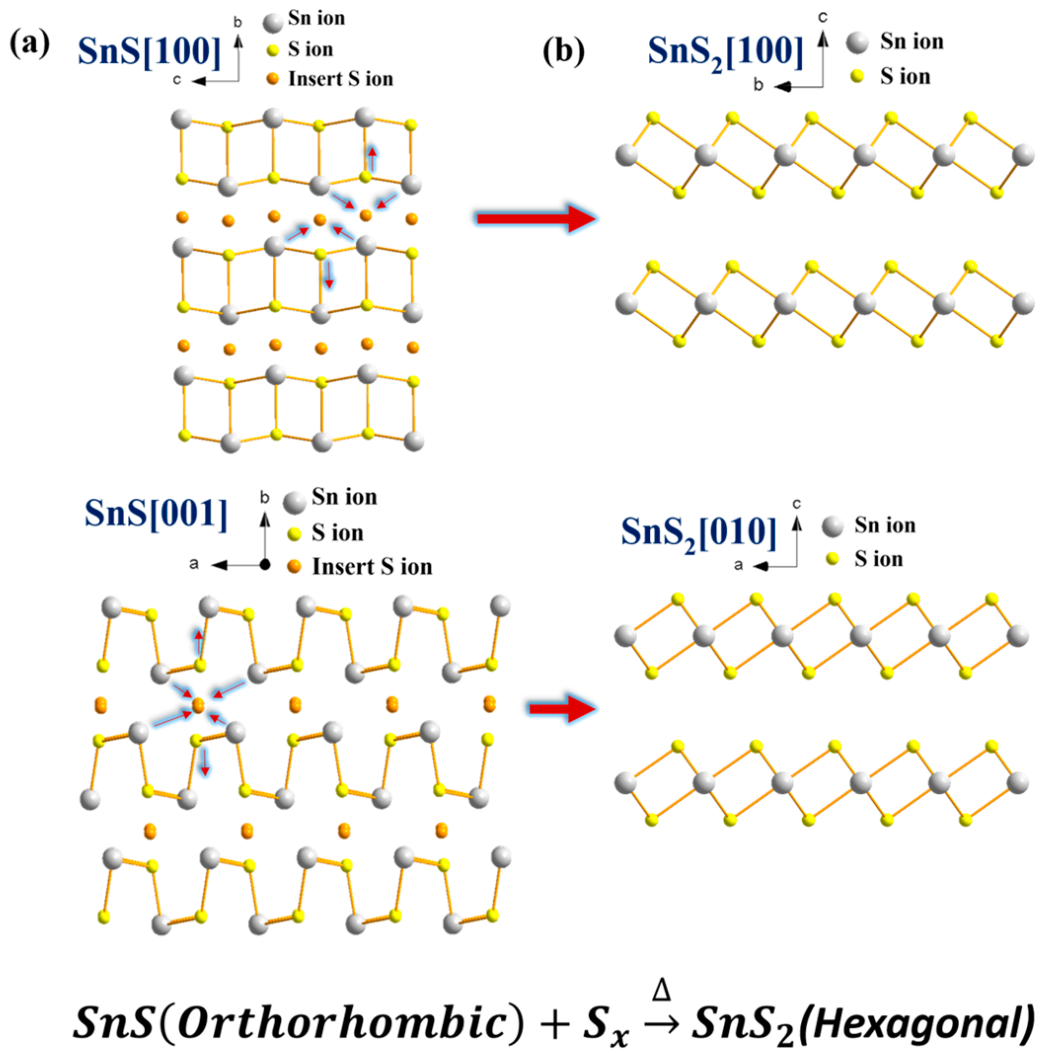
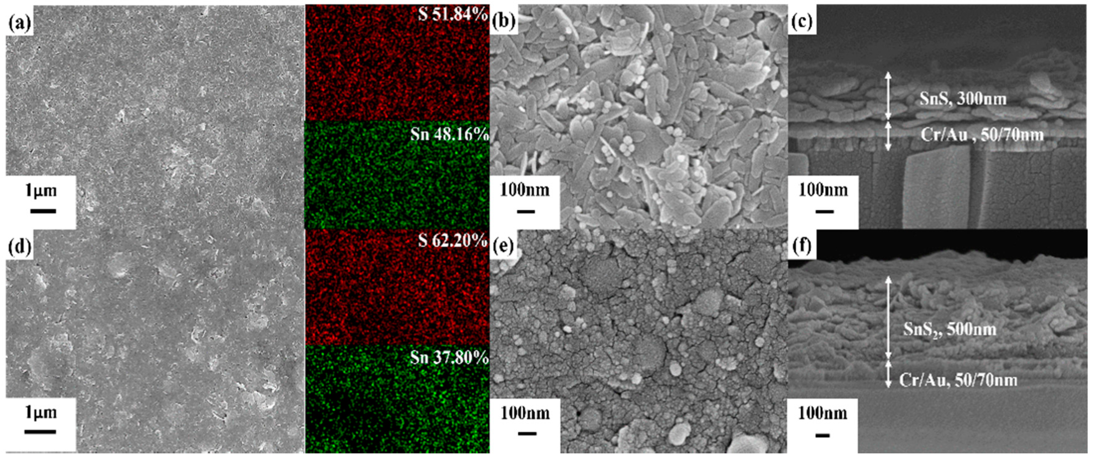
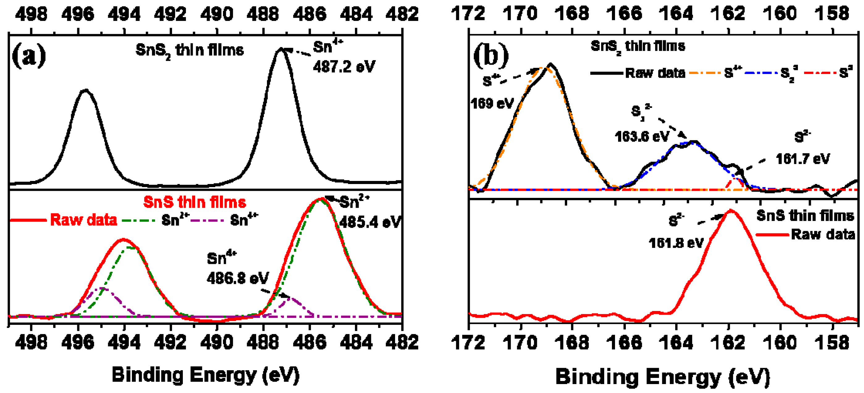
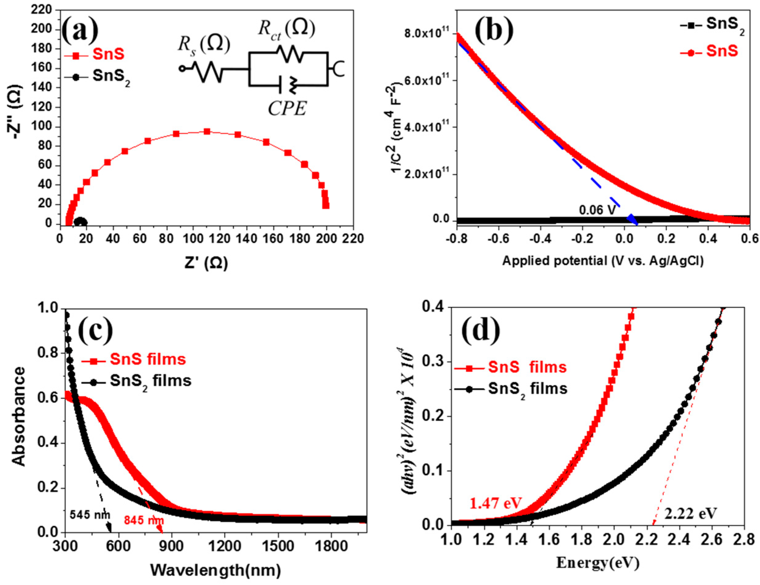
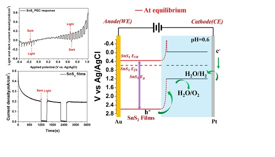
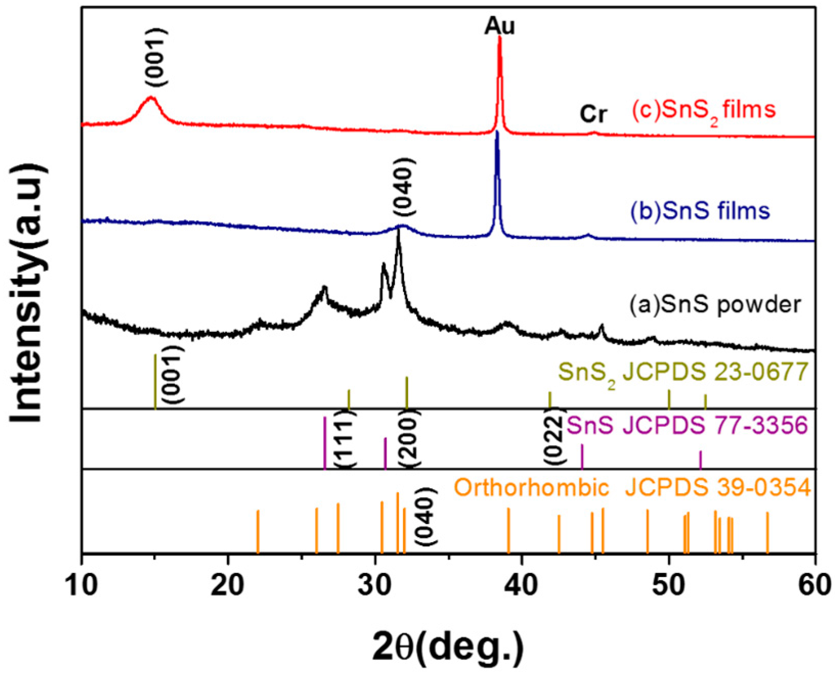
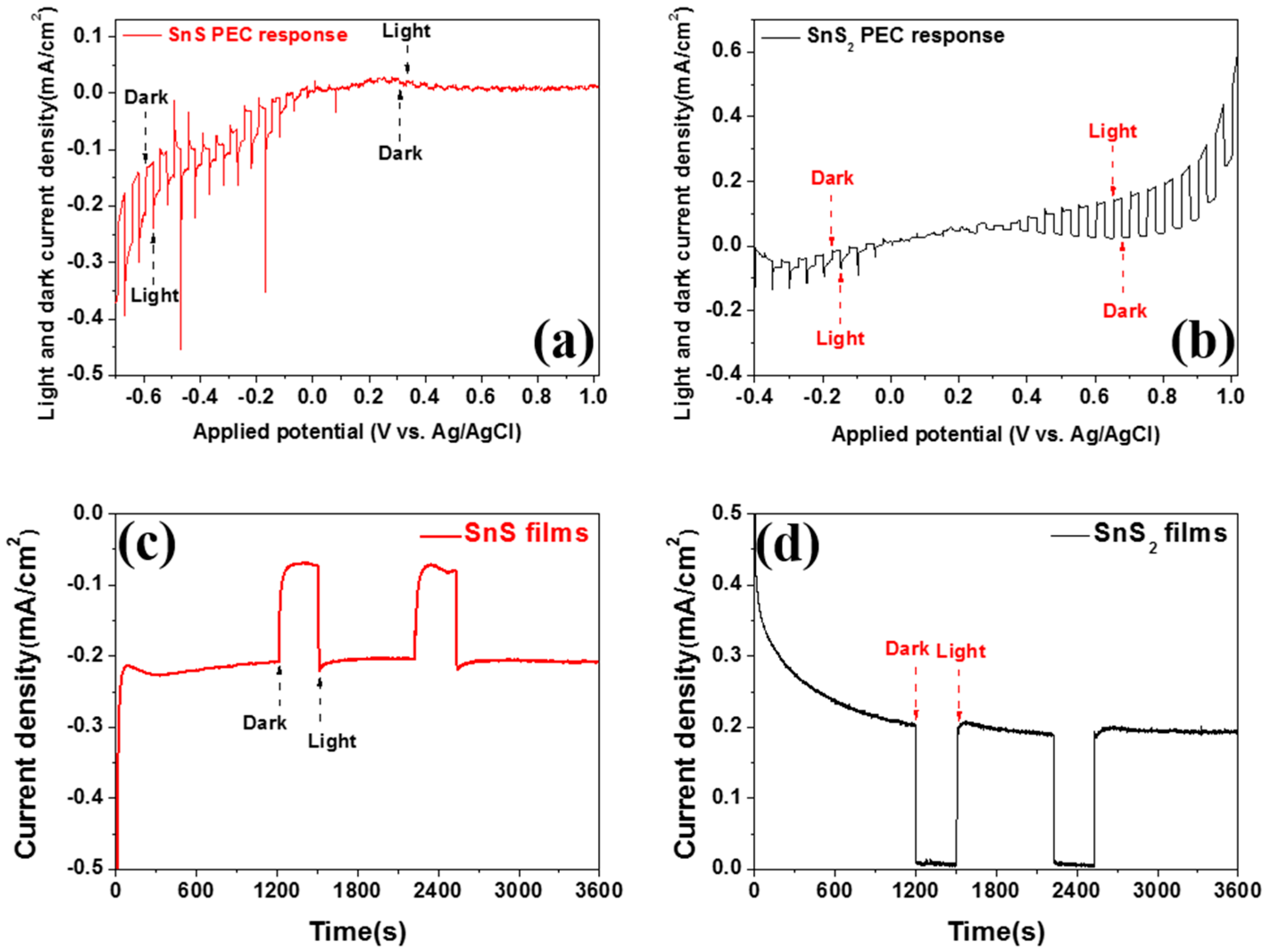
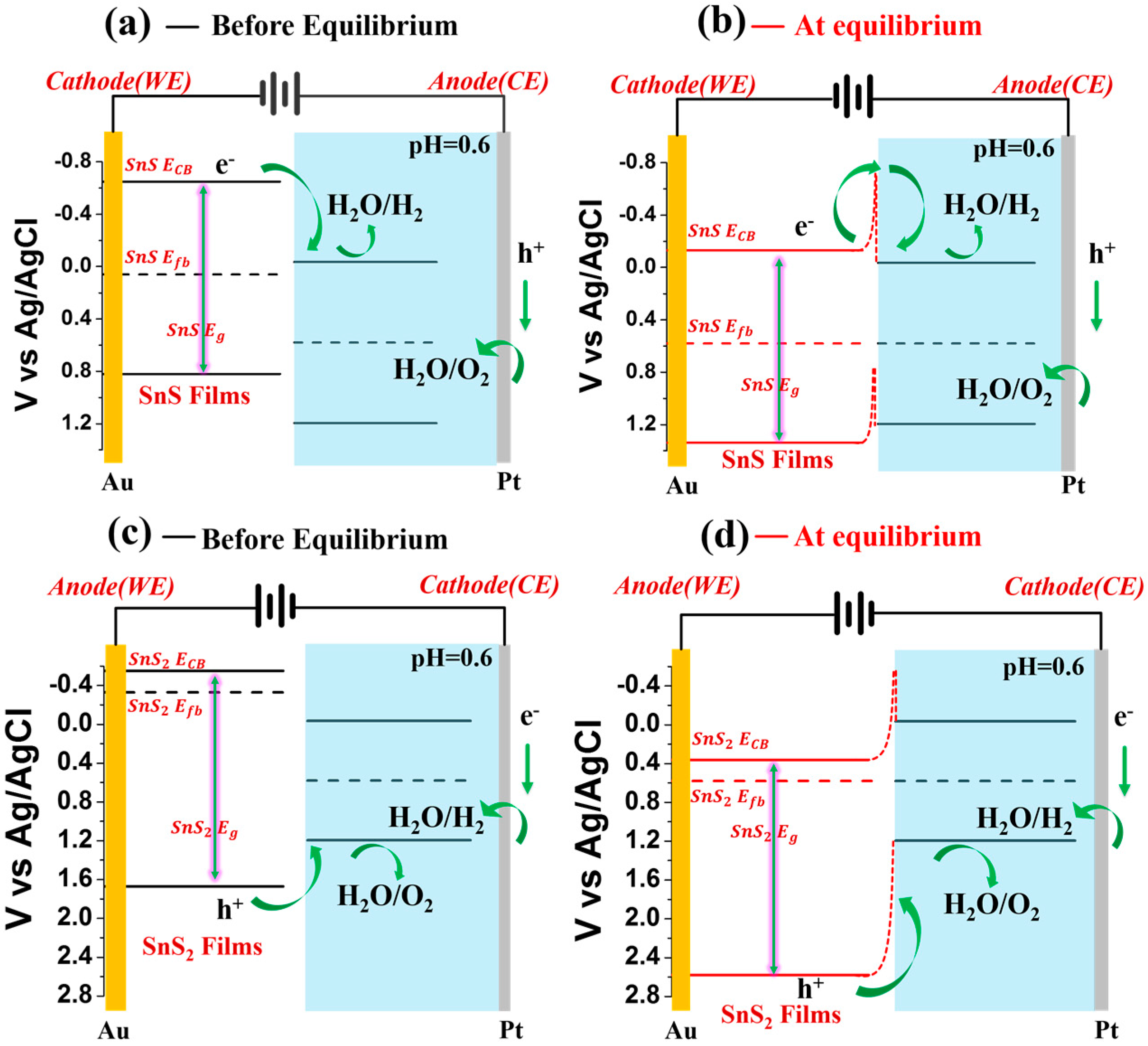
2. Results and Discussion

X-ray diffraction (XRD) analysis of the synthesized SnS nanocrystals confirmed the formation of a mixture of OR-SnS (JCPDFS 39-0354) and cubic-phase SnS (JCPDS 77-3356), as shown in Figure 1a. The detail of mixed-phase SnS is described in our previous reports [33,34]. However, the XRD patterns of SnS thin films deposited by spin coating mixed-phase SnS powder showed a preferred (040) orientation (Figure 1b). After sulfurization, the SnS mixed phase transformed to SnS2 (JCPDS 23-0677) with (001) as the preferred orientation (Figure 1c).
As seen in Figure 2, SnS is inherently a layered material formed by the stacking of (010) planes along the b-axis while SnS2 is also a layered material, but with stacked (001) planes along the c-axis [35,36]. While the S and Sn atoms in a single layer of SnS are bound to each other by strong chemical bonds, individual layers stick together by van der Waals forces [6,37]. We propose a reconstructive growth mechanism where diffusion of sulfur atoms between layers results in the phase transfer of SnS to SnS2. During high temperature sulfurization, the negatively charged S ions are strongly attracted to the positively charged Sn ions, which leads to the formation of distorted SnS layers, as shown in Figure 2a,b. Guo et al. recently reported a similar phase change, where the depletion of sulfur leads to the dissociation of the hexagonal SnS2 phase to the orthorhombic SnS phase during a high temperature process under an argon flow [18].
Figure 3 shows the scanning electron microscopy (SEM) images (top view and cross section) of the SnS and SnS2 thin films. The low magnification images (Figure 3a,d) show compact film formation without any visible cracks exposing the Cr/Au back-contact. The EDX (Energy-dispersive X-ray spectroscopy) elemental mappings of the SnS thin films (insets of Figure 3a,d) reveal uniform distributions of both Sn and S elements (atomic ratio ~1:1, as shown in Supplementary Materials Figure S1), whereas the atomic ratio of SnS2 thin films was approximately 1:2 (Supplementary Materials Figure S2). Moreover, the results from the EDX elemental mapping are in agreement with those obtained from the XRD spectra.
The SnS thin film shows (Figure 3b) collection of sizable clusters comprising of SnS nanocrystals with varying grain size (200~400 nm long and 50~100 nm wide). The solid SnS layer form by the stacking of uniformly dispersed nanocrystals on the substrate throughout the 300 nm thickness of the film as shown in Figure 3c. After intensive sulfurization, the SnS2 thin films (Figure 3e) are more compact than those of the SnS thin films. As observed in Figure 3f, the SnS2 thin film thickness increased to ~500 nm, implying a larger molar volume for the SnS2 phase thin films compared to SnS phase thin films, resulting in the expansion of the films.
The surface electronic states and the chemical composition of the SnS and SnS2 thin films were detected using electron spectroscopy for chemical analysis (ESCA). Figure 4 displays the comparative XPS spectra of Sn and S for the SnS and SnS2 thin films. The SnS2 films (Figure 4a) exhibit two characteristic peaks at 487.2 eV and 495.6 eV corresponding to the 3d5/2 and 3d3/2 of Sn4+, respectively [15,16]. The Sn3d peaks in the SnS thin films were observed at 485.4 eV and 494.0 eV, and can be attributed to the 3d5/2 and 3d3/2 energy levels of Sn2+, respectively [11]. The shift in the Sn3d peaks towards a higher binding energy in SnS2 confirms that all Sn2+ ions were converted to Sn4+ after sulfurization. The S 2p peaks (Figure 4b) in the SnS2 thin films were observed at 161.7 eV (S 2p1/2), 163.6 eV (S 2p3/2), and 169.0 eV, which corresponds to S2−, S22− and sulfone (S4+), respectively [38]. S4+ species behaves more likely as SOx groups, which can be dissolved in the solutions or washed away from the sample [39]. However, the SnS films show a single peak at 161.8 eV (S 2p1/2), indicating the existence of S2− ions in the films [11,16,40].
Moreover, because the SnS thin films are composed of Sn2+ and S2− ions (without other valence states, such as Sn4+ or S22−), they are similar to an intrinsic semiconductor because of the charge neutrality, as shown below:
Sn 2 + + S 2 SnS 0 + ( charge   neutrality )
SnS2 thin films have been sulfurized under vacuum condition. However, in the low vacuum environment, Sn2+ and S2− were oxidized to Sn4+ and S22− or S4+. The intensity of the S22− ions in the S 2p spectrum is much higher compared to that of S2−, which indicates that S22− ions replace S2−, thus leading to the creation of sulfur defects during sulfurization and the consequent generation of shallow donors [41], as shown below:
Sn 4 + + S 2 2 SnS 2 2 +   ( two   free   donor   electrons )
Figure 5 illustrates the electrochemical measurements (such as light on-off linear sweeps, electrochemical impedance spectra, and Mott–Schottky plots) investigated by using a traditional three-electrode measurement system in a 0.25 M H2SO4 (pH = 0.6) electrolyte. The light on-off photoelectrocatalytic response of the SnS and SnS2 thin films varied from −0.7 V to 1 V vs. Ag/AgCl (Figure 5a,b). The SnS thin films display a light-current density of −0.21 mA/cm2 with a sharp peak (Figure 5a) at the applied potential of −0.6 V vs. Ag/AgCl, which implies that a heavy recombination happened during light illumination. SnS thin films show a very weak photocurrent response (less than 0.007 mA/cm2) at 0.8 V vs. Ag/AgCl, which indicates that the SnS thin films work as HER catalysts. In comparison, although the SnS2 thin films do not show high light-current density (less than −0.002 mA/cm2) at −0.4 V vs. Ag/AgCl, they do demonstrate a relatively higher photocurrent density of 0.195 mA/cm2 at 0.8 V vs. Ag/AgCl (Figure 5b). Moreover, the photocurrent response curve does not exhibit a recombination peak that could be attributed to efficient charge transfer during the OER. Stability study of both SnS and SnS2 thin films are shown in Figure 5c,d, where we turned off the solar simulator every 1200–1500 s and 2220–2520 s, respectively, to measure the current during dark and illumination. The SnS thin film displays a light-current of −0.219 and −0.208 mA/cm2 at −0.6 V vs. Ag/AgCl at 600 s and 3600 s, respectively, with negligible fading after 3600 s of light irradiation. However, the SnS2 thin films light-current starts to decrease in the beginning to 1200 s, and light-current of 0.236 and 0.193 mA/cm2 at 0.8 V vs. Ag/AgCl at 600 s and 3600 s are observed. This may be due to the dissolution of S4+ ions leading to the light-current fading. However, after first turn off test, the light-current density becomes stable. The XRD spectra (Supplementary Materials Figure S3) shows that the SnS and SnS2 thin films still maintain the structure even after 3600 s of light irradiation.
Electrochemical impedance spectroscopy (EIS) is a very useful method to analyze PEC performance by investigating the interfacial reactions occurring between the photoelectrode and electrolyte. Figure 6a shows the representative Nyquist plots of the SnS and SnS2 thin film photoelectrodes, which are analyzed by fitting the impedance curve to an equivalent circuit (see inset of Figure 6a), where a constant phase element (CPE) is introduced. The Nyquist plots indicate that the charge-transfer resistance (RCT) of SnS2 (6.16 Ω as shown in Supplementary Materials Figure S4) is much less than SnS (182 Ω), which indicates that the SnS2 thin films exhibit lower interfacial charge-transfer resistance, thereby enhancing the carrier transport/separation efficiency. Put simply, this implies a more efficient transfer of the photogenerated electrons and holes with a significantly reduced recombination rate.
The negative slope in Figure 6b (Mott–Schottky plots) indicates that the SnS thin films are p-type semiconductors, while the positive slope of the SnS2 thin films renders them n-type semiconductors (as shown in Figure S5). Meanwhile, the flat band potential ( E f b ) of the SnS2 thin film is −0.33 V, which was determined by extrapolation of the x-intercepts in Mott–Schottky plots (Supplementary Materials Figure S5); in contrast, a positive potential was observed for the SnS thin film (0.06 V) [42]. In order to better understand the carrier transport of the SnS and SnS2 thin films, we also calculated the carrier density ( N ) as follows:
N = 2 e 0 ε 0 ε r A 2 [ | d ( 1 C 2 ) d V | ] 1
where e 0 is the electron’s charge, ε 0 is the vacuum permittivity, ε r is the dielectric constant of a semiconductor, and A is the actual surface area. The carrier density ( N ) of the SnS2 thin film is about N = 5.08 × 10 18   cm 3 ( ε r = 17.7 ) [16,22], which is 35 times higher than the SnS thin film ( N = 1.43 × 10 17   cm 3 ( ε r = 10.48 ) [43,44]. Generally, photogenerated carriers may undergo recombination due to defects present in the semiconductor before they can be collected or utilized for water splitting. Compared to SnS, the significantly higher carrier density of SnS2 suggests that the photogenerated carriers have a higher probability of participating in the interfacial reactions during water splitting, thus resulting in improved efficiencies. The thickness of the space charge layer ( w ) between the working electrode (SnSx) and the electrolyte at the interface is determined by using the following equation:
w = [ 2 ε 0 ε r ( V V f b ) e 0 N ] 1 2
At an applied potential of 0.8 V, the space charge layer of SnS2 was determined, about 22.6 nm, which is thinner than that of SnS (at −0.6 V, 87.3 nm). This indicates a lower energy barrier between the SnS2 electrocatalyst and the electrolyte, thereby enabling more efficient separation and depletion of charge carriers under an applied potential [45].
Optical measurements of SnS and SnS2 thin films show absorption onsets at about 845 nm and 545 nm (Figure 6c,d). The absorption coefficient ( α ) and energy of the incident photon for semiconductors is related as ( α h v ) n = B ( h v E g ) , where B is a constant and n is a number that depends on the electronic transition of the semiconductor. The dependence of α 2 (for n = 2) on the photon energy ( h v ) for the direct band gap semiconductor is illustrated graphically in Figure 6f. The direct band gaps ( E g ) for the SnS and SnS2 thin films estimated from the intercepts of the plot are 1.47 and 2.22 eV, respectively. Due to quantum confinement effects of 2-D SnS nanosheets, the SnS thin films display the strong blue shift (~0.2 eV) as compared to previously published reports (~1.2eV) [46].
The positions of the conduction bands ( E C B ) for SnS and SnS2 were calculated based on the onset potentials for the reduction reactions of these materials [47]. The conduction band positions for the SnS and SnS2 thin-film electrocatalysts are −0.65 and −0.55 V vs. Ag/AgCl, respectively (Supplementary Materials Figure S6a,b).
The detailed mechanism of PEC water splitting for the SnS and SnS2 photoelectrodes is schematically illustrated in Figure 7. Initially, E f b , E g and E C B were determined by Mott–Schottky plots (as shown in Figure 6b), UV-vis (as shown in Figure 6d) and cyclic voltammograms (as shown in Figure 6a,b), respectively. Details of the band positions before and after equilibrium of the working electrode and the electrolyte are shown in Table 1. The positions of these energy levels before equilibrium were suitable for the transfer of electrons to the electrolyte as well as production of hydrogen or oxygen at the surface of the electrode (Figure 7a,c). However, to understand the actual reaction between electrode and electrolyte, we must consider the positions of all energy levels after thermal equilibrium due to rearrangement of the energy bands, including the flat band position due to the band bending (Figure 7b,d) [48]. The band positions for the SnS and SnS2 thin films during the water splitting reaction have been simulated previously by density functional theory (DFT) [46]. Here, the SnS thin films demonstrated a high carrier density (17 orders) and small energy band gap (~1.47 eV). In addition, the E C B position of SnS after band bending at thermal equilibrium is still above the reduction potential of hydrogen, thus should ideally exhibit good performance for HER. However, the SnS thin films did not show good performance for following reasons: (i) ESCA spectra revealed the intrinsic semiconductor characteristics of SnS thin films (Figure 4); (ii) the E f b position of SnS (0.06 V) was close to the intrinsic Fermi level ( E C B + 1 2 E g = 0.085   V ), which may result in heavy carrier recombination deep inside the SnS thin films; and (iii) the schematic energy level diagram of SnS after thermal equilibrium (Figure 7b) shows an excess barrier at the interface that hinders the water splitting reaction. Comparatively, the SnS2 thin films show good performance as an OER photocatalyst with a higher observed current density, which is attributable to the following reasons: (i) a significantly higher carrier concentration due to defects introduced during sulfurization; (ii) efficient separation of charge carriers and reduced recombination due to the thinner space-charge layer, as demonstrated by the low-charge transfer resistance in the EIS spectra; and (iii) suitable band alignment at the SnS2/aqueous interface for OER.

3. Materials and Methods

3.1. Synthesis of Mixed-Phase SnS Nanocrystals

We followed a standard hot injection procedure for the synthesis of mixed phase SnS nanocrystals consisting of orthorhombic-phase SnS hexagonal nanosheets and cubic-phase SnS nanoparticles by using the reaction conditions as optimized previously [32,33,34,49]. Typically, a predetermined concentration of SnO and oleic acid (1.35 g of SnO (Tin (II) Oxide, SHOWA, 99%, 13.5 mL Oleic Acid, Sigma Aldrich, St. Louis, MO, USA, 66–88%) was taken in a three-neck flask and the mixture was heated to 120 °C under an argon atmosphere for 15 min under continuous stirring to remove moisture. The temperature of the mixture was increased to 280 °C under low vacuum and the turbid mixture was transformed to a transparent clear solution of tin precursor (Sn(OA)X), after which the temperature was decreased to 190 °C. Similarly, the sulfur precursor (S-OLA) was produced by heating the mixture of elemental S powder with 9 mL of oleylamine (0.45 mmol sulfur powder, Sigma Aldrich, St. Louis, MO, USA, 98%, and OLA, ACROS, Boardwalk, NJ, USA, 90%) at 155 °C under continuous stirring in a regular argon flow. The hot sulfur precursor was then rapidly impregnated into the tin precursor by using a glass syringe, and the temperature of the mixture was controlled at 190 °C for 30 min which is then allowed natural cooling to room temperature. The as obtained SnS nanoparticles were collected by centrifugation at 5000 rpm for 15 min. The product was repeatedly washed by ethanol and acetone for the complete removal of the impurity which was then dried in vacuum and re-dispersed in hexane.

3.2. SnS and SnS2 Thin Films Deposition

To prepare the SnS thin films, glass substrates were first coated with Cr/Au (50 nm/70 nm) layers using electron beam physical vapor deposition. The synthesized SnS nanocrystals (20 mg) were dispersed in toluene (2 mL) and spin coated on the glass/Cr/Au substrate followed by vacuum drying for 5 min at 85 °C. The obtained SnS thin films can be converted to SnS2 via a simple annealing step in the presence of S powder. SnS film and S powder (0.1 g) are taken in two different quartz boats and placed 1 cm apart inside a quartz tube. We have used low vacuum conditions (less than 2 torr) for sulfurization. Upon creation of a low vacuum (less than 2 torr), both ends of the quartz tube were sealed and the temperature was raised to 250 °C and held there for 2 h to allow sulfurization to occur. This was followed by cooling the whole system to room temperature.

3.3. SnS and SnS2 Electrochemical Measurements

A three-electrode cell configuration was utilized for electrochemical measurements with Pt as the counter electrode (CE), SnS or SnS2 as the working electrode (WE) and Ag/AgCl (3.0 mol/kg KCl) as the reference electrode (RE) in a 0.25 M H2SO4 electrolyte (pH = 0.6). PEC measurement was carried out by using AM 1.5 simulated sunlight at 100 mW cm−2 (100 W, Model 94011A, Oriel, Irvine, CA, USA) under the applied voltage from −0.7 to 1 V vs. Ag/AgCl. Before doing PEC measurement, nitrogen gas was allowed to flow for 30 min to purge the electrochemical cell and the gas flow was continued until the end of the experiment. A radiometer analytical potentiostat (AutoLab PGSTAT 30) was used to perform photoelectrochemical measurements. Subsequently, linear sweep voltammetry was employed to obtain polarization plots with a fixed scan rate of 5 mV/s. Mott–Schottky plots were used to estimate the data frequency of 1 kHz in the dark and under the applied voltages from −0.8 to 0.6 V vs. Ag/AgCl.

4. Conclusions

In summary, we reported the use of layered SnSx (x = 1, 2) thin films as effective HER and OER photocatalysts for water splitting. A simple, non-toxic hot-injection method was developed for the synthesis of mixed-phase cubic and orthorhombic SnS nanocrystals spin coated on glass/Cr/Au substrates to form compact thin films that serve as the working photoelectrode. SnS thin films can be converted to SnS2 via a facile sulfurization protocol under low vacuum conditions. Moreover, the SnS2 thin films showed good performance for OER due to a higher carrier density, lower interface charge-transfer resistance and an effective band alignment with respect to the electrolyte at equilibrium conditions. Given our encouraging findings, we anticipate future advances in tin sulfide materials as a promising alternative for sustainable water splitting.

Supplementary Materials

Supplementary materials can be found at www.mdpi.com/2073-4344/7/9/252/s1.

Acknowledgments

Authors would like to thank the help from Jih-Jen Wu. This project was financially supported by the Ministry of Science and Technology of the ROC under contract MOST 105-2221-E-218-004- and MOST 104-2221-E-006-032-MY3.

Author Contributions

The manuscript was written through contributions of all authors. All authors have given approval to the final version of the manuscript.

Conflicts of Interest

The authors declare no conflict of interest.

References

  1. Li, X.; Yu, J.G.; Low, J.X.; Fang, Y.P.; Xiao, J.; Chen, X.B. Engineering heterogeneous semiconductors for solar water splitting. J. Mater. Chem. A 2015, 3, 2485–2534. [Google Scholar] [CrossRef]
  2. Chen, X.B.; Shen, S.H.; Guo, L.J.; Mao, S.S. Semiconductor-based photocatalytic hydrogen generation. Chem. Rev. 2010, 110, 6503–6570. [Google Scholar] [CrossRef] [PubMed]
  3. Zhou, M.; Lou, X.W.; Xie, Y. Two-dimensional nanosheets for photoelectrochemical water splitting: Possibilities and opportunities. Nano Today 2013, 8, 598–618. [Google Scholar] [CrossRef]
  4. Fujishima, A.; Honda, K. Electrochemical photolysis of water at a semiconductor electrode. Nature 1972, 238, 37–38. [Google Scholar] [CrossRef] [PubMed]
  5. Sun, Y.F.; Gao, S.; Lei, F.C.; Xie, Y. Atomically-thin two-dimensional sheets for understanding active sites in catalysis. Chem. Soc. Rev. 2015, 44, 623–636. [Google Scholar] [CrossRef] [PubMed]
  6. Butler, S.Z.; Hollen, S.M.; Cao, L.Y.; Cui, Y.; Gupta, J.A.; Gutierrez, H.R.; Heinz, T.F.; Hong, S.S.; Huang, J.X.; Ismach, A.F.; et al. Progress, challenges, and opportunities in two-dimensional materials beyond graphene. ACS Nano 2013, 7, 2898–2926. [Google Scholar] [CrossRef] [PubMed]
  7. Yin, Z.Y.; Chen, B.; Bosman, M.; Cao, X.H.; Chen, J.Z.; Zheng, B.; Zhang, H. Au nanoparticle-modified MoS2 nanosheet-based photoelectrochemical cells for water splitting. Small 2014, 10, 3537–3543. [Google Scholar] [CrossRef] [PubMed]
  8. Sang, Y.H.; Zhao, Z.H.; Zhao, M.W.; Hao, P.; Leng, Y.H.; Liu, H. From UV to near-infrared, WS2 nanosheet: A novel photocatalyst for full solar light spectrum photodegradation. Adv. Mater. 2015, 27, 363–369. [Google Scholar] [CrossRef]
  9. Xie, J.F.; Wang, R.X.; Bao, J.; Zhang, X.D.; Zhang, H.; Li, S.; Xie, Y. Zirconium trisulfide ultrathin nanosheets as efficient catalysts for water oxidation in both alkaline and neutral solutions. Inorg. Chem. Front. 2014, 1, 751–756. [Google Scholar] [CrossRef]
  10. Lei, F.C.; Zhang, L.; Sun, Y.F.; Liang, L.; Liu, K.T.; Xu, J.Q.; Zhang, Q.; Pan, B.C.; Luo, Y.; Xie, Y. Atomic-layer-confined doping for atomic-level insights into visible-light water splitting. Angew. Chem. Int. Ed. 2015, 54, 9266–9270. [Google Scholar] [CrossRef] [PubMed]
  11. Sun, Y.F.; Sun, Z.H.; Gao, S.; Cheng, H.; Liu, Q.H.; Lei, F.C.; Wei, S.Q.; Xie, Y. All-surface-atomic-metal chalcogenide sheets for high-efficiency visible-light photoelectrochemical water splitting. Adv. Energy Mater. 2014, 4, 1300611. [Google Scholar] [CrossRef]
  12. Seal, M.; Singh, N.; McFarland, E.W.; Baltrusaitis, J. Electrochemically deposited sb and in doped tin sulfide (SnS) photoelectrodes. J. Phys. Chem. C 2015, 119, 6471–6480. [Google Scholar] [CrossRef]
  13. Patel, M.; Chavda, A.; Mukhopadhyay, I.; Kim, J.; Ray, A. Nanostructured SnS with inherent anisotropic optical properties for high photoactivity. Nanoscale 2016, 8, 2293–2303. [Google Scholar] [CrossRef]
  14. Kois, J.; Bereznev, S.; Maricheva, J.; Revathi, N. Electrochemical and photoelectrochemical characterization of SnS photoabsorber films. Mater. Sci. Semicon. Proc. 2017, 58, 76–81. [Google Scholar] [CrossRef]
  15. Yu, J.; Xu, C.Y.; Ma, F.X.; Hu, S.P.; Zhang, Y.W.; Zhen, L. Monodisperse SnS2 nanosheets for high-performance photocatalytic hydrogen generation. ACS Appl. Mater. Int. 2014, 6, 22370–22377. [Google Scholar] [CrossRef] [PubMed]
  16. Sun, Y.F.; Cheng, H.; Gao, S.; Sun, Z.H.; Liu, Q.H.; Liu, Q.; Lei, F.C.; Yao, T.; He, J.F.; Wei, S.Q.; et al. Freestanding tin disulfide single-layers realizing efficient visible-light water splitting. Angew. Chem. Int. Ed. 2012, 51, 8727–8731. [Google Scholar] [CrossRef] [PubMed]
  17. An, X.Q.; Yu, J.C.; Tang, J.W. Biomolecule-assisted fabrication of copper doped SnS2 nanosheet-reduced graphene oxide junctions with enhanced visible-light photocatalytic activity. J. Mater. Chem. A 2014, 2, 1000–1005. [Google Scholar] [CrossRef]
  18. Zhou, T.F.; Pang, W.K.; Zhang, C.F.; Yang, J.P.; Chen, Z.X.; Liu, H.K.; Guo, Z.P. Enhanced sodium-ion battery performance by structural phase transition from two-dimensional hexagonal-SnS2 to orthorhombic-SnS. ACS Nano 2014, 8, 8323–8333. [Google Scholar] [CrossRef] [PubMed]
  19. Tripathi, A.M.; Mitra, S. Tin sulfide (SnS) nanorods: Structural, optical and lithium storage property study. RSC Adv. 2014, 4, 10358–10366. [Google Scholar] [CrossRef]
  20. Shinde, S.S.; Sami, A.; Kim, D.H.; Lee, J.H. Nanostructured SnS-n-doped graphene as an advanced electrocatalyst for the hydrogen evolution reaction. Chem. Commun. 2015, 51, 15716–15719. [Google Scholar] [CrossRef] [PubMed]
  21. Koktysh, D.S.; McBride, J.R.; Geil, R.D.; Schmidt, B.W.; Rogers, B.R.; Rosenthal, S.J. Facile route to SnS nanocrystals and their characterization. Mater. Sci. Eng. B Adv. 2010, 170, 117–122. [Google Scholar] [CrossRef]
  22. Takeda, N.; Parkinson, B.A. Adsorption morphology, light absorption, and sensitization yields for squaraine dyes on SnS2 surfaces. J. Am. Chem. Soc. 2003, 125, 5559–5571. [Google Scholar] [CrossRef] [PubMed]
  23. Devika, M.; Reddy, K.T.R.; Reddy, N.K.; Ramesh, K.; Ganesan, R.; Gopal, E.S.R.; Gunasekhar, K.R. Microstructure dependent physical properties of evaporated tin sulfide films. J. Appl. Phys. 2006, 100, 023518. [Google Scholar] [CrossRef]
  24. Mitzi, D.B.; Kosbar, L.L.; Murray, C.E.; Copel, M.; Afzali, A. High-mobility ultrathin semiconducting films prepared by spin coating. Nature 2004, 428, 299–303. [Google Scholar] [CrossRef] [PubMed]
  25. Reddy, K.T.R.; Reddy, N.K.; Miles, R.W. Photovoltaic properties of SnS based solar cells. Sol. Energy Mater. Sol. C 2006, 90, 3041–3046. [Google Scholar] [CrossRef]
  26. Thangaraju, B.; Kaliannan, P. Spray pyrolytic deposition and characterization of SnS and SnS2 thin films. J. Phys. D Appl. Phys. 2000, 33, 1054–1059. [Google Scholar] [CrossRef]
  27. Avellaneda, D.; Nair, M.T.S.; Nair, P.K. Polymorphic tin sulfide thin films of zinc blende and orthorhombic structures by chemical deposition. J. Electrochem. Soc. 2008, 155, D517–D525. [Google Scholar] [CrossRef]
  28. Avellaneda, D.; Nair, M.T.S.; Nair, P.K. Photovoltaic structures using chemically deposited tin sulfide thin films. Thin Solid Films 2009, 517, 2500–2502. [Google Scholar] [CrossRef]
  29. Patel, M.; Ray, A. Evaluation of back contact in spray deposited SnS thin film solar cells by impedance analysis. ACS Appl. Mater. Int. 2014, 6, 10099–10106. [Google Scholar] [CrossRef]
  30. Kafashan, H.; Azizieh, M.; Vatan, H.N. Ultrasound-assisted electrodeposition of SnS: Effect of ultrasound waves on the physical properties of nanostructured SnS thin films. J. Alloy Compd. 2016, 686, 962–968. [Google Scholar] [CrossRef]
  31. Chaki, S.H.; Chaudhary, M.D.; Deshpande, M.P. Effect of indium and antimony doping on SnS photoelectrochemical solar cells. Chin. Phys. Lett. 2014, 31, 106102. [Google Scholar] [CrossRef]
  32. Liang, B.Y.J.; Shen, Y.M.; Wang, S.C.; Huang, J.L. The influence of reaction temperatures and volume of oleic acid to synthesis SnS nanocrystals by using thermal decomposition method. Thin Solid Films 2013, 549, 159–164. [Google Scholar] [CrossRef]
  33. Huang, P.C.; Huang, J.L.; Wang, S.C.; Shaikh, M.O.; Lin, C.Y. Photoelectrochemical properties of orthorhombic and metastable phase sns nanocrystals synthesized by a facile colloidal method. Thin Solid Films 2015, 596, 135–139. [Google Scholar] [CrossRef]
  34. Huang, P.C.; Shaikh, M.O.; Wang, S.C. Structural and optoelectronic properties of alloyed snxmn1-xs thin films. Adv. Powder Technol. 2016, 27, 964–970. [Google Scholar] [CrossRef]
  35. Reddy, N.K. Growth-temperature dependent physical properties of SnS nanocrystalline thin films. ECS J. Solid State Sci. Technol. 2013, 2, P259–P263. [Google Scholar] [CrossRef]
  36. Han, J.H.; Lee, S.; Cheon, J. Synthesis and structural transformations of colloidal 2d layered metal chalcogenide nanocrystals. Chem. Soc. Rev. 2013, 42, 2581–2591. [Google Scholar] [CrossRef] [PubMed]
  37. Herron, S.M.; Tanskanen, J.T.; Roelofs, K.E.; Bent, S.F. Highly textured tin(ii) sulfide thin films formed from sheetlike nanocrystal inks. Chem. Mater. 2014, 26, 7106–7113. [Google Scholar] [CrossRef]
  38. Freeman, T.L.; Evans, S.D.; Ulman, A. Xps studies of self-assembled multilayer films. Langmuir 1995, 11, 4411–4417. [Google Scholar] [CrossRef]
  39. Koroteev, V.O.; Bulusheva, L.G.; Asanov, I.P.; Shlyakhova, E.V.; Vyalikh, D.V.; Okotrub, A.V. Charge transfer in the MoS2/carbon nanotube composite. J. Phys. Chem. C 2011, 115, 21199–21204. [Google Scholar] [CrossRef]
  40. Chang, Y.H.; Wu, F.Y.; Chen, T.Y.; Hsu, C.L.; Chen, C.H.; Wiryo, F.; Wei, K.H.; Chiang, C.Y.; Li, L.J. Three- dimensional molybdenum sulfi de sponges for electrocatalytic water splitting. Small 2014, 10, 895–900. [Google Scholar] [CrossRef]
  41. Lin, Y.J.; Lee, C.S.; Lee, C.T. Investigation of accumulated carrier mechanism on sulfurated gan layers. J. Appl. Phys. 2003, 93, 5321–5324. [Google Scholar] [CrossRef]
  42. Wang, G.M.; Ling, Y.C.; Wang, H.Y.; Yang, X.Y.; Wang, C.C.; Zhang, J.Z.; Li, Y. Hydrogen-treated WO3 nanoflakes show enhanced photostability. Energy Environ. Sci. 2012, 5, 6180–6187. [Google Scholar] [CrossRef]
  43. Gedi, S.; Reddy, V.R.M.; Park, C.; Chan-Wook, J.; Reddy, K.T.R. Comprehensive optical studies on SnS layers synthesized by chemical bath deposition. Opt. Mater. 2015, 42, 468–475. [Google Scholar] [CrossRef]
  44. Jakhar, A.; Jamdagni, A.; Bakshi, A.; Verma, T.; Shukla, V.; Jain, P.; Sinha, N.; Arun, P. Refractive index of SnS thin nano-crystalline films. Solid State Commun. 2013, 168, 31–35. [Google Scholar] [CrossRef]
  45. Yang, X.Y.; Wolcott, A.; Wang, G.M.; Sobo, A.; Fitzmorris, R.C.; Qian, F.; Zhang, J.Z.; Li, Y. Nitrogen-doped zno nanowire arrays for photoelectrochemical water splitting. Nano Lett. 2009, 9, 2331–2336. [Google Scholar] [CrossRef] [PubMed]
  46. Shiga, Y.; Umezawa, N.; Srinivasan, N.; Koyasu, S.; Sakai, E.; Miyauchi, M. A metal sulfide photocatalyst composed of ubiquitous elements for solar hydrogen production. Chem. Commun. 2016, 52, 7470–7473. [Google Scholar] [CrossRef] [PubMed]
  47. Shown, I.; Hsu, H.C.; Chang, Y.C.; Lin, C.H.; Roy, P.K.; Ganguly, A.; Wang, C.H.; Chang, J.K.; Wu, C.I.; Chen, L.C.; et al. Highly efficient visible light photocatalytic reduction of CO2 to hydrocarbon fuels by cu-nanoparticle decorated graphene oxide. Nano Lett. 2014, 14, 6097–6103. [Google Scholar] [CrossRef] [PubMed]
  48. Kibria, M.G.; Zhao, S.; Chowdhury, F.A.; Wang, Q.; Nguyen, H.P.T.; Trudeau, M.L.; Guo, H.; Mi, Z. Tuning the surface fermi level on p-type gallium nitride nanowires for efficient overall water splitting. Nat. Commun. 2014, 5, 3825–3831. [Google Scholar] [CrossRef] [PubMed]
  49. Huang, P.C.; Wang, H.I.; Brahma, S.; Wang, S.C.; Huang, J.L. Synthesis and characteristics of layered SnS2 nanostructures via hot injection method. J. Cryst Growth 2017, 468, 162–168. [Google Scholar] [CrossRef]
Figure 1. XRD pattern for: (a) SnS nanocrystals; (b) SnS thin film; and (c) SnS2 thin film.
Catalysts 07 00252 g001
Figure 2. Schematic of proposed growth mechanism for the phase transition process of SnS to SnS2 via sulfurization. Different sectional views of atomic arrangements of: (a) orthorhombic SnS; and (b) hexagonal SnS2 (atom color: gray, tin; yellow, sulfur; orange, insert sulfur).
Catalysts 07 00252 g002
Figure 3. Top and cross sectional SEM image of: (ac) SnS thin films; and (df) SnS2 thin films (after sulfurization).
Catalysts 07 00252 g003
Figure 4. (a) ESCA (electron spectroscopy for chemical analysis) spectra displays Sn 3d5/2 and Sn 3d5/2 peaks at 487.2 eV and 485.4 eV corresponding to Sn4+ and Sn2+ of SnS2 and SnS thin films, respectively; and (b) S 2p3/2 and S 2p1/2 peaks at 161.8 and 163.6 eV that matches the binding energy of S2− and S22− of SnS2 and SnS thin films, respectively.
Catalysts 07 00252 g004
Figure 5. Linear sweep voltammetry plots for light on-off were recorded in 100 mW/cm2 illumination and dark, respectively, at a scan rate of 5 mV/s for: (a) SnS thin film; and (b) SnS2 thin film. Stability study of: (c) SnS thin film at −0.6 V vs. Ag/AgCl; and (d) SnS2 thin film at 0.8 V vs. Ag/AgCl for 3600 s.
Catalysts 07 00252 g005
Figure 6. (a) Electrochemical impedance spectra (EIS) for SnS thin films at an applied ac potential of −0.6 V and SnS2 thin films is 0.8 V where Z′ and Z″ are the real and imaginary parts of impedance, respectively, while the solid lines were fitted by NOVA software using the equivalent circuits; (b) Mott–Schottky plots of SnS and SnS2 thin films at a scan rate of 5 mV/s (CE: Pt); (c) UV-Vis absorption spectra as a function of incident photon wavelength; and (d) direct bandgap of SnS and SnS2 thin films.
Catalysts 07 00252 g006
Figure 7. Schematic energy levels of SnS: (a) before; and (b) at equilibrium; and for SnS2: (c) before; and (d) at equilibrium.
Catalysts 07 00252 g007
Table 1. The details of the band positions before and at equilibrium.
Before Equilibrium (V vs. Ag/AgCl)At Equilibrium (V vs. Ag/AgCl)
Conduction Band ( E C B )Band Gap ( E g )Flat Band ( E f b )Conduction Band ( E C B )Band Gap ( E g )Flat Band ( E f b )
SnS−0.65 V1.47 eV0.06 V−0.131.47 eV0.58 V
SnS2−0.55 V2.22 eV−0.33 V0.36 V2.22 eV0.58 V
Reduction Potential ( E h )Band Gap ( E g )Fermi Level ( E F )Reduction Potential ( E h )Band Gap ( E g )Fermi Level ( E F )
H2SO4 (pH = 0.6)−0.035 V1.23 eV0.58 V−0.035 V1.23 eV0.58V

