Abstract
In recent years, perovskite solar cells have achieved high efficiency in small areas, but the industrialization of perovskite solar cells is still hampered by the efficiency loss of cells during area scaling. Series modules are currently the most widely used and effective modular process for perovskite solar cells, a process that requires the patterning of the layer stack in individual cells. This interconnection scheme consists of three lines, P1–P3, which are ablated using a pulsed laser beam. In this work, we developed an efficient perovskite module with a high geometric fill factor (GFF) based on a two-step spin-coating method by optimizing the laser ablation step. We constructed the entire device structure by means of a picosecond green pulsed laser, meanwhile, the dead area is greatly reduced by optimizing the parameters and process, and finally achieving an ultra-high GFF of over 99%. In addition, we investigated the effect of poor P2 and P3 ablation on the perovskite solar modules and compared the performance of the module before and after ablation optimization. We finally obtained a maximum photoelectric conversion efficiency of 22.79% with an aperture area of 12.6 cm2. Concurrently, we conducted electrocatalytic hydrogen production experiments on the prepared perovskite solar modules, and the experimental results have also shown excellent performance and good prospects.
1. Introduction
The rapid development in the efficiency of hybrid perovskite solar cells (PSCs) over the past decade has made this emerging photovoltaic (PV) technology a promising PV technology for the PV market [1,2,3]. In addition, it has a broad prospect in solar photovoltaic power generation, photoelectric catalysis, and electrolytic water hydrogen production. As a next step, it is to be manufactured on a module scale to meet commercialization requirements for further practical applications [4,5]. The area of perovskite solar modules (PSMs) and their efficiency and stability improvements have recently become an intense area of research for major groups and companies. In the past decade, the photovoltaic conversion efficiency (PCE) of small cells with an effective area of 0.1 cm2 has soared to 25.8%, which is comparable to the efficiency of other popular types of solar cells [6,7,8]. With the outstanding efficiency of small-area devices, research efforts are gradually shifting to other important issues that need to be addressed for commercialization, such as scalability and stability.
In general, perovskite solar modules (PSMs) have the same functional layers as perovskite solar cells (PSCs), including transparent conducting oxide (TCO) substrates, charge (electron and hole) transport layers, perovskite layers, and metal electrodes [9]. However, it is impractical to construct PSMs in the same form as PSCs due to the non-negligible increase in square resistance of TCO over long distances. To minimize current losses, PSMs can be fabricated by connecting isolated neighboring sub-cells in series or parallel to form modules [10].
In recent years, researchers have made many advances in addressing the scientific and technical challenges of developing efficient and stable PSMs [11,12,13]. Typically, the most important challenge is to reduce efficiency losses as the device area increases from the cell level to the module scale [14]. The efficiency difference between small-area devices and large-area modules is usually attributed to the following: (1) poor module current collection due to increased series resistance, resulting in significant current losses [15]; (2) reduced parallel resistance of module devices due to uneven coating of the perovskite absorbing layer and other interface layers [7]; (3) poor contact in the interconnection region of individual sub-cells in module fabrication and laser scribing process unavoidable dead areas [16]. Currently, the main module interconnection manufacturing methods are series and parallel methods. Series-connected micromodules can produce a high total voltage proportional to the number of sub-cells, while their photocurrent is limited by the photocurrent of individual sub-cells [17]. In contrast, parallel-connected micromodules can produce a high total current equivalent to the sum of sub-cells and a low photovoltage equivalent to that of a single sub-cell [18]. Since the current loss of the transparent conducting electrodes is more severe, the low current of the series method can reduce the loss, while the parallel method generates more loss, and the more efficient series method is now mainly used. Thus far, most of the reported PSMs for perovskite modules have been based on series-connected designs [19], in which the module is divided into several strips of sub-cells, and the neighboring sub-cells are connected by an interconnection region consisting of P1, P2, and P3 lines formed by a laser process [20]. These three lines must be parallel to each other to avoid unnecessary mutual interference. The proper safety distance between the three lines and the proper width of each line is also important to achieve the desired functionality and to avoid undesired leakage or losses [21,22]. In PSMs based on a series configuration, P1 lines are typically drawn on the TCO substrate to isolate adjacent sub-cells and to plan all areas of the entire cell before depositing the charge transport and perovskite layers [23]. After depositing the electron transport layer, the perovskite layer, and the hole transport layer, a laser is used to completely remove the entire area of the charge (electron or hole) transport layer/perovskite/charge (hole or electron) transport layer, while ensuring that the TCO substrate is not damaged. Since the P2 line is the channel that creates the series electrical connection from the top metal electrode of one sub-cell to the bottom TCO electrode of an adjacent sub-cell after depositing the top electrode, it is important to obtain a clean P2 line with the proper width to ensure good ohmic contact between the top electrode and the TCO substrate [21]. In some cases, when ultra-thin charge transfer layers with high conductivity are used, the bottom charge transfer layer is allowed to remain on the TCO substrate in the P2 channel due to the limited resistance loss [24,25,26]. After the vaporization of the metal electrodes is completed, P3 lines are ablated on the top metal electrodes to isolate the adjacent sub-cells. Finally, the laser P4 process is used to clear the edges to obtain series-connected perovskite solar modules [27,28]. It is important to note that the P1–P2–P3 interconnection area is called the “dead area”, i.e., the inactive area that does not participate in module power generation. To increase the total power generation for a given module area, the P1–P2–P3 interconnection area should be minimized to increase the ratio of the active power generation area to the total aperture area. This ratio is defined as the geometric fill factor (GFF) and it can be calculated as a percentage of the active area/total aperture area. The ultimate goal of the laser process is to increase the GFF without compromising efficiency; thus, obtaining a perovskite module with the smallest dead area [29,30].
Nowadays, with the increasing maturity of PSCs, photovoltaic power generation is only one part of the process. We need to explore and practice more application directions to bring new opportunities for the development of PSCs. Hydrogen has been hailed as the “ultimate energy” to control the rising temperature of the earth and solve the energy crisis in the 21st century [31]. Hydrogen can effectively compensate for the poor storage capacity of electrical energy and support the development of a high proportion of renewable energy [32].
The hydrogen energy industry is developing rapidly and has been commercialized in the field of hydrogen fuel cell vehicles [33,34]. Hydrogen production by electrolysis of water from renewable energy sources has a purity of 99.999% and can be directly applied to fuel cell vehicles after a simple drying process, saving the cost of hydrogen production from fossil energy sources and the high energy-consuming purification of hydrogen by-products. Hydrogen production by water electrolysis, especially through renewable energy generation, can not only achieve a green and clean life cycle but also expand the scope of renewable energy utilization. To meet the new demand for hydrogen energy in mass transportation, there is an urgent need to develop clean power water electrolysis hydrogen production technology.
In recent years, PSMs have seen relatively rapid development with some exciting results. In 2015 Qiu et al. [35] achieved an efficiency of 10.4% on an area of 10.1 cm2 using a scraping method, while they also tried it on an area of 100 cm2 but the efficiency decayed to 4.3%; this was the first time that the difficulty of area scaling for PSCs was recognized. After this, researchers mainly focused on small-area PSMs (< 100 cm2). In 2017, Agresti et al. [36] achieved an efficiency of 12.6% on an area of 50.6 cm2 using spin-coating, and the following year Yang et al. [24] prepared a 10.36 cm2 module by scraping, achieving an efficiency of 15.6%. In the latter years, the efficiency of PSMs achieved faster progress with the development of PSCs, and in 2020, Du et al. [37] achieved 19.6% efficiency on an area of 7.92 cm2 by slit coating, and in 2021, UtmoLight Ltd. from China achieved a stable series minimum module efficiency of 20.1% with an aperture area of 63.98 cm2 [38]. This is the first time that the efficiency of PSMs exceeded 20%. In the same year, Bu et al. [17] also achieved an efficiency of 20.42% on an area of 17.1 cm2 by slit coating, and as of March 2022, Song-Yuan Dai’ et al. [1] achieved a record efficiency of 22.7% with an aperture area of 24 cm2 and has not been surpassed thus far. These results are based on series devices, although significant progress has been made on parallel modules, which have been reported to a lesser extent. Recently, Chen et al. [18] achieved a certified quasi-stable efficiency of 16.63% and an effective area of 20.77 cm2 for the parallel module. The most widely used is the series connected PSMs, a structure that reduces the electrical losses of perovskite during area scaling and maximizes the module’s efficiency, which is currently superior compared to parallel modules. However, almost all current PSMs have a GFF below 95%, which means at least 5% of the power generating area is lost, which is a great loss. For small area modules, only the effective area of the cell is counted for efficiency certification, i.e., the dead area is removed, so researchers generally make the dead width wider to ensure proper laser scribing function. However, for industrialization, what matters is the efficiency of the whole module aperture area, not just the efficiency of the effective area after removing the dead area. Furthermore, as the area of the PSMs expands, the dead area will further expand, and this part of the efficiency loss is what we must try to reduce. In sum, it is necessary to optimize the laser process of the chalcogenide module to achieve a smaller dead area and higher GFF. Ballif et al. [39] first reported laser-scribed PSMs in 2015 with a GFF of 84% by using a nanosecond (ns) pulse laser. In 2021, Huang et al. [17] gained an active area PCE of 20.4% for a PSM by utilizing a femtosecond (fs) pulse laser, starting from a PCE of PSC of 23.35%. Recently, an active area PCE of 21.4% was achieved by Naseeruddin et al. for their PSMs, while the GFF was as high as 90.2% [40]. Seok et al. [41] achieved an aperture area efficiency of 20.4% and a GFF of 94.36% by using a picosecond laser. In 2022, Negand et al. [42] achieved a very respectable GFF of 94.7% with a PCE of 19.1% (aperture area of 12.25 cm2) using a custom laser scribing device. Park et al. [43] achieved a high GFF of 95.5% and PCE of 21.07% (aperture area of 12.96 cm2) by using a nanosecond laser and fine lifting off the capping layers on indium tin oxide and identifying the residue within the scribed area. The current work is not perfect in optimizing the dead width of PSMs, and there is still much room for improvement.
In this paper, the laser process for perovskite modules was optimized using picosecond lasers. The main purpose of these optimizations is to reduce the dead area of the module while ensuring the functionality of P1, P2, and P3, and to increase the module efficiency by increasing the GFF. The final optimization of up to 99% GFF allows us to have only very low losses in the area scaling process and finally achieve a 22.69% photoelectric conversion efficiency. We also experimented with the electrolysis of water for hydrogen production using the prepared modules. The experimental results were more exciting, and hydrogen was successfully prepared by photocatalysis of the PSMs, using simulated sunlight as an energy source.
2. Results and Discussion
To develop a simple, stable, and reproducible process that can be directly extended to the perovskite module, the interconnection of module subunits was achieved by using a green laser (λ = 532 nm) with a pulse width of 20 ns and an infrared laser (λ = 1064 nm) in an ablation sequence of P1, P2, and P3, as shown in Figure 1. The expected module layout consists of six cells connected in series, each with an effective area of about 2.1 cm2, a total aperture area of 12.6 cm2, and a module structure of ITO/SnO2/Perovskite/spiro-OMeTAD/Au. All the laser processes are schematically reproduced in Figure 1, where the laser scribing areas of P1, P2, and P3 are shown in Figure 1b.
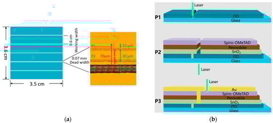
Figure 1.
(a) Schematic diagram of the distribution of active and dead areas of PSMs and microscopic images of laser P1, P2, and P3 ablation areas. (b) Perovskite module structure and laser P1, P2, and P3 scribing schematic.
The laser devices P1, P2, and P3 used in this experiment are 532 nm green laser devices and P4 laser devices are 1064 nm infrared laser devices, which are manufactured by Shenzhen Kyowa Intelligent Technology Co. We conducted a comparison between 1064 nm infrared light and 532 nm green light scribing in laser P1 to investigate the effects of the two lasers on the removal efficiency and scribing width of ITO; we mainly investigated the effects of P2 laser energy, pulse repetition frequency (PRF), and laser spot size on the scribing effect, focusing on the effects of different P2 scribing quality on the performance of the module; last, laser P3 focused on the effect of different laser incidence directions on the scribing effect and its effect on the performance of the module. The purpose of all these optimizations was to reduce the width of the dead area while ensuring the normal laser scribing function. After the optimization, the dead area width of the module was reduced from 150 μm to 70 μm, and the final GFF of the module was >99%.
2.1. P1 Laser Process
The large area TCO glass substrate needs to first be patterned by a laser process (called P1) before it can be used to achieve parallel scribing and ultimately determine the total area of each solar cell used to make up the module, i.e., the cell area, the sink bar area, and the subsequent clear edge area that needs to be removed using P4.
As shown in Figure 2a, the expected module layout consists of six series-connected cell sub-cells, each with an effective area of about 2.1 cm2 and a module structure of ITO/SnO2/Perovskite/spiro-OMeTAD/Au. Due to the high absorption of both green and IR light by ITO, P1 scribing was easily achieved on the ITO/glass substrate, as the only requirement for P1 is that it must be completely electrically isolated and the cells on both sides of P1 must be completely insulated, i.e., the ITO must be completely removed from the P1 ablated area. Since P1 only needs to remove the ITO layer, and ITO absorbs light at all wavelengths relatively well, we tried the available green laser at 532 nm and the infrared laser at 1056 nm. As shown in Figure 2b, the 532 nm green light and 1064 nm infrared light were used to laser ablate the ITO glass, and both were found to be effective in isolating the bottom electrode of the battery, and both were tested with a multimeter and found to be completely insulated, as shown in Table 1.
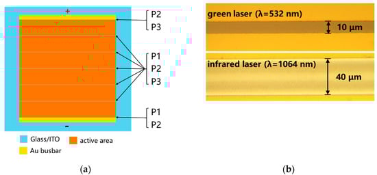
Figure 2.
(a) Laser P1 process scribing pattern and the distribution of each functional area. (b) Optical microscope image of 532 nm green laser with 1064 nm IR laser P1 ablation.

Table 1.
Width and resistance of the ablated area after P1 ablation with different wavelength lasers.
As can be seen from Figure 2b and Table 1, the P1 of the two-laser scribing differs in width. Since the green light has a smaller spot and more concentrated energy, the width of the cut P1 can be controlled at about 10 μm, while the width of the P1 cut by infrared light will basically exceed 40 μm. Although both laser scribing achieves the function of the planning area and dividing of ion cells, it is difficult to reduce the width of P1 after infrared laser scribing, which will lead to a larger increase in the dead area; hence, the subsequent selection of the narrower width of the green laser to cut P1.
2.2. P2 Laser Process
After the deposition of the SnO2 layer, the perovskite layer, and the spiro-OMeTAD layer, a second laser scribing (called the P2 process) is required to clean out the area where the bottom electrode and the top electrode of the subsequent vapor deposition interconnect vertically. Although laser patterning is considered by the research community as the most desirable technique for fabricating perovskite modules in an industrial environment and is relatively easy to implement, the P2 laser scribing process is not a simple step. In fact, it should achieve complete removal of the ETL (SnO2)/perovskite/HTL (spiro-OMeTAD) triple-layer structure without damaging the underlying transparent conductive electrode (ITO), ensuring minimum contact resistance between the ITO and the top Au electrode vertical interconnects. The focus in developing efficient interconnects is the optimization of the P2 process. This requires careful tuning of the laser parameters to optimize the balance between incomplete interlayer removal at low laser fluence and ITO damage at high laser fluence.
As shown in Figure 3a, we first chose to adjust the laser power to cut P2, since laser power is the most important factor in determining the scribing results. At higher laser power, the ITO may be damaged, leading to an increase in the series resistance Rs, while lower laser energy will lead to incomplete removal of the film layer above the ITO and affect the contact between the metal electrode and it; thus, the laser power must find a moderate range. As shown in Figure 3a, the P2 laser ablated area has the best morphology only when the power is between 0.45–0.5 W. The balance between incomplete removal and ITO damage is achieved. As shown in Table 2, at higher energy, P2 can cause irreversible damage to the cell and reduce the module efficiency; thus, choosing lower energy when cutting is recommended. It is obvious from the microscope picture in Figure 3a that at a power of 0.4 W there will be some perovskite inside the P2 ablation line that is difficult to remove cleanly, which will affect the connection between the top metal electrode and the bottom ITO electrode after evaporation of the metal electrode, leading to an increase in the series resistance Rs and reducing the device performance. As shown in Table 2, the increased Rs will lead to a decrease in device efficiency, and when the power exceeds 0.55 W, as shown in Figure 3a, it can clearly be seen that the ITO electrode is pierced by the laser, which will also lead to the poor current transmission. Therefore, the power between 0.45–0.5 W is appropriate to form the best P2 scribing region, which eventually leads to the best interconnection of the top electrode with the bottom electrode.
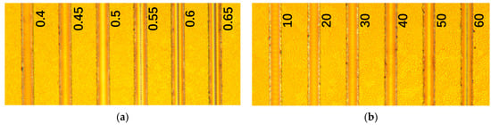
Figure 3.
(a) Micrograph of the ablated area with different P2 laser power (W). (b) Micrograph of the ablated area with different P2 laser repetition frequency (KHz). The power of the laser used is controlled at 0.5 W.
Table 2.
Module performance parameters.
After completing the commissioning of the laser energy, the second step was to adjust the laser P2 repetition frequency. The repetition frequency is the number of pulses of the laser output per unit of time, such as the output of 10 pulses per second laser pulse repetition frequency that is 10 Hz. The greater the laser repetition frequency, the higher the overlap rate of each spot, and the more it tends to form a straight line, while the smaller the repetition frequency, the laser will become a separate spot connected to an ablation line. The lower the repetition frequency, the more the laser becomes a single spot connected to a scribing area. The laser repetition frequency affects the scribing depth and quality, and ultimately the series resistance and open-circuit voltage of the cell. We controlled the power of the laser at 0.5 W, then adjusted the repetition frequency of the laser. As shown in Figure 3b, it was found that as the laser repetition frequency increases, the P2 ablation area becomes cleaner, but due to the thermal effect of the laser, ablation marks appear at the edges of P2, resulting in discontinuity of the top Au electrode evaporated at the edges of P2 and increasing the transmission resistance. The P2 ablated area has the best morphology when the repetition frequency was kept at 20–30 KHz.
After the laser energy and repetition frequency are adjusted to a suitable range, we need to optimize the dead width. For the laser, whether it is a square cavity mirror or a circular cavity mirror, the light intensity distribution in the cross-sectional plane is a circular spot with the strongest light intensity in the center and gradually decreases in the direction of the edges in a Gaussian type of distribution. Since the laser is a Gaussian beam with higher energy at the center and lower energy at the edges, there will be some residues of reactants at the edges due to the weaker energy at the edges, although the perovskite is completely removed at the center when the P2 laser is ablated. As shown in Figure 4a, at the plate thickness setting of 3 cm, the P2 width is 80 μm, and the center part of the scribing area is yellow (ITO color is yellow), indicating that the laser removed all the substances from the upper layer of ITO. The ablated area at the edge shows a purple color, which indicates that the material on the ITO layer was not removed cleanly, and black residues can clearly be seen in the ablated area, as shown in the red box in Figure 4a. We performed XRD characterization of the black residue in the P2 ablated area, as shown in Figure 5. Comparing the XRD spectra of the perovskite film and the P2 residue, we find that the XRD diffraction peaks of the P2 residue are mainly those of PbI2, with only a small portion of perovskite. This indicates that under the action of the P2 laser, the perovskite decomposed and a large amount of PbI2 crystals were produced. These PbI2 crystals can cause poor contact between the top metal electrode and the bottom ITO electrode and can affect the stability of the module. Therefore, we need to optimize the P2 laser process to remove this part of the residue at the edge of the P2 scribing area.
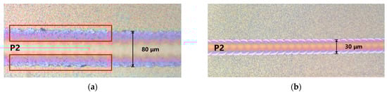
Figure 4.
(a) 80 μm width laser P2 ablation area; (b) 30 μm width laser P2 ablated area.
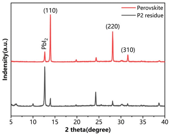
Figure 5.
XRD patterns of perovskite film and P2 residue.
Controlling other conditions constant, we increase the distance between the substrate and the laser exit, so that the focus of the laser moves upward relative to the film, which eventually reduces the laser spot on the film, thus reducing the width of the P2 laser and making the laser energy more concentrated to reduce the residual PbI2 at the edges. This method not only reduces the residual P2 scribing edges but also significantly reduces the P2 width and reduces the dead area. As shown in Figure 4b, the residual PbI2 in the P2 ablated region was effectively removed and the P2 ablated region has a better morphology, while the width of P2 was significantly reduced from 80 μm to about 30 μm.
Table 3 shows the P2 widths obtained by varying the laser depth of focus (i.e., the distance between the laser exit and the substrate) while keeping other conditions the same. For the experimental setup we used a dual optical path laser scribing machine from Shenzhen Kyowa Intelligent Technology Co., Ltd. which has a minimum scribing width of 30 microns. Due to the limitation of the instrument, it was difficult to reduce the P2 width below 30 μm, which was the narrowest width that can be achieved without affecting the carrier transmission.
Table 3.
P2 ablation width versus laser depth of focus.
2.3. P3 Laser Process
The role of P3 is mainly to isolate the metal electrodes on the top of the module and realize the series connection of each cell. An incorrect form of P3 laser scribing can lead to (1) difficulty in removing the Ag electrodes from the surface, resulting in their residual in the ablated area, and (2) prolonged laser ablation, which can cause localized heating and lead to damage to the perovskite layer between adjacent sub-cells. Incomplete Ag removal may create a short circuit between the top electrodes of two adjacent sub-cells. The presence of a small amount of Ag flakes in the P3 ablation area may lead to the formation of a current path, resulting in an electrical connection between adjacent cells, and ultimately damaging the performance of the module. There are two process routes for P3—the first of which the laser is incident from the glass surface and removes all layers on the ITO, including the SnO2 layer, the perovskite layer, the HTL layer, and the metal electrode layer, to form a complete P3 ablated area, called the back-side P3 process.; and the second method being the front-side laser process, in which the laser is incident from the metal electrode surface and removes only the metal electrode layer on the surface, thus achieving electrical isolation.
The back-side laser P3 process is easy to achieve because the perovskite layer has a high absorption rate of laser light and can absorb energy and vaporize at a lower laser energy, thus taking away the metal electrodes on its upper layer and realizing the series connection between subunits in the module, as shown in Figure 6a. The process of realizing the backside laser is relatively simple, but there is a big problem concerning the Ag electrode will be torn, as shown in the red dotted circle in Figure 6a. Since Ag electrodes are carried away by functional layers such as vaporized perovskite and do not directly absorb laser energy, coupled with the fact that Ag has good ductility, the removal of Ag in the P3 scribing region will inevitably result in the surrounding Ag electrode layers being brought up together and off the surface of the spiro-OMeTAD, forming a tear-like crater structure. This results in the formation of a large amount of Ag debris at the edge or inside the P3 scribing area, which has a high probability of being distributed to form current paths within the P3 scribing area. Furthermore, this tearing of Ag electrodes may lead to the destruction of Ag within P2, resulting in poor contact between the top and bottom electrodes, leading to difficult charge transfer and increased series resistance.
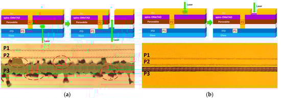
Figure 6.
(a) Reverse laser P3 ablation schematic and actual results. (b) Frontal laser P3 ablation schematic and actual results.
To solve the problems of P3 tearing and controlling the dead area width, we conducted a study of frontal P3. As shown in Figure 6b, the frontal P3 process uses a laser incident from the Ag electrode to remove the Ag electrode in the P3 ablated area. Since most of the laser light is reflected or absorbed by the Ag electrode layer, the other functional layers in the P3 ablated area are retained. Since functional layers such as perovskite and spiro-OMeTAD can only transmit charge in almost vertical directions, they do not affect the effect of P3. The advantage of front-side P3 is the simplicity of the process, as well as the ability to greatly reduce the area of dead areas. As shown in Figure 6, the front-side P3 laser process can greatly improve the quality of the ablation, while comparing the effect of front-side and back-side P3, it is found that using front-side P3 can greatly reduce the width of the dead area, which is reflected in the significant improvement of JSC in the module.
The final P4 edge clearing process uses a 1064 nm infrared laser to clear all areas other than the active area of the cell and the sink bar area, including all layers between the ITO and Au electrodes, leaving only the glass substrate, as shown in Figure 2a, the blue area is the edge clearing area. After the completion of edge clearing, the complete module can be formed by pasting the sink bar in the yellow sink bar area as in Figure 2a.
As shown in Figure 7a, after the laser optimization of P1–P3, the dead area width of the module is significantly reduced, from greater than 150 μm at the beginning to about 70 μm at present, and the GFF value is increased to 99%, which is a world-leading level. Correspondingly, the module short-circuit current density JSC also has a large increase, and the module efficiency has improved significantly, as shown in Figure 7b. The reduction in the dead area means an increase in the active area of the cell, which is manifested in the PV parameters by the significant increase in the short-circuit current density JSC, which is significant. After laser P1, P2, and P3 scribing optimization, we prepared a module with an aperture area of 12.6 cm2, the optimal device open-circuit voltage (VOC), short-circuit current density (JSC), fill factor (FF), and photoelectric conversion efficiency (PCE) were 7.03 V, 4.23 mA/cm2, 76.22%, and 22.69%, respectively, and the J-V curves of the module are shown in Figure 8a. The high efficiency is mainly attributed to the extremely high geometric fill factor (GFF > 99%), which is mainly due to our optimization of the laser process.
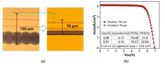
Figure 7.
(a) Change in dead width before and after laser process optimization. (b) Module J-V curves and PV performance parameters before and after laser process optimization.
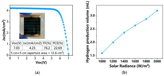
Figure 8.
(a) Optimal device parameters and J-V curve. (b) Hydrogen production from perovskite solar modules as a power source driving electrolytic water production at different solar irradiances.
The electrocatalytic experimental results and electrolytic water hydrogen production effect of the PSMs are shown in Figure 8b. We connected the positive and negative electrodes of the perovskite solar modules to two graphite electrodes and put the graphite electrodes into the electrolyte. Then the light intensity of the xenon lamp was adjusted to simulate sunlight and shine onto the surface of the perovskite solar modules; thus, generating an electric current to electrolyze water for hydrogen production. The rate of hydrogen production was controlled by adjusting the solar irradiance of the xenon lamp, after 5 min of simulated light exposure and then quantitatively analyzed by gas chromatography to obtain six sets of data, as shown in Figure 8b. Table 4 shows the variation of the component VOC and JSC for different solar irradiance. As the solar irradiance rises, the JSC component of the modules increases, causing the volume of hydrogen produced by the electrolysis of water to rise gradually and the overall data to increase linearly. This result indicates that using PSCs as a catalyst for the electrolysis of water is feasible and that hydrogen production from photovoltaic power is a technology that can be expected.
Table 4.
VOC and JSC of perovskite solar modules at different solar irradiance.
3. Materials and Methods
3.1. Materials
Formamide iodide (FAI), rubidium chloride (RbCl), potassium chloride (KCl), and lithium bis(trifluoromethanesulfonyl)imide (Li-TFSI) were purchased from Xi’an, China Xi’an Baolite Optoelectronic Components Co. Methylamine iodide (MAI), methylamine chloride (MABr), cesium iodide (CsI), and lead iodide (PbI2) were purchased from Xi’an Yilante New Material Co. from Xi’an, China. All other materials, including ethanol (EtOH), 2-propanol (IPA), acetone, dimethylformamide (DMF), dimethyl sulfoxide (DMSO), acetonitrile (ACN), chlorobenzene (CB), tert-butylpyridine (tBP), and toluene, were purchased from Shanghai Maclean Biochemical Technology Co. from Shanghai, China. All materials were used as is unless otherwise stated.
3.2. Fabrication of Perovskite Solar Modules (PSMs)
In this work, an ITO glass with a square resistance of 15 Ω/cm2, a thickness of 1.1 cm, and an area of 5 × 5 cm2 was used as the substrate. Firstly, the bottom electrode pattern of the cell was planned using laser cutting P1 to insulate the bottom electrodes of adjacent sub-cells. Then, the ITO glass, after P1 scribing, was ultrasonically cleaned for 20 min in the order of pure water, acetone, isopropanol, and anhydrous ethanol, respectively, and then spin-coated to prepare the electron transport layer after nitrogen blowing and UV ozone treatment for 20 min (the aqueous SnO2 colloidal solution was diluted with pure water at 1:3). The SnO2 solution was subjected to a spin-coating step of 4000 rpm, 20 s, followed by 180 °C, and 20 min annealing. The annealed substrate was treated with UV ozone and then taken into a glove box for spin-coating to prepare the PbI2 layer (PbI2 dissolved in DMF/DMSO at a concentration of 691.5 mg/mL in a volume ratio of 9:1). After spin-coating, the PbI2 films were heated on a hot table at 70 °C for 10 s. After heating, the FA/MA mixture solution (FAI:MAI:MACl = 90:6:12 mg/mL dissolved in IPA) was dropped onto the PbI2 films and spin-coated to form a film, followed by annealing at 150 °C for 15 min in an air atmosphere to promote the formation of perovskite crystals. Afterward, the hole transport layer spiro-OMeTAD was spin-coated (spiro-OMeTAD 72.3 mg/mL dissolved in CB/tBP/Li-TFSI acetonitrile). After the preparation of hole transport layers, laser P2 scribing was performed to selectively remove all film layers between adjacent subunits except ITO to allow them to form a series connection by subsequent deposition of the top electrode. Then, 150 nm thick Au was vaporized as the top electrode in a high vacuum chamber (<10−5 Pa) after P2 scribing was completed, and laser P3 scribing was performed to separate the top electrode just achieved so that the top electrodes of each subunit are separated from each other. Finally, the edge of the cell was removed by laser P4 scribing, and the sink strip was applied to obtain a complete module.
3.3. Characterization Methods and Instruments
The current-voltage curve of the PSMs was measured with a source meter (Keithley B2901A) at AM 1.5, 100 mW/cm2. AM 1.5G simulated solar illumination was provided by a AAA solar simulator (Enli Tech, SS-F5-3A, Taiwan) calibrated by a KG-5 standard silicon cell. X-ray diffraction patterns were collected at room temperature using an X-ray diffractometer (PANalytical B.V., X’Pert Pro MPD) using Cu Kα radiation (λ = 1.5418 Å). The electrodes we used in the process of hydrogen production by electrolysis of water were two graphite electrodes and the electrolyte was a potassium chloride (KCl) solution. The xenon lamp model was the PLS-SXE300/300UV of the PerfectLight.
4. Conclusions
In this paper, we explore the application of the picosecond laser process in the module preparation process based on the two-step preparation of perovskite solar cells with optimized dead area width. The laser process is currently the optimal solution to achieve large areas of perovskite solar cells with fast processing speed, high precision, and low process cost. Through the selection of the P1 laser and the optimization of the P2 and P3 laser processes, the high-efficiency perovskite solar modules were successfully prepared, while the optimization of the dead area width was completed in the process, and the dead area width was reduced from 150 μm to about 70 μm. The optimized laser process finally achieved high GFF (> 99%) and high-efficiency module, and the loss from the small cell (24%) to the module (22.69%) was only about 1.3%, which proves that the optimized laser process is an effective way to achieve high GFF (> 99%) and high-efficiency module. By testing the experiment of hydrogen production from electrolytic water, we proved the feasibility of hydrogen production from photovoltaic power, but the specific energy conversion efficiency and the possible problems in the practical application need to be further studied.
Author Contributions
Conceptualization, L.Y., W.Z., G.Y., W.Y. and Y.H.; data curation, L.Y., W.Z., H.G., G.Y., Y.D. and L.Z.; investigation, L.Y., W.Z., W.Y., Y.D. and W.L.; methodology, L.Y., W.Z., G.Y., W.Y. and Y.H.; resources, H.G., W.Y., Y.D., L.Z. and W.L.; writing—original draft, L.Y. and W.Z.; writing—review and editing, L.Y. and W.Z. All authors have read and agreed to the published version of the manuscript.
Funding
This work was supported by the Sichuan Science and Technology Program (2022YFSY0040, 2022NSFSC0306) and the Production-Education Integration Demonstration Project of Sichuan Province “Photovoltaic Industry Production-Education Integration Comprehensive Demonstration Base of Sichuan Province (Sichuan Financial Education [2022] No.106)”.
Data Availability Statement
No new data were created or analyzed in this study. Data sharing is not applicable to this article.
Conflicts of Interest
The authors declare no conflict of interest.
References
- Ding, Y.; Ding, B.; Kanda, H.; Usiobo, O.J.; Gallet, T.; Yang, Z.; Liu, Y.; Huang, H.; Sheng, J.; Liu, C.; et al. Single-Crystalline TiO2 Nanoparticles for Stable and Efficient Perovskite Modules. Nat. Nanotechnol. 2022, 17, 598–605. [Google Scholar] [CrossRef]
- Li, X.; Zhang, W.; Guo, X.; Lu, C.; Wei, J.; Fang, J. Constructing Heterojunctions by Surface Sulfidation for Efficient Inverted Perovskite Solar Cells. Science 2022, 375, 434–437. [Google Scholar] [CrossRef] [PubMed]
- Zhao, Y.; Ma, F.; Qu, Z.; Yu, S.; Shen, T.; Deng, H.-X.; Chu, X.; Peng, X.; Yuan, Y.; Zhang, X.; et al. Inactive (PbI2)2 RbCl Stabilizes Perovskite Films for Efficient Solar Cells. Science 2022, 377, 531–534. [Google Scholar] [CrossRef] [PubMed]
- Li, Y.; Chen, Z.; Yu, B.; Tan, S.; Cui, Y.; Wu, H.; Luo, Y.; Shi, J.; Li, D.; Meng, Q. Efficient, Stable Formamidinium-Cesium Perovskite Solar Cells and Minimodules Enabled by Crystallization Regulation. Joule 2022, 6, 676–689. [Google Scholar] [CrossRef]
- You, S.; Zeng, H.; Liu, Y.; Han, B.; Li, M.; Li, L.; Zheng, X.; Guo, R.; Luo, L.; Li, Z.; et al. Radical Polymeric P-Doping and Grain Modulation for Stable, Efficient Perovskite Solar Modules. Science 2023, 379, 288–294. [Google Scholar] [CrossRef] [PubMed]
- Gao, D.; Li, B.; Li, Z.; Wu, X.; Zhang, S.; Zhao, D.; Jiang, X.; Zhang, C.; Wang, Y.; Li, Z.; et al. Highly Efficient Flexible Perovskite Solar Cells through Pentylammonium Acetate Modification with Certified Efficiency of 23.35%. Adv. Mater. 2023, 35, 2206387. [Google Scholar] [CrossRef]
- Park, J.; Kim, J.; Yun, H.-S.; Paik, M.J.; Noh, E.; Mun, H.J.; Kim, M.G.; Shin, T.J.; Seok, S.I. Controlled Growth of Perovskite Layers with Volatile Alkylammonium Chlorides. Nature 2023, 616, 724–730. [Google Scholar] [CrossRef]
- Yang, L.; Zhou, H.; Duan, Y.; Wu, M.; He, K.; Li, Y.; Xu, D.; Zou, H.; Yang, S.; Fang, Z.; et al. 25.24%-Efficiency FACsPbI3 Perovskite Solar Cells Enabled by Intermolecular Esterification Reaction of DL-Carnitine Hydrochloride. Adv. Mater. 2023, 35, 2211545. [Google Scholar] [CrossRef] [PubMed]
- Bu, T.; Ono, L.K.; Li, J.; Su, J.; Tong, G.; Zhang, W.; Liu, Y.; Zhang, J.; Chang, J.; Kazaoui, S.; et al. Modulating Crystal Growth of Formamidinium–Caesium Perovskites for over 200 cm2 Photovoltaic Sub-Modules. Nat. Energy 2022, 7, 528–536. [Google Scholar] [CrossRef]
- Yang, Z.; Liu, Z.; Ahmadi, V.; Chen, W.; Qi, Y. Recent Progress on Metal Halide Perovskite Solar Minimodules. Solar RRL 2022, 6, 2100458. [Google Scholar] [CrossRef]
- Chiang, C.-H.; Wu, C.-G. Large-Area Perovskite Film Prepared by New FFASE Method for Stable Solar Modules Having High Efficiency under Both Outdoor and Indoor Light Harvesting. Adv. Sci. 2023, 10, 2205967. [Google Scholar] [CrossRef] [PubMed]
- Guo, R.; Zhang, X.; Zheng, X.; Li, L.; Li, M.; Zhao, Y.; Zhang, S.; Luo, L.; You, S.; Li, W.; et al. Tailoring Multifunctional Self-Assembled Hole Transporting Molecules for Highly Efficient and Stable Inverted Perovskite Solar Cells. Adv. Funct. Mater. 2023, 33, 2211955. [Google Scholar] [CrossRef]
- Tan, L.; Zhou, J.; Zhao, X.; Wang, S.; Li, M.; Jiang, C.; Li, H.; Zhang, Y.; Ye, Y.; Tress, W.; et al. Combined Vacuum Evaporation and Solution Process for High-Efficiency Large-Area Perovskite Solar Cells with Exceptional Reproducibility. Adv. Mater. 2023, 35, 2205027. [Google Scholar] [CrossRef]
- Cheng, Y.; Peng, Y.; Jen, A.K.-Y.; Yip, H.-L. Development and Challenges of Metal Halide Perovskite Solar Modules. Solar RRL 2022, 6, 2100545. [Google Scholar] [CrossRef]
- Yoon, J.-H.; Park, J.-K.; Kim, W.M.; Lee, J.; Pak, H.; Jeong, J. Characterization of Efficiency-Limiting Resistance Losses in Monolithically Integrated Cu(In,Ga)Se2 Solar Modules. Sci. Rep. 2015, 5, 7690. [Google Scholar] [CrossRef]
- Li, Z.; Klein, T.R.; Kim, D.H.; Yang, M.; Berry, J.J.; van Hest, M.F.A.M.; Zhu, K. Scalable Fabrication of Perovskite Solar Cells. Nat. Rev. Mater. 2018, 3, 18017. [Google Scholar] [CrossRef]
- Bu, T.; Li, J.; Li, H.; Tian, C.; Su, J.; Tong, G.; Ono, L.K.; Wang, C.; Lin, Z.; Chai, N.; et al. Lead Halide—Templated Crystallization of Methylamine-Free Perovskite for Efficient Photovoltaic Modules. Science 2021, 372, 1327–1332. [Google Scholar] [CrossRef] [PubMed]
- Yang, Z.; Zhang, W.; Wu, S.; Zhu, H.; Liu, Z.; Liu, Z.; Jiang, Z.; Chen, R.; Zhou, J.; Lu, Q.; et al. Slot-Die Coating Large-Area Formamidinium-Cesium Perovskite Film for Efficient and Stable Parallel Solar Module. Sci. Adv. 2021, 7, eabg3749. [Google Scholar] [CrossRef]
- Shalan, A.E. Challenges and Approaches towards Upscaling the Assembly of Hybrid Perovskite Solar Cells. Mater. Adv. 2020, 1, 292–309. [Google Scholar] [CrossRef]
- Rong, Y.; Ming, Y.; Ji, W.; Li, D.; Mei, A.; Hu, Y.; Han, H. Toward Industrial-Scale Production of Perovskite Solar Cells: Screen Printing, Slot-Die Coating, and Emerging Techniques. J. Phys. Chem. Lett. 2018, 9, 2707–2713. [Google Scholar] [CrossRef]
- Razza, S.; Pescetelli, S.; Agresti, A.; Di Carlo, A. Laser Processing Optimization for Large-Area Perovskite Solar Modules. Energies 2021, 14, 1069. [Google Scholar] [CrossRef]
- Di Giacomo, F.; Castriotta, L.A.; Kosasih, F.U.; Di Girolamo, D.; Ducati, C.; Di Carlo, A. Upscaling Inverted Perovskite Solar Cells: Optimization of Laser Scribing for Highly Efficient Mini-Modules. Micromachines 2020, 11, 1127. [Google Scholar] [CrossRef] [PubMed]
- Fenske, M.; Schultz, C.; Dagar, J.; Kosasih, F.U.; Zeiser, A.; Junghans, C.; Bartelt, A.; Ducati, C.; Schlatmann, R.; Unger, E.; et al. Improved Electrical Performance of Perovskite Photovoltaic Mini-Modules through Controlled PbI 2 Formation Using Nanosecond Laser Pulses for P3 Patterning. Energy Tech. 2021, 9, 2000969. [Google Scholar] [CrossRef]
- Yang, M.; Kim, D.H.; Klein, T.R.; Li, Z.; Reese, M.O.; Tremolet de Villers, B.J.; Berry, J.J.; van Hest, M.F.A.M.; Zhu, K. Highly Efficient Perovskite Solar Modules by Scalable Fabrication and Interconnection Optimization. ACS Energy Lett. 2018, 3, 322–328. [Google Scholar] [CrossRef]
- Qiu, L.; Liu, Z.; Ono, L.K.; Jiang, Y.; Son, D.; Hawash, Z.; He, S.; Qi, Y. Scalable Fabrication of Stable High Efficiency Perovskite Solar Cells and Modules Utilizing Room Temperature Sputtered SnO2 Electron Transport Layer. Adv. Funct. Mater. 2019, 29, 1806779. [Google Scholar] [CrossRef]
- Liu, Z.; Qiu, L.; Ono, L.K.; He, S.; Hu, Z.; Jiang, M.; Tong, G.; Wu, Z.; Jiang, Y.; Son, D.-Y.; et al. A Holistic Approach to Interface Stabilization for Efficient Perovskite Solar Modules with over 2,000-Hour Operational Stability. Nat. Energy 2020, 5, 596–604. [Google Scholar] [CrossRef]
- Yaghoobi Nia, N.; Lamanna, E.; Zendehdel, M.; Palma, A.L.; Zurlo, F.; Castriotta, L.A.; Di Carlo, A. Doping Strategy for Efficient and Stable Triple Cation Hybrid Perovskite Solar Cells and Module Based on Poly(3-hexylthiophene) Hole Transport Layer. Small 2019, 15, 1904399. [Google Scholar] [CrossRef]
- Park, N.-G.; Zhu, K. Scalable Fabrication and Coating Methods for Perovskite Solar Cells and Solar Modules. Nat. Rev. Mater. 2020, 5, 333–350. [Google Scholar] [CrossRef]
- Dai, X.; Chen, S.; Jiao, H.; Zhao, L.; Wang, K.; Ni, Z.; Yu, Z.; Chen, B.; Gao, Y.; Huang, J. Efficient Monolithic All-Perovskite Tandem Solar Modules with Small Cell-to-Module Derate. Nat. Energy 2022, 7, 923–931. [Google Scholar] [CrossRef]
- Wang, X.; Liu, D.; Liu, R.; Du, X.; Zhang, B.; Sun, X.; Chen, C.; Li, Z.; Zhao, Q.; Shao, Z.; et al. PbI6 Octahedra Stabilization Strategy Based on π-π Stacking Small Molecule Toward Highly Efficient and Stable Perovskite Solar Cells. Adv. Energy Mater. 2023, 13, 2203635. [Google Scholar] [CrossRef]
- Abdin, Z.; Zafaranloo, A.; Rafiee, A.; Mérida, W.; Lipiński, W.; Khalilpour, K.R. Hydrogen as an Energy Vector. Renew. Sustain. Energy Rev. 2020, 120, 109620. [Google Scholar] [CrossRef]
- Liu, B.; Feng, S.; Yang, L.; Li, C.; Luo, Z.; Wang, T.; Gong, J. Bifacial Passivation of N-Silicon Metal–Insulator–Semiconductor Photoelectrodes for Efficient Oxygen and Hydrogen Evolution Reactions. Energy Environ. Sci. 2020, 13, 221–228. [Google Scholar] [CrossRef]
- Ouyang, T.; Hu, X.; Liu, W.; Shi, X.; Lu, J. An Innovative Model for Biofilm-Based Microfluidic Microbial Fuel Cells. J. Power Sources 2022, 521, 230940. [Google Scholar] [CrossRef]
- Divekar, A.G.; Gerhardt, M.R.; Antunes, C.M.; Osmieri, L.; Yang-Neyerlin, A.C.; Weber, A.Z.; Pivovar, B.S.; Bender, G.; Herring, A.M. Spatially Resolved Performance and Degradation in a Perfluorinated Anion Exchange Membrane Fuel Cell. Electrochim. Acta 2022, 406, 139812. [Google Scholar] [CrossRef]
- Razza, S.; Di Giacomo, F.; Matteocci, F.; Cinà, L.; Palma, A.L.; Casaluci, S.; Cameron, P.; D’Epifanio, A.; Licoccia, S.; Reale, A.; et al. Perovskite Solar Cells and Large Area Modules (100 cm2) Based on an Air Flow-Assisted PbI2 Blade Coating Deposition Process. J. Power Sources 2015, 277, 286–291. [Google Scholar] [CrossRef]
- Agresti, A.; Pescetelli, S.; Palma, A.L.; Del Rio Castillo, A.E.; Konios, D.; Kakavelakis, G.; Razza, S.; Cinà, L.; Kymakis, E.; Bonaccorso, F.; et al. Graphene Interface Engineering for Perovskite Solar Modules: 12.6% Power Conversion Efficiency over 50 cm2 Active Area. ACS Energy Lett. 2017, 2, 279–287. [Google Scholar] [CrossRef]
- Du, M.; Zhu, X.; Wang, L.; Wang, H.; Feng, J.; Jiang, X.; Cao, Y.; Sun, Y.; Duan, L.; Jiao, Y.; et al. High-Pressure Nitrogen-Extraction and Effective Passivation to Attain Highest Large-Area Perovskite Solar Module Efficiency. Adv. Mater. 2020, 32, 2004979. [Google Scholar] [CrossRef] [PubMed]
- Green, M.A.; Dunlop, E.D.; Hohl-Ebinger, J.; Yoshita, M.; Kopidakis, N.; Hao, X. Solar Cell Efficiency Tables (Version 58). Prog. Photovolt. Res. Appl. 2021, 29, 657–667. [Google Scholar] [CrossRef]
- Moon, S.-J.; Yum, J.-H.; Löfgren, L.; Walter, A.; Sansonnens, L.; Benkhaira, M.; Nicolay, S.; Bailat, J.; Ballif, C. Laser-Scribing Patterning for the Production of Organometallic Halide Perovskite Solar Modules. IEEE J. Photovolt. 2015, 5, 1087–1092. [Google Scholar] [CrossRef]
- Liu, C.; Yang, Y.; Rakstys, K.; Mahata, A.; Franckevicius, M.; Mosconi, E.; Skackauskaite, R.; Ding, B.; Brooks, K.G.; Usiobo, O.J.; et al. Tuning Structural Isomers of Phenylenediammonium to Afford Efficient and Stable Perovskite Solar Cells and Modules. Nat. Commun. 2021, 12, 6394. [Google Scholar] [CrossRef]
- Yoo, J.W.; Jang, J.; Kim, U.; Lee, Y.; Ji, S.-G.; Noh, E.; Hong, S.; Choi, M.; Seok, S.I. Efficient Perovskite Solar Mini-Modules Fabricated via Bar-Coating Using 2-Methoxyethanol-Based Formamidinium Lead Tri-Iodide Precursor Solution. Joule 2021, 5, 2420–2436. [Google Scholar] [CrossRef]
- Abdollahi Nejand, B.; Ritzer, D.B.; Hu, H.; Schackmar, F.; Moghadamzadeh, S.; Feeney, T.; Singh, R.; Laufer, F.; Schmager, R.; Azmi, R.; et al. Scalable Two-Terminal All-Perovskite Tandem Solar Modules with a 19.1% Efficiency. Nat. Energy 2022, 7, 620–630. [Google Scholar] [CrossRef]
- Gao, Y.; Liu, C.; Xie, Y.; Guo, R.; Zhong, X.; Ju, H.; Qin, L.; Jia, P.; Wu, S.; Schropp, R.E.I.; et al. Can Nanosecond Laser Achieve High-Performance Perovskite Solar Modules with Aperture Area Efficiency Over 21%? Adv. Energy Mater. 2022, 12, 2202287. [Google Scholar] [CrossRef]
Disclaimer/Publisher’s Note: The statements, opinions and data contained in all publications are solely those of the individual author(s) and contributor(s) and not of MDPI and/or the editor(s). MDPI and/or the editor(s) disclaim responsibility for any injury to people or property resulting from any ideas, methods, instructions or products referred to in the content. |
© 2023 by the authors. Licensee MDPI, Basel, Switzerland. This article is an open access article distributed under the terms and conditions of the Creative Commons Attribution (CC BY) license (https://creativecommons.org/licenses/by/4.0/).