Article

Single-Layer MoS2-MoO3-x Heterojunction Nanosheets with Simultaneous Photoluminescence and Co-Photocatalytic Features

1
Department of Physics, Institute for Advanced Studies in Basic Sciences (IASBS), Zanjan 45137-66731, Iran
2
Department of Physics, Sharif University of Technology, P.O. Box 11155-9161, Tehran, Iran
*
Author to whom correspondence should be addressed.
Catalysts 2021, 11(12), 1445; https://doi.org/10.3390/catal11121445
Submission received: 25 October 2021 / Revised: 18 November 2021 / Accepted: 24 November 2021 / Published: 27 November 2021

Abstract

:
Single-layer MoS2-MoO3-x heterojunction nanosheets with visible-light-sensitive band gap energy and average lateral dimensions of ~70 nm were synthesized by using a two-step combined exfoliation method. The exfoliation was initiated from pristine MoS2, while some sulfur sites in expanded MoS2 sheets during exfoliating were substituted by ambient non-thermal oxygen, resulting in formation of α-MoO3-x crystalline domains. The morphological features, crystalline structure, phase formation, number of layers, and optical properties of the MoS2-MoO3-x nanosheets were determined by atomic force microscopy; X-ray diffraction; field emission electron microscopy; transmission electron microscopy; and Raman, UV–visible–NIR, diffuse transmittance, and photoluminescence spectroscopies. The produced α-MoO3-x domains displayed a narrower indirect band gap energy (~1.95 eV) than that of stoichiometric MoO3 (~3 eV), and a broad light absorption range from visible to near-infrared region can act as a plasmonic material facilitating the separation of the photoinduced carriers and enhancing the photocatalytic activity of the MoS2 domain, having ~1.75(2.16) eV indirect (direct) band gap energy. In this regard, the MoS2-MoO3-x heterojunction nanosheets showed single-layer-based excitation-dependent luminescence emissions and visible-light-induced photocatalytic features, at the same time. This study can contribute to promising applications of sheet-like nanomaterials for purposes requiring simultaneous photoluminescence and photocatalytic features, such as in-vivo monitoring and targeting.

Graphical Abstract

1. Introduction

Photocatalytic materials have attracted increasing attention in various scientific fields [1] and for various technological applications [2,3] since 1972 [4]. In response to the growth of environmental pollutants and infections, photocatalysts can be widely used in environmental remediation processes such as organic pollutants decomposition [4,5]; inorganic pollutant treatment [5]; photocatalytic disinfection of bacteria [5,6], viruses [7], and parasitic organisms [8]; and photocatalytic hydrogen production for replacing fossil fuels [9,10,11]. TiO2 [12] and ZnO [13], as efficient photocatalysts, are mostly applicable in common processes, but TiO2’s wide band gap in pure state (~3.2 eV) is considered a barrier to its use due to having an excitation wavelength in the UV region [5]. This problem can be overcome by addition and/or cooperation of metallic [14] or carbon-based [15] nanomaterials. Recently, MoS2 nanosheets have been applied as effective photocatalysts (the fewer layers, the higher the photocatalytic activity [5]), because of their excellent optical and chemical properties [5,16,17] and having a more suitable and direct band gap energy of about 1.9 eV in single-layer MoS2 for harvesting visible light than the bulk MoS2, which has a small and insufficient indirect band gap (1.2 eV) [5], large surface area [18], and high in-plane carrier mobility (200–500 cm2/V s) in single-layer MoS2 [16,19]. MoS2 is earth-abundant and non-toxic for environmental application [4,5]. In photocatalytic processes, the existence of MoS2 single layers results in a very high and fast absorption capacity in the visible light region due to direct band gap energy, which is greater than that of MoS2 multilayers with indirect band gap energy [20]. On the other hand, the ultrathin MoS2 nanosheets show higher electron mobility and catalytic activity than bulk MoS2, which is beneficial to transferring photogenerated charges [21,22,23]. The high catalytic activity of ultrathin MoS2 nanosheets (especially 1T-MoS2) is due to the number of active edge sites for catalysis [22,23].
Among various exfoliation methods for bulk MoS2, liquid-phase chemical exfoliation approaches for the production of MoS2 single layers (as the nanosheets with the highest photocatalytic activity [5]) are highly attractive due to very good control of the amount of intercalated atoms [24], the high yield of MoS2 single layers, cost-effectiveness, and mass scalability [16,19,25]. The liquid-phase chemical exfoliation based on the intercalation of alkali metals such as Li and Na results in the partial loss of semiconducting 2H-MoS2 phase [26] due to structural deformation and the change from trigonal prismatic (2H-MoS2, stable semiconductor phase) to octahedral (1T-MoS2, metastable metal phase [16,19,27]. However, 1T-MoS2 phase is unstable, so a heat treatment converts 1T-phase to 2H-phase [16]. It is worth noting, though, that the existence of 1T-MoS2 domains as co-catalyst enhances charge mobility in the material, which causes higher electrochemical and photocatalytic performances [28]. In this regard, Fan et al. [29] prepared 1T@2H-MoS2/black-TiO2 core–shell structures, which were applied as an effective photocatalyst for the degradation of RhB under visible light irradiation.
In pure MoS2 single layers, insufficient photocatalyst separation induces a fast photogenerated electron–hole recombination, causes a low photocatalytic activity, and finally, hinders practical application of pure MoS2 as an efficient photocatalyst [4,30]. Hence, incorporation of other photocatalyst species with appropriate properties is known as one of the effective ways to reduce the recombination efficiency of photoexcited e − h+ pairs [11,29]. In this regard, MoO3-x substoichiometric nanosheets with orthorhombic phase (α-MoO3-x) in corporation with MoS2 single layers can be considered as effective co-photocatalysts, due to their excellent electrochemical, photochemical, and catalytic properties [31,32,33], which arise from the possibility of having a wide range of oxidation states ranging from +2 to +6 owing to the presence of delocalized 4d electrons [32]. The α-MoO3-x possesses a higher photocatalytic activity with narrower band gap energy than stoichiometric MoO3 (with band gap energy of ~2.8–3.6 eV) [10,31,34]. The presence of MoO3-x domains with broad light absorption range inhibits the undesirable electron–hole recombination and promotes the electron–hole separation. Interestingly, the α-MoO3-x phase shows a highly reactive nonmetallic plasmonic property with a strong absorption and localized surface plasmon resonance (LSPR) across the visible to near-infrared region [35,36,37,38]. MoO3-x domains with a large amount of Mo5+ oxidation states enable easy charge carrier generation due to plasmonic effect, so that the integration of MoO3-x as a LSPR material with MoS2 ultrathin nanosheets provides a considerable number of active edge sites for catalysis and enhances the catalytic and light-harvesting performances [22,23,39].
In this regard, Patra et al. [39] prepared a MoS2/MoO3-x/RGO nanocomposite from a MoS2/GO composite by a hydrothermal synthesis followed by calcination under N2 atmosphere, since they could more greatly enhance the photocatalytic activity of MoS2/MoO3-x/RGO nanocomposite than the pristine MoS2/GO composite. Li [30] et al. prepared the α-MoO3@MoS2 hybrid rod–sphere structure via a hydrothermal method and applied it as a photocatalyst with synergistic effects for degradation of organics. Chen et al. [20] synthesized the porous MoO3@MoS2 core–shell nanorods by hydrothermal method using MoO3 nanorod as the precursor for RhB photodegradation. They reported that at a low concentration of RhB, the MoO3@MoS2 sample exhibited photocatalytic degradation ability. However, few studies have been conducted on synthesis, characterization, and photocatalytic activity of MoS2-MoO3-x heterojunction as photocatalyst.
In this study, single-layer MoS2-MoO3-x heterojunction nanosheets were synthesized by using a two-step combined liquid-phase chemical self-exfoliation technique at room temperature. The morphological features, crystalline structure, photoluminescent properties, and optical band gap energy of the separate MoS2 and MoO3-x regions of the heterojunction sheets were examined. The capability of MoS2-MoO3-x heterojunction nanosheets for presenting single-layer-based excitation-dependent luminescence emissions and visible-light-induced photocatalytic features at the same time was investigated. Finally, the mechanism involved in the simultaneous photoluminescence and photocatalytic activity is discussed. It should be clarified that the main goal of this work is indicating the ability to form 2D MoS2-MoO3-x heterojunctions working as a photocatalyst, without any attempt at optimization. However, optimization can be considered in the future works.

2. Results and Discussion

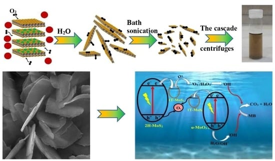
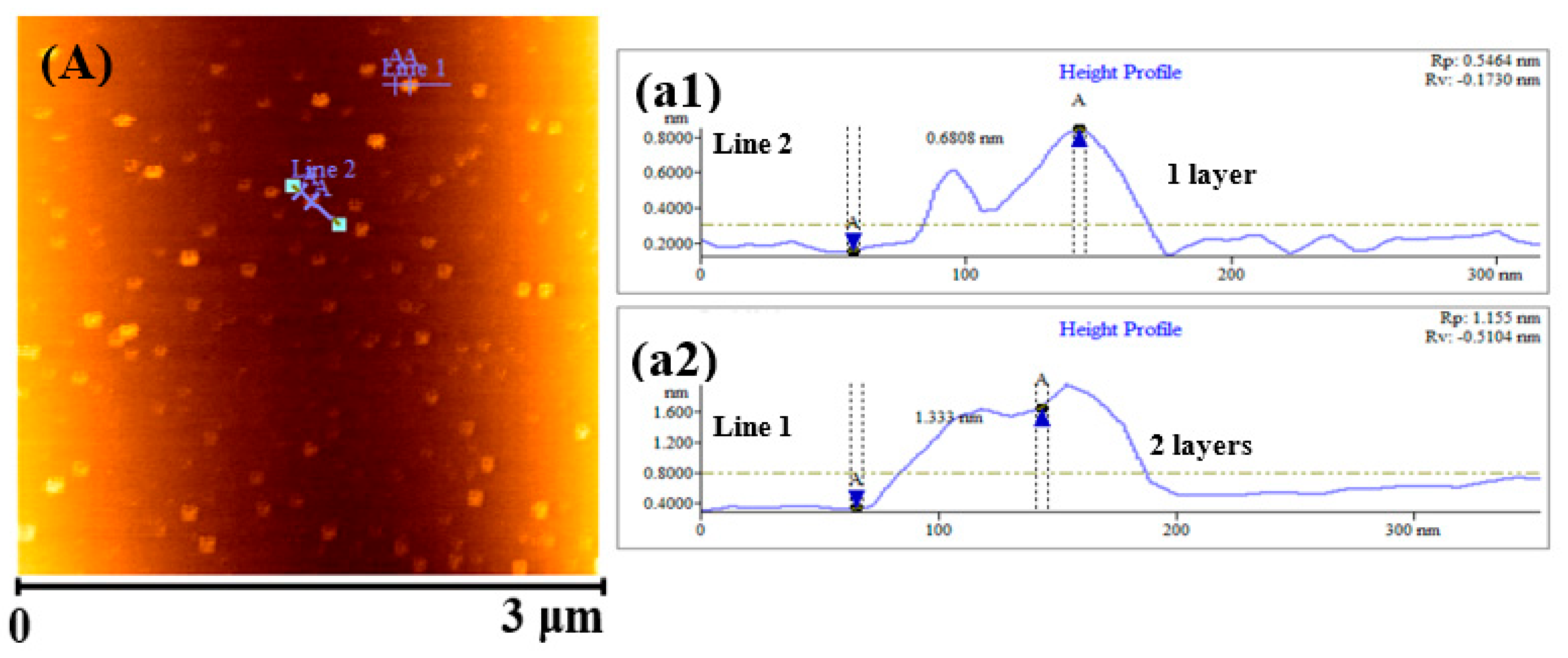
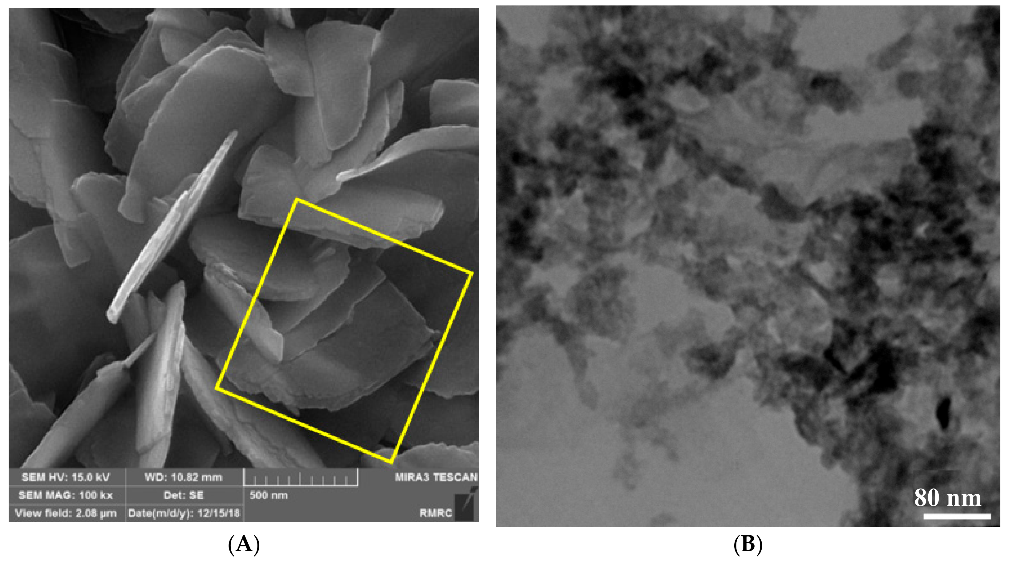
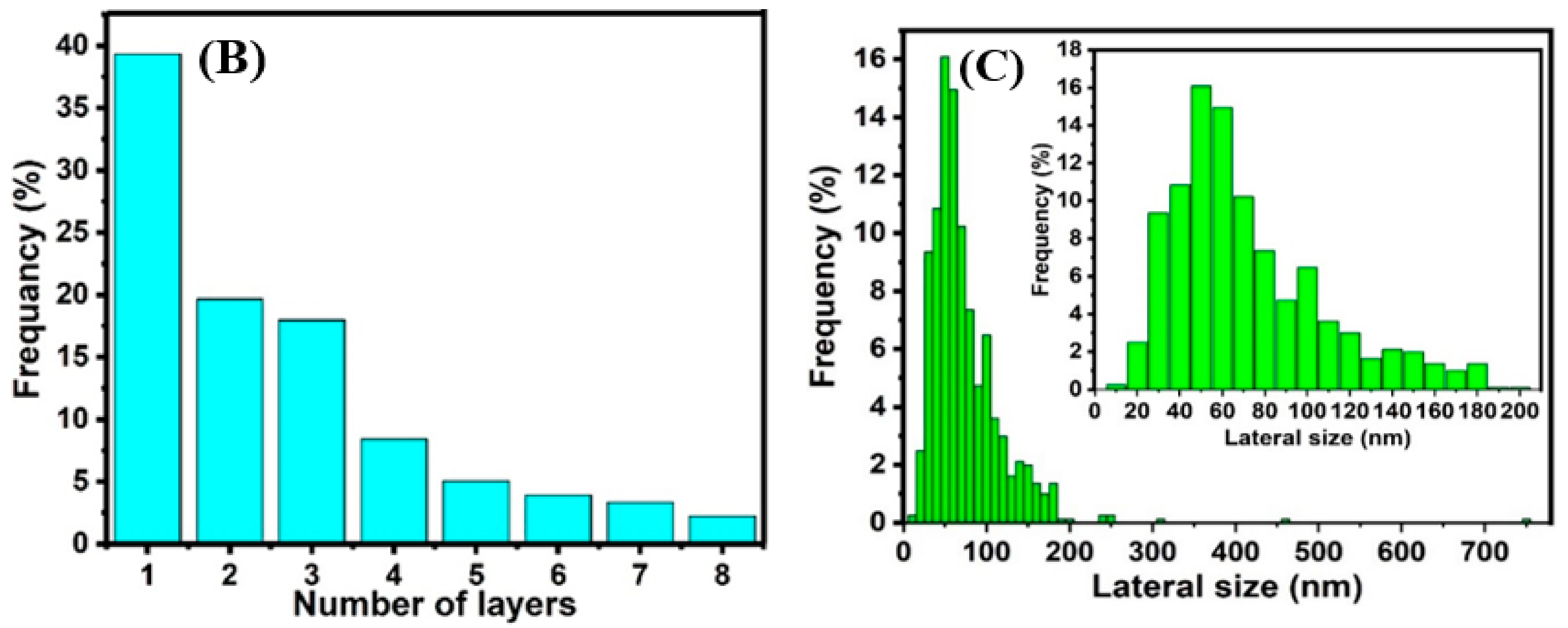
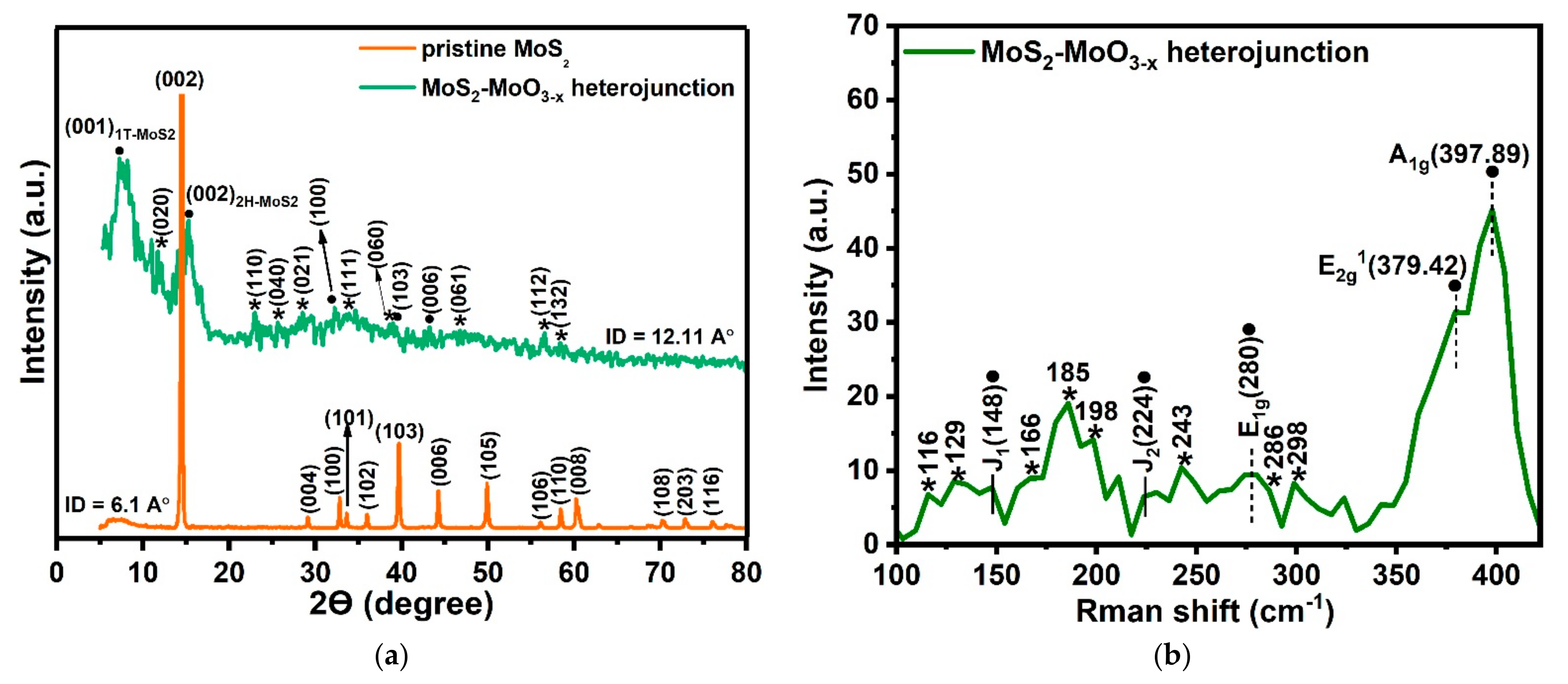
2.1. Structural Analysis

The surface morphology of the synthesized MoS2-MoO3-x heterojunctions were characterized by FESEM and TEM, as presented in Figure 1. In this regard, Figure 1A shows some sheet-like features with large lateral size of ~500 nm, which are often features indicating multi-layers, due to aggregation of the layers during SEM sample preparation. The presence of some structural edge defects and disorder (as marked with yellow rectangular in FESEM image) are distinguishable in the image. It should be noted that our SEM experiences showed that imaging as well as distinguishing the single- and/or multi-layer sheets were very hard. Therefore, for obtaining a SEM image with distinguishable sheet-like features, we selected the aggregated samples (in contrast to the sample preparations considered for AFM and TEM). This means that any condition resulting in aggregation of the sheets can result in the morphologies presented in the SEM image.
In Figure 1B, a better presentation for the unaggregated sheets is given. The more transparent regions can be assigned to the presence of single-layer sheets, and the dark regions are attributed to overlapping of the sheets. The light-brown transparent solution shown in Figure 1C also demonstrated high uniform dispersion and solubility of the sheets in water without any sedimentation.
The morphology, thickness and the lateral dimensions of the sheets were investigated by AFM, as shown in Figure 2. The thickness of single-layer MoS2 or MoO3-x is almost the same at about 0.6–0.7 nm [34,40,41]. In this work, the thickness of the sheets obtained through the height profile analysis was found to be ~0.6–1.0 nm, indicating the presence of single layers in the synthesized samples. The height profiles along the randomly selected colored cross-lines in Figure 2A exhibit single- and bi-layers of the sheets with lateral sizes ~200 nm. The histograms B and C present statistical data of the layer number and lateral size distribution of the sheets, respectively. The average lateral dimension of MoS2-MoO3-x single layers is ~70 nm (histogram C). The MoS2-MoO3-x heterojunctions with lateral size below 100 nm are often single-layer. It should be noted that although the lateral dimension of ~70 nm is not distinguished as a critical size in our work, we tried to reduce the lateral dimension down to values lower than 100 nm, in order to obtain intensive as well as sharp PL peaks. In addition, further reduction in the lateral dimension corresponds to higher metallic edge defects and therefore better catalytic features for layered materials [42,43].
The crystal structure and phase formation of the samples were determined by XRD characterization technique, as shown in Figure 3. In XRD pattern (Figure 3a), the (002) peak of pristine MoS2 related to the hexagonal 2H-MoS2 was separated into two diffraction peaks of (001)1T-MoS2 and (002)2H-MoS2 in MoS2-MoO3-x heterojunction, indicating the interlayer expansion along the c-axis [19,27,44] and a successful exfoliation as well as the presence of two-phase MoS2 (1T- and 2H-MoS2) [44]. The interlayer spacing of (002) basal planes of the hexagonal 2H-MoS2 structure were enlarged from 6.1 A° in the pristine MoS2 to 12.11 A° in the prepared heterojunction, due to effective exfoliation by sodium naphthalenide. In fact, the use of Na with ionic radius several times larger than that of Li, the use of sodium naphthalenide (Na+C10H8) as an effective intercalant [19], and the persistence of a water double layer in the interlayer region due to the insertion of one or two water molecules per intercalated metal atom [24,27] resulted in much change in the interlayer. The peaks related to MoS2 significantly weakened in the heterojunction sample due to exfoliating to single layers [45]. As observed in Figure 3a, a weak hump (broadband) appeared between 20 and 40°, attributed to MoO3-x structure in the prepared heterojunction. The appearance of (0k0) preferred orientations (k = 2, 4, and 6) in XRD pattern were ascribed to MoO3-x orthorhombic structure [11,38,46]. It should be noted that the XRD pattern of the layered MoS2-MoO3-x sample is not perfect, due to the low thickness of the layers and low crystallization of the nonstoichiometric composition. On the other hand, the XRD pattern related to MoS2 is sharp, because it is in a bulk state.
Raman spectroscopy is also utilized to determine the structure as well as the layer numbers of the MoS2-based sheets [18,26,47,48]. In Raman spectrum of MoS2-MoO3-x heterojunction (Figure 3b), the appearance of E1g, E 2 g 1 , and A1g longitudinal acoustic phonon modes verified the existence of 2H-MoS2 phase after the liquid-phase chemical exfoliation [18,44]. Two characteristic Raman peaks at 379.89 and 397.89 cm−1 were ascribed to E 2 g 1 and A1g active modes, respectively [18,47,48]. The frequency difference in thickness dependency between E 2 g 1 and A1g phonon modes indicates the number of layers of MoS2 [49], as this frequency difference decreases with a reduction in the number of layers [49,50]. The frequency differences of 18, 22.4, 23.7, 24.3, and 25.1 cm−1 are attributed to 1, 2, 3, and 4 L and bulk MoS2, respectively [48,49,51,52]. In fact, the reducing of the layer numbers of MoS2 and, subsequently, the decreasing of the interlayer Van der Waals force result in the absent influence of neighboring layers on the effective restoring forces on atoms, lacking suppression of atomic vibrations, a decrease in long-range Coulomb interactions, and eventually, a decrease in the space between the Raman modes of   E 2 g 1 and A1g compared to bulk MoS2 [48,51]. In this work, the difference of 18 cm−1 confirmed the successful exfoliation of pristine MoS2 to single-layer MoS2-MoO3-x heterojunction sheets. Moreover, the J1 and J2 modes are attributed to the 1T-MoS2 unstable phase [16,26,27] due to the sodium intercalation. The peaks located at 166, 185, and 198 cm−1 are related to MoO3-x. 0.5 H2O [53]. In addition, the peaks at 116 cm−1 (transitional mode), 129 cm−1 (transitional mode), 243 cm−1 (τ O=Mo=O twist mode), 286 cm−1 (δ O=M=O wagging), and 298 cm−1 (δ O=M=O wagging) indicate the formation of MoO3-x domains in the samples [54].

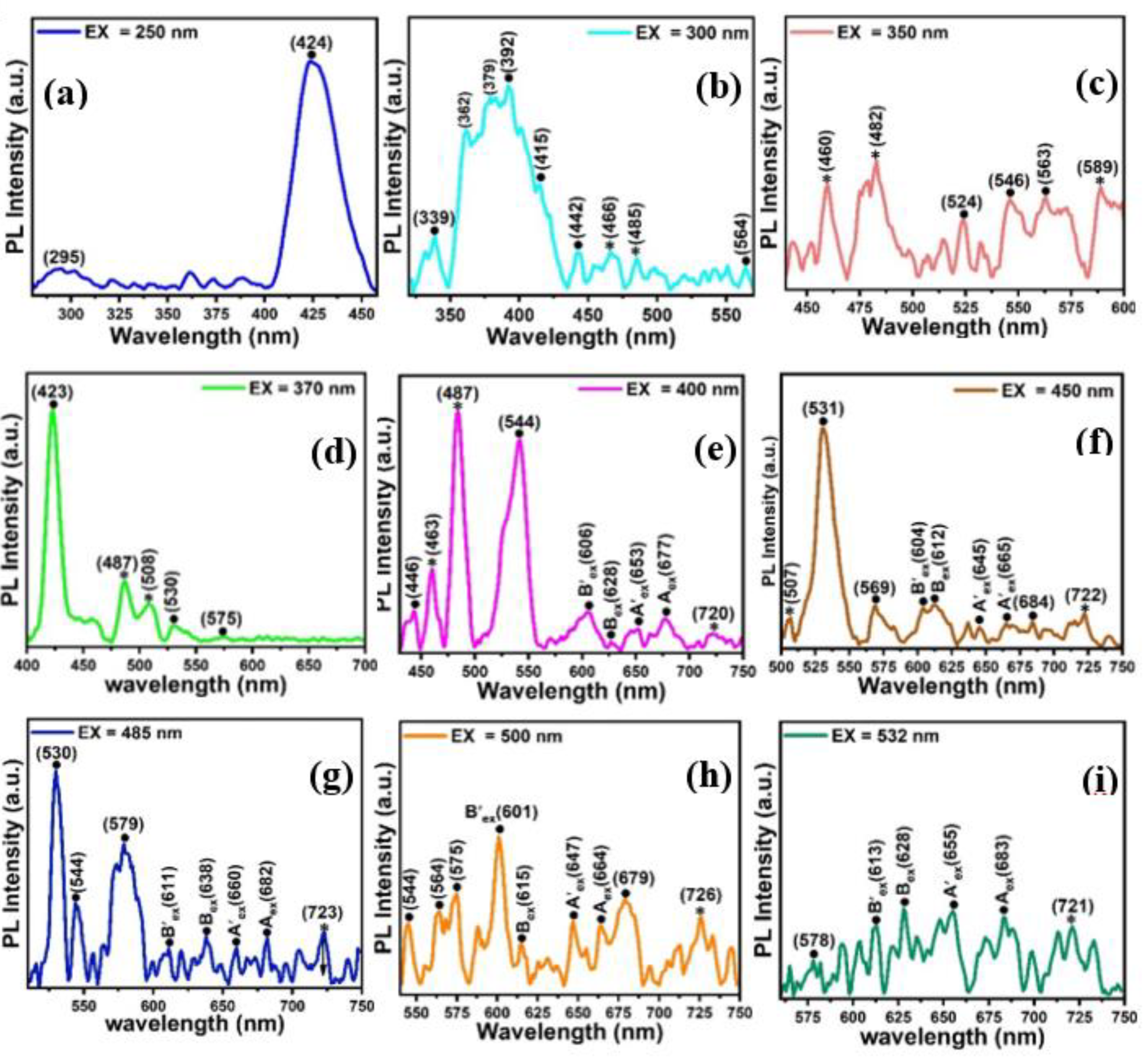
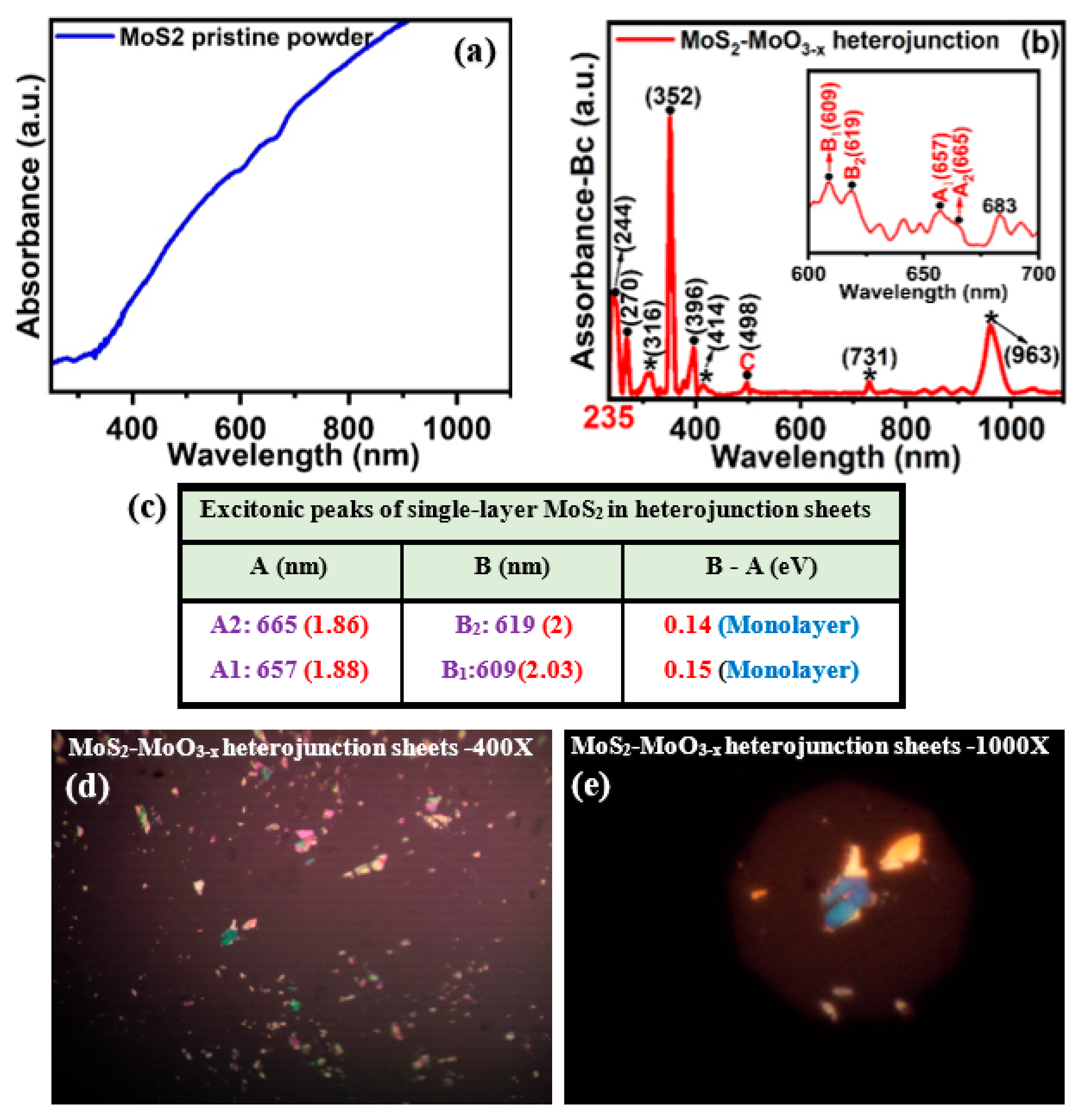
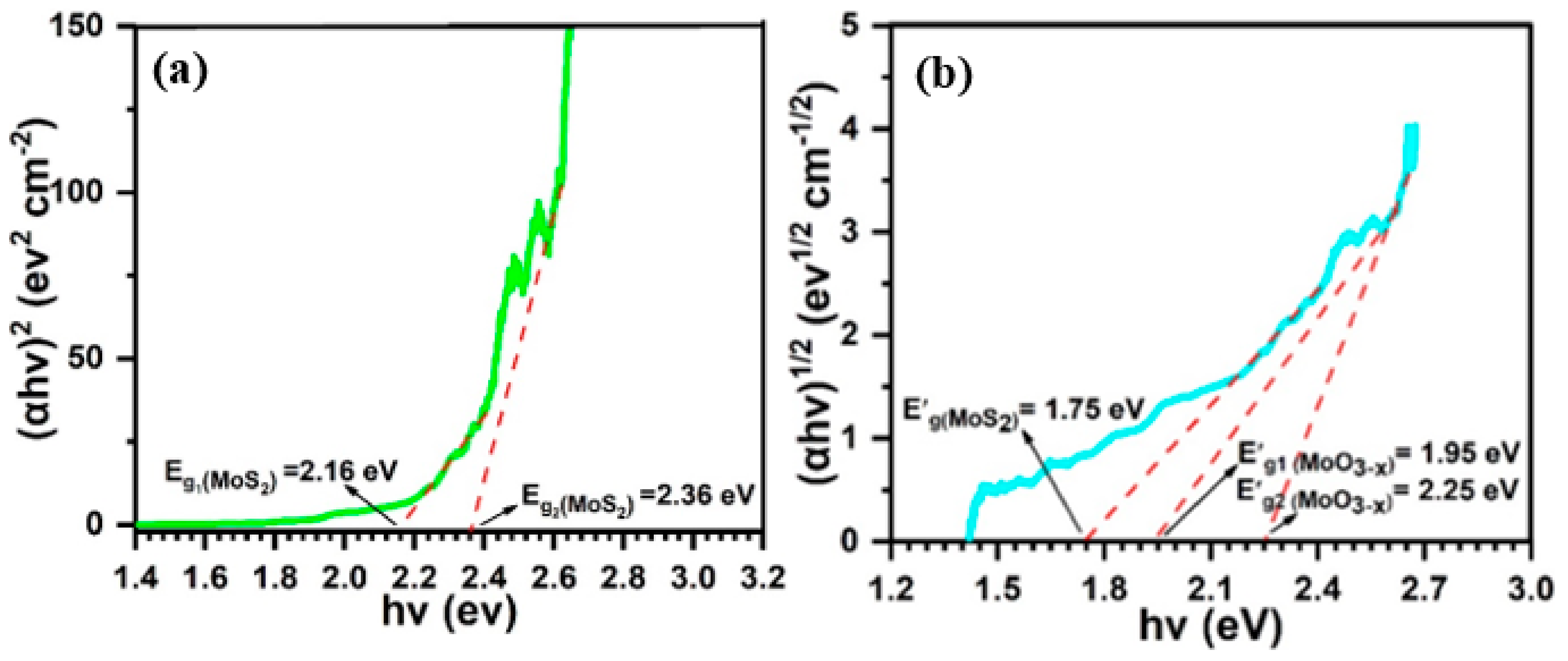
2.2. Optical Analysis

The optical absorption in the UV–visible and NIR regions is a characteristic related to the band structure of a semiconductor [55]. In order to study the optical properties of the MoS2-MoO3-x heterojunction sheets, the optical spectrum of the heterojunction sheets and the pristine MoS2 were studied, as shown in Figure 4. The peaks related to the MoS2 and MoO3-x phases were marked by (•) and (*) signs, respectively. No characteristic absorption peaks appeared in the pristine MoS2 spectrum (Figure 4a), because it has an indirect band gap [45,55]. The electronic, optical, and electrochemical properties of nano-scale semiconductors are size-dependent due to quantum confinement [56]. Concerning this, the absorption peaks located at 352 and 396 nm in Figure 4b can be assigned to the presence of MoS2 nanosheets with small sizes due to the quantum confinement effect [17,56,57]. Meanwhile, the absorption peaks observed at 244 and 270 nm of the UV region can be ascribed to the excitonic characteristics of MoS2 QDs [17,18,47].
It is worth noting that the single-layer 2H-MoS2 has the two low-energy absorption peaks of A and B between 600 and 700 nm as the excitonic peaks [17,58,59]. The valence band (VB) is split at the K-point of the Brillouin zone due to spin–orbit coupling (SOC), which results in the generation of two separate exciton bands (A and B excitonic bands) and the direct gap transitions [17,58,59,60]. In this work, MoS2-MoO3-x single layers with average lateral dimensions of ~70 nm possess the excitonic absorption peaks of A and B between 600 and 700 nm. There are two pairs of excitonic peaks of single-layer MoS2, i.e., (A1, B1) and (A2, B2) peaks (see the inset of Figure 4b), because of the existence of dispersity in the lateral size of single layers. The position and photon energy of excitonic peaks related to the single-layer MoS2 domains in single-layer heterojunctions are evaluated and presented in Figure 4c using the equation E g = h c λ (Eg, h, c, and λ are energy gap, Planck’s constant, light speed, and wavelength of absorption peak, respectively) [45]. The splitting energy difference of 0.14 and 0.15 eV between exciton peaks A and B (Figure 4c) confirmed the existence of MoS2 single layers in our sample, while it increased with increasing MoS2 film thickness, reaching 0.16 eV in the bilayer and 0.19 eV in the bulk [17,58]. The high-energy exciton peak C at 498 nm (2.48 eV) originates from inter-band transitions with high state density from the deep valence band to the conduction of MoS2 nanosheets [17,56,58,59]. The peak C at 2.48 eV can be associated with the optical absorption of 2H-MoS2 small-sized nanosheets due to the quantum effects [17,58].
In the absorption spectrum of the MoS2-MoO3-x heterojunction sheets, the optical absorption peak at 316 nm was attributed to the MoO3-x QDs [10,33,46,54,61]. The peaks located at 731 and 963 nm in the visible and NIR regions were related to the LSPR optical absorption of plasmonic MoO3-x domains [10,35,37,38,54] which are highly effective for photocatalytic activities [9,37]. In fact, the appearance of LSPR peaks confirmed the existence of oxygen-vacancy-rich MoO3-x domains with strong reducing capacity [35]. The presence of MoO3-x phase in the nanosheets is expected to replace or complement the noble metals in a wide range of photonic applications [37]. Figure 4d,e show optical microscopic images of the MoS2-MoO3-x heterojunction sheets with magnification of 400× and 1000×, respectively. The difference in color observed is due to the difference in the number of layers of nanosheets.
The absorption spectrum is sufficient to investigate the energy levels of MoS2-MoO3-x heterojunction. However, some specific signatures in PL emission spectra strongly confirm the presence of single layers and MoS2 phase domain in heterojunction [17,49,58]. Hence, PL spectroscopy was carried out for further examination of heterojunction. The PL spectra are also helpful to investigate optical properties such as the separation and recombination of electron–hole pairs as the primary processes in the field of photocatalysis [62]. The photoluminescence emission (PLE) spectra of heterojunction sheets were recorded at excitation wavelengths of 250, 300, 370, 400, 450, 485, 500, and 532 nm, at room temperature (Figure 5). The MoS2-MoO3-x heterojunction sheets showed the excitation-dependent luminescence emissions, because both MoS2 and MoO3-x nanosheets possess excitation-dependent PL emissions [17,36,46,47]. In Figure 5, the emission peaks related to the MoS2 and MoO3-x phases were marked with • and * signs, respectively. In the wavelength range between 600 and 700 nm, the PL peaks of Aex, Bex and A′ex, B′ex were attributed to excitations of single-layer MoS2 domains of MoS2-MoO3-x heterojunction nanosheets [47,49,58,60]. The peaks of Aex, A′ex and Bex,B′ex are associated with the direct gap transitions at KA KA′(K′B K′B′) points, the Brillouin zone, and the energy difference between the Aex and Bex peaks or A′ex and B′ex peaks, corresponding to the valence-band splitting due to the strong spin−orbital interaction [43,49]. The existence of the two pair PL emission peaks is due to the dispersion in lateral size of single-layer MoS2 domains of heterojunctions. The direct gap transitions of the Bex and B′ex peaks happen between the conduction band and a lower-lying valence band [43]. The weak intensity of excitation peaks of (Aex, Bex) and (A′ex, B′ex) indicates the low recombination of photoexcited charge carriers due to the effective separation of the photoexcited charge carriers [11]. The PLE peaks located at 684 nm (spectrum f) and 679 nm (spectrum of h) are attributed to the MoS2 bound excitons formed by localized excitons at defect sites [26], and these emission peaks can also be related to the direct band gap emissions [63]. Generally, the MoS2 nanosheets (depending on their size and the excitation wavelength) possess emission around 450–600 nm due to quantum confinement [17]. Hence, in this work, the obvious emission maxima located at 564, 563, 575, 579, 564, 575, 578 [64], 569 [17,64], 524, 546 [57], 530, 531, and 544 nm [17,57] can be attributed to surface recombination in quantum-confined MoS2 regions [64]. MoS2 QDs with excitation-dependent characteristic emission spectra emit a distinct blue PL under UV excitation wavelengths [47]. In spectra of Figure 5, the obvious emissions located at 424, 423 [18,47], 339 [48], 392 [18], 415 [47,57], 442, and 446 nm [65] excited by the wavelengths of 250, 300, 350, 370, and 400 nm were attributed to the MoS2 nanoscale regions.
The PL analysis for MoO3-x nanostructures is an important characteristic that offers extraordinary optical properties owing to the wide range of nonstoichiometric MoO3-x [36]. The optical band gap energies and PL emissions of MoO3-x nanostructures are also excitation-dependent [36,46] due to oxygen vacancies and defects [46]. The PLE peaks observed at 720, 722, 723, 726, and 721 nm (see the spectra of e–i of Figure 5) were ascribed to the MoO3-x nanoscale domains [66]. The PLE peaks that were excited with the different wavelengths located at 466, 460, 463 [36,46], 485, 482, 487 [46,61,67], 589 [46,66], 487 [46], 508, and 507 nm [46] correspond to the presence of MoO3-x QDs in the samples. The PLE peaks at 466, 460, and 463 nm can also be related to the band-to-band radiative recombination of photo-excited electrons and holes [36], and the PLE peaks at 485, 482, and 487 nm can be related to recombination between the conduction bands and the valence bands in MoO3-x [66]. As a basic feature, the generated hole–electron pairs in plasmonic MoO3-x nanomaterials under irradiation of LSPR excitation can activate chemical reactions (such as water splitting, methylene blue reduction) on their surface [35,37].
To estimate the optical band gap energy (Eg) of the MoS2-MoO3-x heterojunction sheets, the optical transmittance spectrum of the samples was recorded by DTS. Then, the Tauc plot was used to determine the band gap of the samples using Tauc’s relation [(αhν)1/n = C × (hν–Eg)], where hν is the incident photon energy, C is the proportionality constant, Eg is the band gap energy, and n = ½ and 2 for direct and indirect band gap, respectively [60,68,69]. In this regard, the curves of (αhν)2 and (αhν)1/2 versus photon energy (hν), derived from the transmittance spectra, were fitted to the Tauc model [34,60] (see Figure 6). The band gap energy of 2.16 and 2.36 eV (Figure 6a) can be ascribed to the direct band gap energies of single-layer MoS2 domains of the heterojunctions, and the value of 1.75 eV (Figure 6b) can be assigned to the indirect band gap energy of the part of MoS2 nanosheets of heterojunctions. The up-shift of MoS2 indirect band gap energy from 1.2 eV in pristine to 1.75 eV in nanosheets indicates effective exfoliation and induced quantum confinement [59,70]. Moreover, the values of 1.95 and 2.25 eV can be ascribed to the indirect band gap energies of MoO3-x domains (Figure 6b). The existence of two direct band gap energies is owing to the dispersion in lateral sizes of single-layer MoS2 domains of heterojunctions, and the existence of two indirect band gap energies related to MoO3-x domains is due to the presence of oxygen vacancies in MoO3-x. The narrower indirect band gap energy of MoO3-x domains of the heterojunction nanosheets (~1.95 and 2.25 eV) than that of MoO3 (~3 eV) is due to the existence of oxygen vacancies, which improve the carriers’ mobility and enhance photocatalytic activity [10,30,71]. The simultaneous presence of direct and indirect band gap energies in the MoS2-MoO3-x heterojunction sheets, especially the smaller indirect band gap energies as compared to the larger direct band gap ones, provides a more efficient photocatalyst under visible as well as solar light irradiation [69].

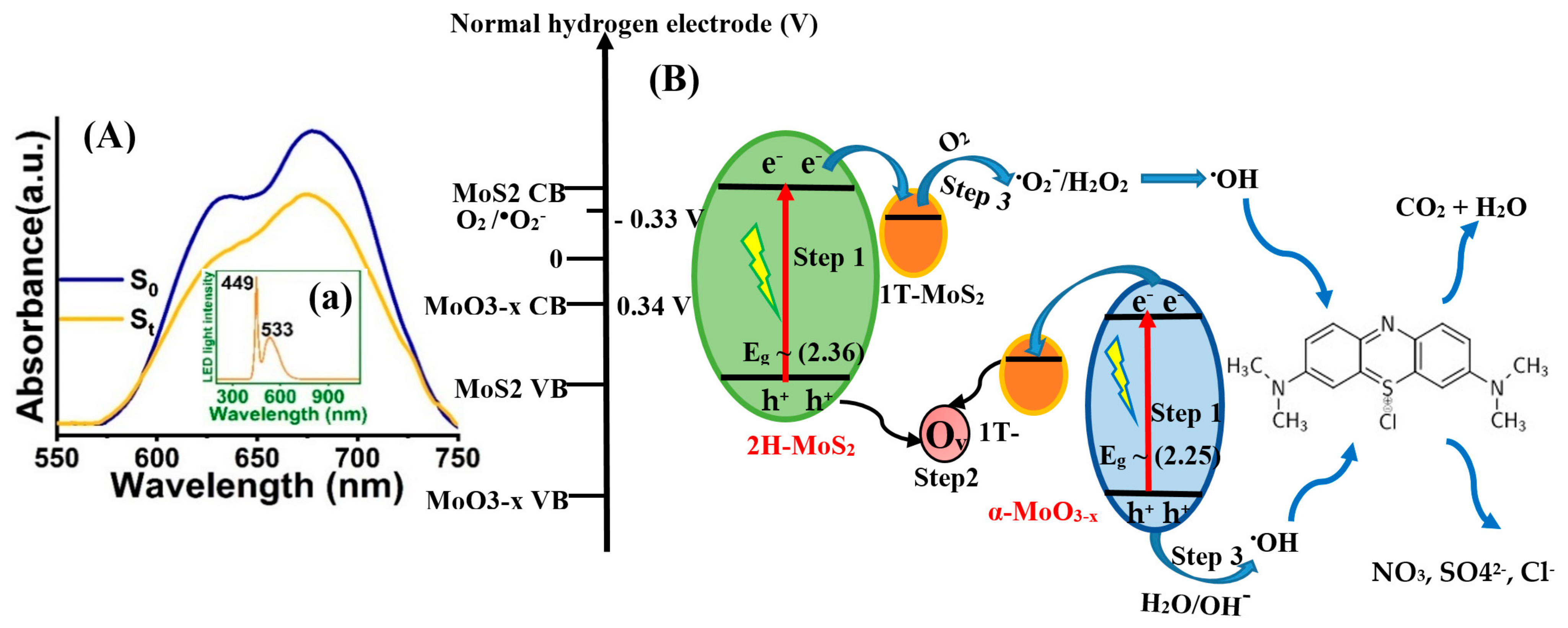
2.3. Photocatalytic Activity Test

The MoS2-MoO3-x heterojunction can be employed as a novel and efficient photocatalyst for harvesting the visible light due to superior adsorption capacity, tunable band structure of MoS2 and MoO3-x, and the effective separation of electron–hole pairs [4,11,35,37,54]. The simultaneous presence of considerable open metal edges, ultrathin nanosheets, 1T-MoS2 structural phase, sheet-like morphology, and high surface area in MoS2-MoO3-x heterojunctions result in extraordinary catalytic activity [22,23,72]. The MoO3-x domains also enhance the photocatalytic activity by broadening the light absorption range from 200 to 1000 nm, due to the oxygen vacancies facilitating the separation of photoexcited electron–hole pairs and preventing their fast recombination [11,30,41]. In this work, the photocatalytic performance of MoS2-MoO3-x heterojunction nanosheets was examined by photocatalytic degradation of methylene blue (MB) dye under visible light irradiation.
The emission spectrum of the LED lamp applied in the photocatalytic test (which is located at 449 nm (2.76 eV) and 553 nm (2.32 eV) visible light range) is shown in Figure 7A (in the inset). This source would be suitable for exciting the electron–hole pairs of MoS2-MoO3-x heterojunctions due to values of the direct and indirect band gap energies including 2.16, 2.36, 1.75, 1.95, and 2.25 eV determined by the DTS analysis (see, Figure 6). The characteristic absorption of MB at 665 nm [33] was chosen as the parameter to be monitored for the photocatalytic degradation process. The CB and VB edge positions of MoS2 and MoO3-x can be calculated by the DTS spectra and Mott–Schottky (MS) plots as reported by Huang et al. [11]. In this regard, the band gap energies of MoS2 and MoO3-x were calculated by DTS analysis (Figure 6), and then the approximate positions of their conduction band (CB) and valence band (VB) were estimated using References [11,20,21].
There are two approaches to describing the mechanism of the photocatalytic process: (1) Under light excitation, the excited electron can easily transfer from the MoS2 CB (conduction band) to the MoO3-x CB, and the holes in the MoO3-x VB (valance band) can easily transfer to the MoS2 VB [30]. However, according to the literature, the CB potential of MoO3-x (0.34 V) is more positive than that of O2/O2 (−0.33 V), and thus the superoxide anions (O2) could not be generated [11], while the O2 is the major active species in dye degradation. Therefore, another approach would be considered for the photocatalytic activity of the MoS2-MoO3-x heterojunction. (2) The excited electrons of MoS2 and MoO3-x can separately jump from their VB to CB, at step 1 (see Figure 7B). The 1T-MoS2 phase as a co-catalyst with special metal properties is a good electron acceptor, which can facilitate and accelerate the electron transfer to participate in the redox reaction and eventually enhances photocatalytic activity [29,39]. Hence, the excited-state electrons in the 2H-MoS2 and α-MoO3-x tend to transfer onto 1T-MoS2 [29]. Meanwhile, oxygen vacancies (Ov) in MoO3-x with broad light absorption range can serve as a recombination center to keep the charge balance [11]. Oxygen vacancies can receive the electrons from the 1T-MoS2 (electrons transferred from α-MoO3-x to 1T-MoS2) and holes from MoS2 VB (step 2) [11]. Thus, oxygen vacancies (Ov) of the MoO3-x cause the promotion of the separation efficiency of photoexcited charge carriers and eventually enhance photocatalytic activity of MoS2-MoO3-x heterojunction [11]. The effective separation of the electron–hole pairs may contribute to producing a high amount of active radicals from the harvested photons according to the following reactions in step 3 [29,30,62,66,69]:
[ MoS 2 - MoO 3 - x heterojunction ] photocatalyst + h ν [ MoS 2 - MoO 3 x heterojunction ] photocatalyst ( e + h + ) H 2 O H + + O H ; O H + h + O H H 2 O + h + H + + O H O 2 + e O 2 ; O 2 + 2 H + H 2 O 2 O 2 + 2 H + + 2 e H 2 O 2 H 2 O 2 + e O H + O H ; H + + O H H 2 O H 2 O 2 + H + + e O H + H 2 O H 2 O 2 / O H + M B C O 2 + H 2 O + (Degradation or oxidation of MB)
Upon light excitation, the generated electron–hole pairs are trapped on the surface of the photocatalyst, while water and hydroxyl groups are subsequently adsorbed on it. The generated electron–hole pairs initiate redox reactions; the holes in MoO3-x may react with absorbed water or hydroxide ions as hole scavengers (hole acceptor) to form strong oxidizing hydroxyl radicals (OH) [29,30,66]. In addition, the excited electrons in the 2H-MoS2, which can transfer into the 1T-MoS2 as a co-catalyst, can react with adsorbed oxygen, as electron scavengers (electron acceptor) can produce the oxidizing radicals (O2 and H2O2) and eventually the hydroxyl radicals (OH) [29,30]. Meanwhile, the oxidizing radicals of O2 and H2O2 prevent the recombination of the photoinduced e − h+ pairs and enhance quantum efficiency and photocatalytic activity [30,73]. During photocatalytic degradation, the generated active radical species such as OH and HO2 first break the N– CH3 bond, and then –CH3 is oxidized to form HCHO or HCOOH [74]. The free radicals (OH and HO2) then break the C–S and C–N bonds of thionine molecules to produce relatively unstable smaller organic byproducts. These oxidization reactions continue until the MB degrades completely to produce smaller inorganic molecules, such as H2O, Cl, CO2, SO42−, and NO3 [74].
Here, the main characteristics of MoS2-MoO3-x single-layer heterojunction are compared with the corresponding heterojunction samples in Table 1. The extraordinary photocatalytic activity of MoS2-MoO3-x heterojunction under visible light can be ascribed to following factors: (1) the existence of MoS2 single layers with a very high and fast absorption capacity in the visible light region due to direct band gap energy and larger value than the indirect band gap energies; (2) the presence of the ultrathin 1T- and 2H-MoS2 nanosheets with high electron mobility and catalytic activity; (3) the presence of MoO3-x domains as plasmonic photocatalyst with narrow band gap energy and broad light absorption range, which facilitate charge carrier generation, inhibit the undesirable electron–hole recombination, and promote the electron-hole separation; and (4) the synergistic effect of the 1T/2H-MoS2 and MoO3-x heterojunction sheets in the promotion of the separation of the photoelectron–hole pairs.

3. Conclusions

In summary, single-layer MoS2-MoO3-x heterojunction nanosheets (with lateral average dimensions of ~70 nm) were synthesized through a two-step combined method. The nanosheets showed an excitation-dependent PL behavior along with visible-light-induced photocatalytic activity. The existence of plasmonic MoO3-x domains with a broad light absorption due to the oxygen vacancies promoted the essential photocatalytic activity of single-layer MoS2 sheets by facilitating separation of photoexcited electron–hole pairs and preventing their fast recombination. Moreover, formation of the co-catalyst 1T-MoS2 phase with special metallic properties (such as working as an electron acceptor) resulted in facilitating and accelerating the electron transfer for participation in the redox reaction and eventually enhancing the photocatalytic activity. This research can drive further works on fabrication of 2D materials having domains with various chemical compositions in a single sheet, i.e., 2D heterojunctions. The unique characteristics of the synthesized MoS2-MoO3-x heterojunction nanosheets can result in promising applications in upcoming nanotechnology-based medicine, which highly requires biocompatible nanomaterials with simultaneous photoluminescence and photocatalytic features, such as tumor targeting, imaging, and phototherapy.

4. Experimental Section

4.1. Materials

Tetrahydrofuran (THF, C4H8O, anhydrous, ≥99.9%, inhibitor-free, Sigma Aldrich, St. Louis, MO, USA) as a solvent, bulk MoS2 powder (99%, Sigma Aldrich), sodium rods (Na, 22.99 g/mol, for synthesis (protective liquid: paraffin oil), Merck Millipore), naphthalene (128.17 g/mol, for synthesis, Merck Millipore), n-Hexane (CH3(CH2)4CH3, 86.18 g/mol, Analytical Reagents for General Use, Sigma Aldrich), acetone (CH3COCH3, 58.08 g/mol, Grade: Ph Eur, BP, JPE, NF, Merck Millipore), ethanol (C₂H₅OH, ≥99.9%, 46.07 g/mol, absolute for analysis, Merck Millipore), isopropyl alcohol (IPA, CH3CH(OH)CH3, 60.1 g/mol for analysis, Merck Millipore) were purchased in analytical reagent grade and applied as received. Ultrapure deionized distilled water with resistivity of 18.2 MΩ cm at 25 °C was used throughout the experiment.

4.2. Two-Step Preparation of MoS2-MoO3-x Single-Layer Heterojunctions

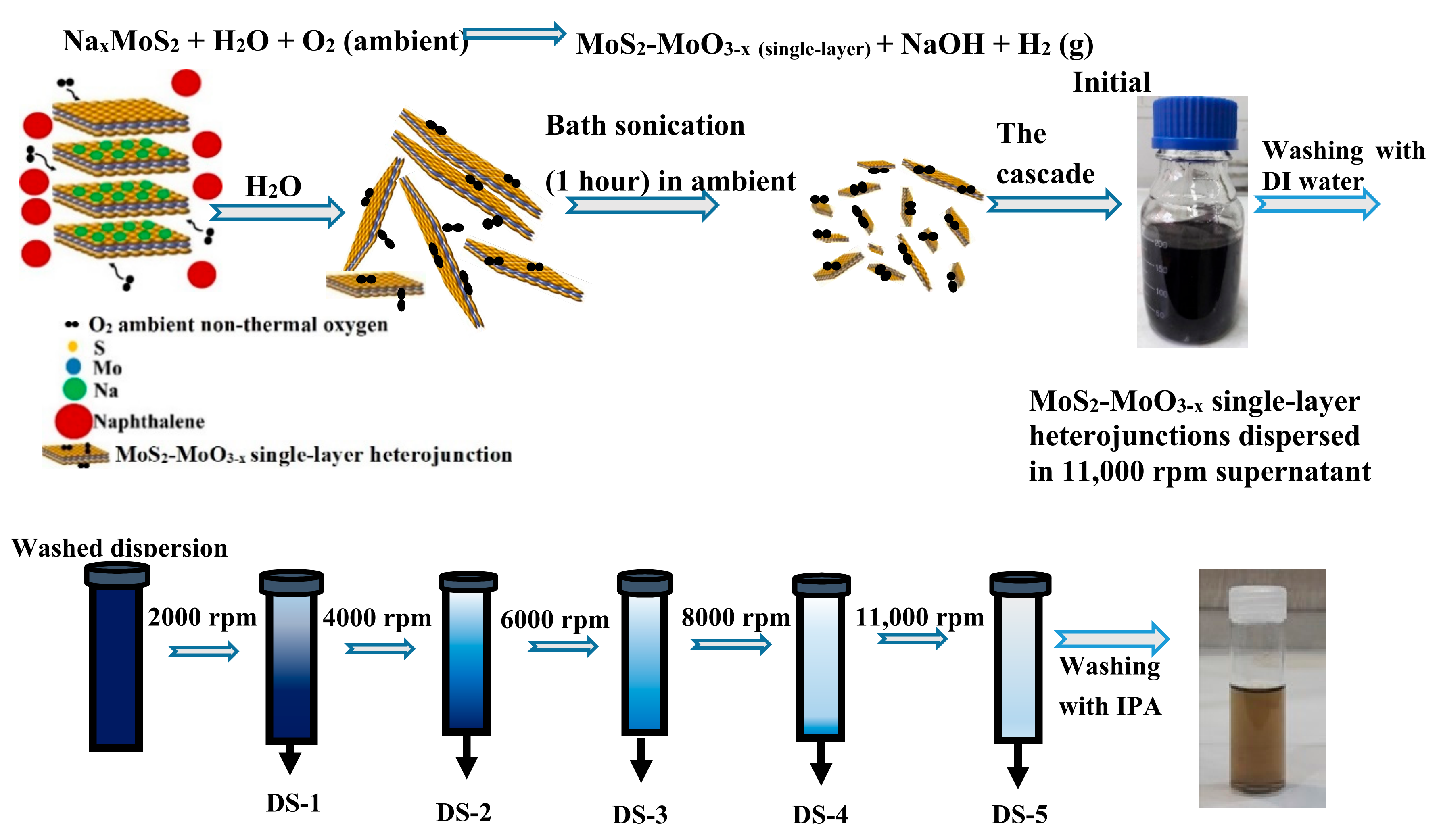
4.2.1. Exfoliation of Pristine MoS2 into Single Layers via Sodium Intercalation and Hydration

In the first step, 100 mL anhydrous tetrahydrofuran (THF) was poured into a 500 mL laboratory glass bottle followed by adding 8 g naphthalene. The mixture was continuously stirred using a magnetic bar (500 rpm) to allow mass transfer. Then, to prepare alkali naphthalenide solution, 1.4 g sodium metal was added to the mixture. In order to prevent sodium oxidation, sodium was stored in paraffin oil. It was washed with N-hexane before being used to remove paraffin oil, completely. In order to enhance the reaction kinetics and to prevent sodium oxidation, sodium metal was wired and added to the mixture at a very high speed. After complete dissolution of sodium by vigorous stirring for 2 h, a dark-blue mixture was obtained. Then, for intercalating sodium naphthalenide into the pristine MoS2, 2.0 g powder of pristine MoS2 was dispersed in the reaction mixture and stirred for 12 h.
The sodium-intercalated materials were exfoliated by slowly adding 200 mL DI water. By adding DI water, the self-exfoliation process, along with oxidation and hydration reactions, proceeded much more intensively into the interlayer space, resulting in effective exfoliation. In this step, the hydrogen gas as a byproduct was generated in the form of a large number of bubbles due to the reaction of water with the intercalated sodium between the MoS2 layers, which break and exfoliate the layered MoS2 as the driving force of spatial separation of the layers (as previously applied for graphene exfoliation [75]). The mixture is post-sonicated in a low-power ice-water sonic bath for 1 h [19], in order to complete the exfoliating and to form a homogeneous suspension through a sonochemical cavitation phenomena [17]. The resultant dark-blue dispersion with pH = 12 was produced and considered an initial dispersion (Figure 8).

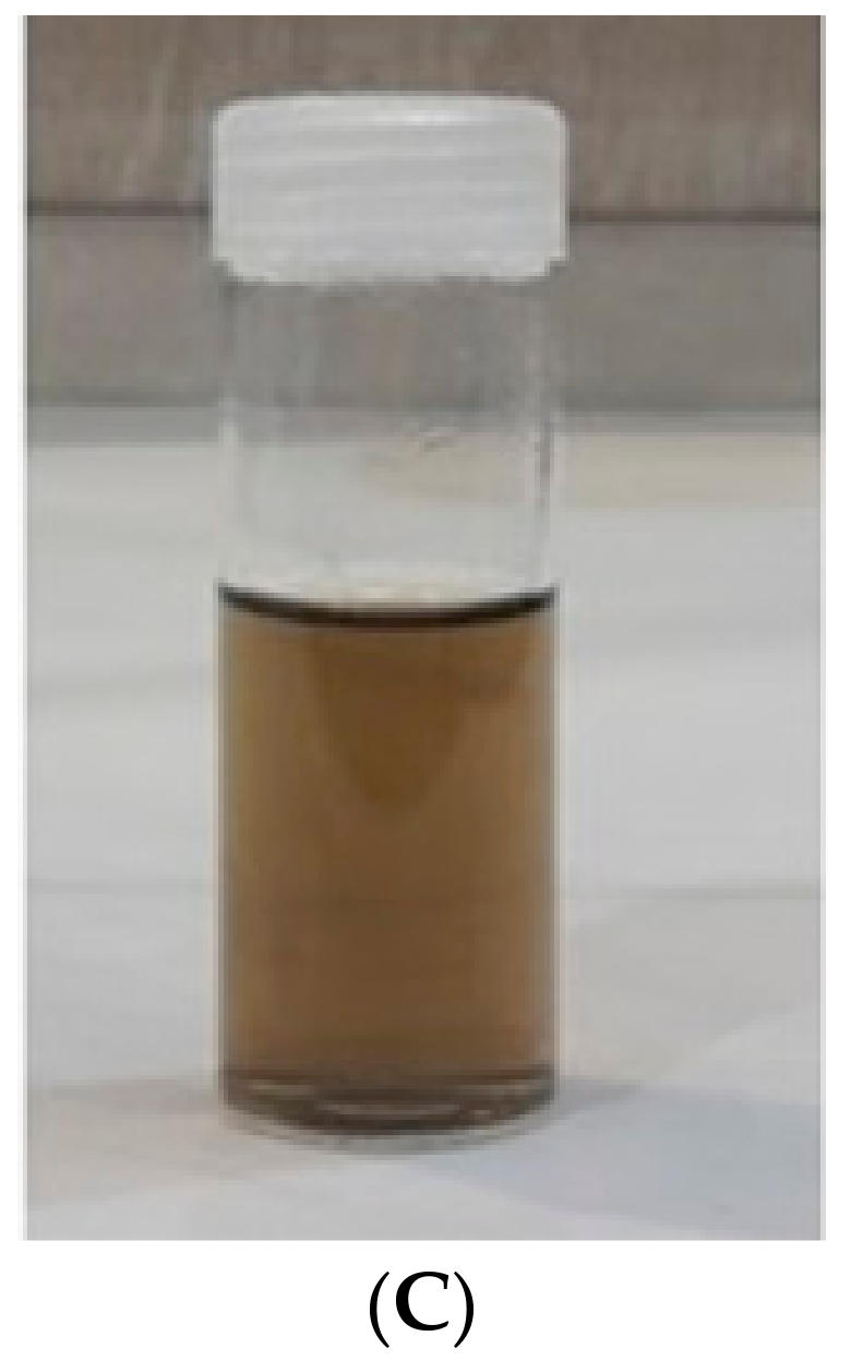
4.2.2. The Centrifugation Cascades for Extracting MoS2-MoO3-x Single-Layer Heterojunctions

The second step involves washing and extracting single-layer MoS2-MoO3-x heterojunction nanosheets from the initial dispersion. In order to remove THF as solvent, excess sodium, NaOH, and access to neutral solution pH, the initial dispersion was washed 4 times with DI water by centrifuging dispersion in 21,000 rpm (41,415 g). The resultant sediments were redispersed in DI water by mild sonication every time. The earlier centrifuges were performed at a very low temperature to prevent the ignition of tetrahydrofuran. After the fourth washing, the sediment was redispersed and the obtained dispersion was considered as the washed dispersion (Figure 8). The dispersed single-layer heterojunctions can be separated from initial dispersion using controlled centrifugation cascades (Table 2) by sequentially increasing rotation speeds [76]. This was performed by a short initial centrifugation at low rpm to eliminate thick and unexfoliated flakes in the sediment, and the obtained supernatant was centrifuged at a faster rpm in the next step. Thus, the resultant supernatant and sediment in each step of centrifugation included thinner and thick nanosheets, respectively. Finally, in the fifth centrifugation step, the 11,000 rpm supernatant (SN) included a large number of single-layer MoS2-MoO3-x heterojunction nanosheets. All centrifugations were performed at room temperature, and all grey-black sediments were discarded.
Finally, after consecutive centrifugation cascades, the obtained 11,000 rpm SN were washed with isopropyl alcohol (IPA) for removing organic material residues (ROMs) by centrifuging 11,000 rpm SN in 21,000 rpm for 10 min. The obtained sediment was redispersed in DI water again. A schematic of a two-step combined method for preparing MoS2-MoO3-x single-layer heterojunctions dispersed into 11,000 rpm SN is presented in Figure 8.

4.2.3. The Application of MoS2-MoO3-x Heterojunctions for MB Photocatalytic Degradation

In a typical degradation experiment, 5 mL methylene blue solution with a concentration of 10 − 5 mM and 10 mL of 11,000 rpm SN with a concentration of 0.14 mg/mL were added into a 30 mL Pyrex beaker, and then they were magnetically and continuously stirred in the dark for a few minutes to ensure establishment of an adsorption–desorption equilibrium on the surface of the photocatalyst. The equilibrium concentration of MB in contact with the dispersed photocatalytic heterojunctions was considered as the initial MB concentration before the start of irradiation, which is referred to as solution before irradiation (S0). The Pyrex beaker containing solution of MB and photocatalyst was placed from 4 directions under 8 LED light irradiation of 1 W at a distance of approximately 10 cm from LED lamps (2 LEDs on each side). The solution after irradiation of a few hours was considered as the solution after irradiation (St).

4.3. Material Characterizations

The surface morphology of the samples was investigated by field-emission-scanning electron microscope (FESEM) using a MIRA3TESCAN-XMU (TESCAN, Brno, Czech Republic). The transmission electron microscopy (TEM) image of the nanosheets was accessed by using a Philips CM300 (Philips, Eindhoven, The Netherlands) operated at 200 kV. Atomic force microscopy (AFM) was performed using a ThermoMicroscopes Autoprobe CP Research (Veeco instruments, Sunnyvale, CA, USA) in a contact mode. The lateral size distributions and height profile of the sheets were determined by analyzing the AFM images by using Image Processing and Data analysis ver.2.1.15 (Veeco) software. X-ray diffraction (XRD) data were acquired by a Philips X’Pert PANalytical X-ray diffractometer (Malvern Panalytical, Netherlands) using Cu Kα radiation source with wavelength of 1.5406 Å and a step size of Δ2θ = 0.03° at room temperature. Raman spectroscopy was performed with a non-resonant excitation using a 532 nm Nd:YAG laser (Tekscan, Tekram P50C0R10, Iran). The optical properties of the samples were evaluated by UV–visible–NIR absorption measurements, photoluminescence (PL) spectroscopy, and diffuse transmittance spectroscopy (DTS). UV–visible absorption measurements were performed by using a UV-Vis spectrophotometer (Lambda 25, PerkinElmer, Waltham, MA, USA). Photoluminescence (PL) emissions were recorded by using a Cary Eclipse Fluorescence Spectrophotometer (Agilent Technologies, Santa Clara, CA, USA). DTS measurements were carried out by using an Avaspec 2048 TEC (Avantes, Netherlands) with AvaLamp DH-S Setup. The ultrasonic bath was performed by a sonicator (Elmasonic P60H, Elma Schmidbauer GmbH, Singen Germany). All centrifugations were carried out by using a centrifuge apparatus with 3-30KS model (Sigma Laborzentrifuge GmbH D-37520, Osterode- am- Harz, Germany).
For obtaining FESEM images, a small amount of 11,000 rpm supernatant (SN) was freeze-dried. The TEM sample preparation was performed by depositing a few drops of the dispersion of the 11,000 rpm SN onto TEM grids. In order to prepare the samples for AFM, a small amount of 11,000 rpm SN was diluted with DI water and then drop-casted on recently cleaned SiO2/Si surface. The aggregation can occur during the deposition. It is important to ensure that thickness statistics of single layers are not strongly influenced by aggregation effects on the substrate in AFM analysis. Raman spectroscopy of heterojunctions was obtained through depositing 11,000 rpm SN on a cleaned SiO2/Si wafer.

Author Contributions

Conceptualization, M.S. and O.A.; methodology, M.S. and O.A.; software, M.S. and O.A.; validation, M.S. and O.A.; formal analysis, M.S. and O.A.; investigation, M.S. and O.A.; resources, O.A. and H.F.; data curation, M.S. and O.A.; writing—original draft preparation, M.S. and O.A.; writing—review and editing, M.S. and O.A.; visualization, M.S. and O.A.; supervision, O.A. and H.F.; project administration, O.A. and H.F.; funding acquisition, O.A. and H.F. All authors have read and agreed to the published version of the manuscript.

Funding

This research received no external funding.

Data Availability Statement

The data presented in this study are available on request from the corresponding author. The data are not publicly available due to privacy restrictions.

Conflicts of Interest

The authors declare no conflict of interest.

References

  1. Christopher, P.; Xin, H.; Marimuthu, A.; Linic, S. Singular characteristics and unique chemical bond activation mechanisms of photocatalytic reactions on plasmonic nanostructures. Nat. Mater. 2012, 11, 1044–1050. [Google Scholar] [CrossRef] [PubMed]
  2. Albu, S.P.; Ghicov, A.; Macak, J.M.; Hahn, R.; Schmuki, P. Self-organized, free-standing TiO2 nanotube membrane for flow-through photocatalytic applications. Nano Lett. 2007, 7, 1286–1289. [Google Scholar] [CrossRef] [PubMed]
  3. Akhavan, O.; Ghaderi, E. Flash photo stimulation of human neural stem cells on graphene/TiO2 heterojunction for differentiation into neurons. Nanoscale 2013, 5, 10316–10326. [Google Scholar] [CrossRef] [PubMed]
  4. Wu, M.-H.; Li, L.; Liu, N.; Wang, D.-J.; Xue, Y.-C.; Tang, L. Molybdenum disulfide (MoS2) as a co-catalyst for photocatalytic degradation of organic contaminants: A review. Process Saf. Environ. Prot. 2018, 118, 40–58. [Google Scholar] [CrossRef]
  5. Li, Z.; Meng, X.; Zhang, Z. Recent development on MoS2-based photocatalysis: A review. J. Photochem. Photobiol. C Photochem. Rev. 2018, 35, 39–55. [Google Scholar] [CrossRef]
  6. Akhavan, O.; Ghaderi, E. Cu and CuO nanoparticles immobilized by silica thin films as antibacterial materials and photocatalysts. Surf. Coatings Technol. 2010, 205, 219–223. [Google Scholar] [CrossRef]
  7. Akhavan, O.; Choobtashani, M.; Ghaderi, E. Protein degradation and RNA efflux of viruses photocatalyzed by graphene-tungsten oxide composite under visible light irradiation. J. Phys. Chem. C 2012, 116, 9653–9659. [Google Scholar] [CrossRef]
  8. Akhavan, O.; Ghaderi, E.; Rahimi, K. Adverse effects of graphene incorporated in TiO2 photocatalyst on minuscule animals under solar light irradiation. J. Mater. Chem. 2012, 22, 23260–23266. [Google Scholar] [CrossRef]
  9. Liu, Q.; Wu, Y.; Zhang, J.; Chen, K.; Huang, C.; Chen, H.; Qiu, X. Plasmonic MoO3-x nanosheets with tunable oxygen vacancies as efficient visible light responsive photocatalyst. Appl. Surf. Sci. 2019, 490, 395–402. [Google Scholar] [CrossRef]
  10. Etman, A.S.; Abdelhamid, H.N.; Yuan, Y.; Wang, L.; Zou, X.; Sun, J. Facile water-based strategy for synthesizing MoO3–x nanosheets: Efficient visible light photocatalysts for dye degradation. ACS Omega 2018, 3, 2193–2201. [Google Scholar] [CrossRef] [PubMed] [Green Version]
  11. Huang, L.; Zhang, F.; Li, Y.; Wang, H.; Wang, Q.; Wang, C.; Xu, H.; Li, H. Chemical reduction implanted oxygen vacancy on the surface of 1D MoO3-x/g-C3N4 composite for boosted LED light-driven photoactivity. J. Mater. Sci. 2019, 54, 5343–5358. [Google Scholar] [CrossRef]
  12. Akhavan, O.; Ghaderi, E.; Shirazian, S.A. Near infrared laser stimulation of human neural stem cells into neurons on graphene nanomesh semiconductors. Colloids Surf. B Biointerfaces 2015, 126, 313–321. [Google Scholar] [CrossRef] [PubMed]
  13. Akhavan, O. Graphene nanomesh by ZnO nanorod photocatalysts. ACS Nano 2010, 4, 4174–4180. [Google Scholar] [CrossRef] [PubMed]
  14. Akhavan, O. Lasting antibacterial activities of Ag-TiO2/Ag/a-TiO2 nanocomposite thin film photocatalysts under solar light irradiation. J. Colloid Interface Sci. 2009, 336, 117–124. [Google Scholar] [CrossRef] [PubMed]
  15. Akhavan, O.; Ghaderi, E. Photocatalytic reduction of graphene oxide nanosheets on TiO2 thin film for photoinactivation of bacteria in solar light irradiation. J. Phys. Chem. C 2009, 113, 20214–20220. [Google Scholar] [CrossRef]
  16. Sim, D.M.; Han, H.J.; Yim, S.; Choi, M.-J.; Jeon, J.; Jung, Y.S. Long-term stable 2H-MoS2 dispersion: Critical role of solvent for simultaneous phase restoration and surface functionalization of liquid-exfoliated MoS2. ACS Omega 2017, 2, 4678–4687. [Google Scholar] [CrossRef] [PubMed]
  17. Portone, A.; Romano, L.; Fasano, V.; Di Corato, R.; Camposeo, A.; Fabbri, F.; Cardarelli, F.; Pisignano, D.; Persano, L. Low-defectiveness exfoliation of MoS2 nanoparticles and their embedment in hybrid light-emitting polymer nanofibers. Nanoscale 2018, 10, 21748–21754. [Google Scholar] [CrossRef] [Green Version]
  18. Li, Y.; Wang, X.; Liu, M.; Luo, H.; Deng, L.; Huang, L.; Wei, S.; Zhou, C.; Xu, Y. Molybdenum disulfide quantum dots prepared by bipolar-electrode electrochemical scissoring. Nanomaterials 2019, 9, 906. [Google Scholar] [CrossRef] [PubMed] [Green Version]
  19. Zheng, J.; Zhang, H.; Dong, S.; Liu, Y.; Nai, C.T.; Shin, H.S.; Jeong, H.Y.; Liu, B.; Loh, K.P. High yield exfoliation of two-dimensional chalcogenides using sodium naphthalenide. Nat. Commun. 2014, 5, 2995. [Google Scholar] [CrossRef]
  20. Chen, J.; Liao, Y.; Wan, X.; Tie, S.; Zhang, B.; Lan, S.; Gao, X. A high performance MoO3@MoS2 porous nanorods for adsorption and photodegradation of dye. J. Solid State Chem. 2020, 291, 121652. [Google Scholar] [CrossRef]
  21. Lu, X.; Jin, Y.; Zhang, X.; Xu, G.; Wang, D.; Lv, J.; Zheng, Z.; Wu, Y. Controllable synthesis of graphitic C3N4/ultrathin MoS2 nanosheet hybrid nanostructures with enhanced photocatalytic performance. Dalt. Trans. 2016, 45, 15406–15414. [Google Scholar] [CrossRef] [PubMed]
  22. Li, G.; Zhang, D.; Qiao, Q.; Yu, Y.; Peterson, D.; Zafar, A.; Kumar, R.; Curtarolo, S.; Hunte, F.; Shannon, S.; et al. All the catalytic active sites of MoS2 for hydrogen evolution. J. Am. Chem. Soc. 2016, 138, 16632–16638. [Google Scholar] [CrossRef] [PubMed]
  23. Shi, S.; Sun, Z.; Hu, Y.H. Synthesis, stabilization and applications of 2-dimensional 1T metallic MoS2. J. Mater. Chem. A 2018, 6, 23932–23977. [Google Scholar] [CrossRef]
  24. Zak, A.; Feldman, Y.; Lyakhovitskaya, V.; Leitus, G.; Popovitz-Biro, R.; Wachtel, E.; Cohen, H.; Reich, S.; Tenne, R. Alkali metal intercalated fullerene-like MS2 (M = W, Mo) nanoparticles and their propertie. J. Am. Chem. Soc. 2002, 124, 4747–4758. [Google Scholar] [CrossRef]
  25. Wang, H.; Sofer, Z.; Moo, J.G.S.; Pumera, M. Simultaneous self-exfoliation and autonomous motion of MoS2 particles in water. Chem. Commun. 2015, 51, 9899–9902. [Google Scholar] [CrossRef] [Green Version]
  26. Voiry, D.; Mohite, A.; Chhowalla, M. Phase engineering of transition metal dichalcogenides. Chem. Soc. Rev. 2015, 44, 2702–2712. [Google Scholar] [CrossRef] [PubMed]
  27. Attanayake, N.H.; Thenuwara, A.C.; Patra, A.; Aulin, Y.V.; Tran, T.M.; Chakraborty, H.; Borguet, E.; Klein, M.L.; Perdew, J.P.; Strongin, D.R. Effect of intercalated metals on the electrocatalytic activity of 1T-MoS2 for the hydrogen evolution reaction. ACS Energy Lett. 2018, 3, 7–13. [Google Scholar] [CrossRef]
  28. Saber, M.R.; Khabiri, G.; Maarouf, A.A.; Ulbricht, M.; Khalil, A.S.G. A comparative study on the photocatalytic degradation of organic dyes using hybridized 1T/2H, 1T/3R and 2H MoS2 nano-sheets. RSC Adv. 2018, 8, 26364–26370. [Google Scholar] [CrossRef] [Green Version]
  29. Fan, H.; Wu, R.; Liu, H.; Yang, X.; Sun, Y.; Chen, C. Synthesis of metal-phase-assisted 1T@2H-MoS2 nanosheet-coated black TiO2 spheres with visible light photocatalytic activities. J. Mater. Sci. 2018, 53, 10302–10312. [Google Scholar] [CrossRef]
  30. Li, H.; Yu, K.; Tang, Z.; Fu, H.; Zhu, Z. High photocatalytic performance of a type-II α-MoO3@MoS2 heterojunction: From theory to experiment. Phys. Chem. Chem. Phys. 2016, 18, 14074–14085. [Google Scholar] [CrossRef] [PubMed]
  31. Zhu, Y.; Yao, Y.; Luo, Z.; Pan, C.; Yang, J.; Fang, Y.; Deng, H.; Liu, C.; Tan, Q.; Liu, F.; et al. Nanostructured MoO3 for Efficient Energy and Environmental Catalysis. Molecules 2020, 25, 18. [Google Scholar] [CrossRef] [PubMed] [Green Version]
  32. Baltrusaitis, J.; Mendoza-Sanchez, B.; Fernandez, V.; Veenstra, R.; Dukstiene, N.; Roberts, A.; Fairley, N. Generalized molybdenum oxide surface chemical state XPS determination via informed amorphous sample model. Appl. Surf. Sci. 2015, 326, 151–161. [Google Scholar] [CrossRef]
  33. Sreedhara, M.B.; Matte, H.S.S.R.; Govindaraj, A.; Rao, C.N.R. Synthesis, characterization, and properties of few-layer MoO3. Chem. An. Asian J. 2013, 8, 2430–2435. [Google Scholar] [CrossRef]
  34. Balendhran, S.; Walia, S.; Nili, H.; Ou, J.Z.; Zhuiykov, S.; Kaner, R.B.; Sriram, S.; Bhaskaran, M.; Kalantar-zadeh, K. Two-dimensional molybdenum trioxide and dichalcogenides. Adv. Funct. Mater. 2013, 23, 3952–3970. [Google Scholar] [CrossRef]
  35. Du, J.; Wang, J.; Deng, Y.; He, Y. Plasmonic hot electron transfer-induced multicolor MoO3-x-based chromogenic system for visual and colorimetric determination of silver(I). Microchim. Acta 2020, 187, 120. [Google Scholar] [CrossRef] [PubMed]
  36. Lu, X.; Wang, R.; Yang, F.; Jiao, W.; Liu, W.; Hao, L.; He, X. Preparation of MoO3 QDs through combining intercalation and thermal exfoliation. J. Mater. Chem. C 2016, 4, 6720–6726. [Google Scholar] [CrossRef]
  37. Tan, X.; Wang, L.; Cheng, C.; Yan, X.; Shen, B.; Zhang, J. Plasmonic MoO3-x@MoO3 nanosheets for highly sensitive SERS detection through nanoshell-isolated electromagnetic enhancement. Chem. Commun. 2016, 52, 2893–2896. [Google Scholar] [CrossRef] [PubMed]
  38. Bai, H.; Yi, W.; Li, J.; Xi, G.; Li, Y.; Yang, H.; Liu, J. Direct growth of defect-rich MoO3-x ultrathin nanobelts for efficiently catalyzed conversion of isopropyl alcohol to propylene under visible light. J. Mater. Chem. A 2016, 4, 1566–1571. [Google Scholar] [CrossRef]
  39. Patra, K.K.; Ghosalya, M.K.; Bajpai, H.; Raj, S.; Gopinath, C.S. Oxidative Disproportionation of MoS2/GO to MoS2/MoO3- x/RGO: Integrated and Plasmonic 2D-Multifunctional Nanocomposites for Solar Hydrogen Generation from Near-Infrared and Visible Regions. J. Phys. Chem. C 2019, 123, 21685–21693. [Google Scholar] [CrossRef]
  40. Datta, R.S.; Haque, F.; Mohiuddin, M.; Carey, B.J.; Syed, N.; Zavabeti, A.; Zhang, B.; Khan, H.; Berean, K.J.; Ou, J.Z.; et al. Highly active two dimensional α-MoO3-X for the electrocatalytic hydrogen evolution reaction. J. Mater. Chem. A 2017, 5, 24223–24231. [Google Scholar] [CrossRef]
  41. Zhao, H.Q.; Mao, X.; Zhou, D.; Feng, S.; Shi, X.; Ma, Y.; Wei, X.; Mao, Y. Bandgap modulation of MoS2 monolayer by thermal annealing and quick cooling. Nanoscale 2016, 8, 18995–19003. [Google Scholar] [CrossRef] [PubMed]
  42. Benson, J.; Li, M.; Wang, S.; Wang, P.; Papakonstantinou, P. Electrocatalytic Hydrogen evolution reaction on edges of a few layer molybdenum disulfide nanodots. ACS Appl. Mater. Interfaces 2015, 7, 14113–14122. [Google Scholar] [CrossRef] [Green Version]
  43. Sharma, L.; Botari, T.; Tiwary, C.S.; Halder, A. Hydrogen evolution at the in situ MoO3 /MoS2 heterojunctions created by nonthermal O2 plasma treatment. ACS Appl. Energy Mater. 2020, 3, 5333–5342. [Google Scholar] [CrossRef]
  44. Wang, D.; Zhang, X.; Bao, S.; Zhang, Z.; Fei, H.; Wu, Z. Phase engineering of a multiphasic 1T/2H MoS2 catalyst for highly efficient hydrogen evolution. J. Mater. Chem. A 2017, 5, 2681–2688. [Google Scholar] [CrossRef]
  45. Kim, C.; Nguyen, T.P.; Van Le, Q.; Jeon, J.M.; Jang, H.W.; Kim, S.Y. Performances of liquid-exfoliated transition metal dichalcogenides as hole injection layers in organic light-emitting diodes. Adv. Funct. Mater. 2015, 25, 4512–4519. [Google Scholar] [CrossRef]
  46. Chandoul, F.; Boukhachem, A.; Hosni, F.; Moussa, H.; Fayache, M.S.; Amlouk, M.; Schneider, R. Change of the properties of nanostructured MoO3 thin films using gamma-ray irradiation. Ceram. Int. 2018, 44, 12483–12490. [Google Scholar] [CrossRef]
  47. Qiao, W.; Yan, S.; Song, X.; Zhang, X.; He, X.; Zhong, W.; Du, Y. Luminescent monolayer MoS2 quantum dots produced by multi-exfoliation based on lithium intercalation. Appl. Surf. Sci. 2015, 359, 130–136. [Google Scholar] [CrossRef]
  48. Li, B.; Jiang, L.; Li, X.; Ran, P.; Zuo, P.; Wang, A.; Qu, L.; Zhao, Y.; Cheng, Z.; Lu, Y. Preparation of monolayer MoS2 quantum dots using temporally shaped femtosecond laser ablation of bulk MoS2 targets in water. Sci. Rep. 2017, 7, 11182. [Google Scholar] [CrossRef] [PubMed]
  49. Mouri, S.; Miyauchi, Y.; Matsuda, K. Tunable photoluminescence of monolayer MoS2 via chemical doping. Nano Lett. 2013, 13, 5944–5948. [Google Scholar] [CrossRef] [Green Version]
  50. Lee, C.; Yan, H.; Brus, L.E.; Heinz, T.F.; Hone, J.; Ryu, S. Anomalous lattice vibrations of single and few-layer MoS2. ACS Nano 2010, 4, 6–7. [Google Scholar] [CrossRef] [Green Version]
  51. Li, H.; Zhang, Q.; Yap, C.C.R.; Tay, B.K.; Edwin, T.H.T.; Olivier, A.; Baillargeat, D. From bulk to monolayer MoS2: Evolution of Raman scattering. Adv. Funct. Mater. 2012, 22, 1385–1390. [Google Scholar] [CrossRef]
  52. Deokar, G.; Rajput, N.S.; Vancsó, P.; Ravaux, F.; Jouiad, M.; Vignaud, D.; Cecchet, F.; Colomer, J.F. Large area growth of vertically aligned luminescent MoS2 nanosheets. Nanoscale 2017, 9, 277–287. [Google Scholar] [CrossRef] [PubMed]
  53. Seguin, L.; Figlarz, M.; Cavagnat, R.; Lassègues, J.-C.C. Infrared and Raman spectra of MoO3 molybdenum trioxides and MoO3 · xH2O molybdenum trioxide hydrates. Spectrochim. Acta Part A Mol. Biomol. Spectrosc. 1995, 51, 1323–1344. [Google Scholar] [CrossRef]
  54. Dieterle, M.; Weinberg, G.; Mestl, G. Raman spectroscopy of molybdenum oxides-Part I. Structural characterization of oxygen defects in MoO3-x by DR UV/VIS, Raman spectroscopy and X-ray diffraction. Phys. Chem. Chem. Phys. 2002, 4, 812–821. [Google Scholar] [CrossRef]
  55. Li, B.L.; Chen, L.X.; Zou, H.L.; Lei, J.L.; Luo, H.Q.; Li, N.B. Electrochemically induced Fenton reaction of nanoporous morphology. Nanoscale 2014, 6, 9831–9838. [Google Scholar] [CrossRef] [PubMed]
  56. Chikan, V.; Kelley, D.F. Size-dependent spectroscopy of MoS2 nanoclusters. J. Phys. Chem. B 2002, 106, 3794–3804. [Google Scholar] [CrossRef]
  57. Zhou, K.; Zhang, Y.; Xia, Z.; Wei, W. As-prepared MoS2 quantum dot as a facile fluorescent probe for long-term tracing of live cells. Nanotechnology 2016, 27, 275101. [Google Scholar] [CrossRef]
  58. Dhakal, K.P.; Duong, D.L.; Lee, J.; Nam, H.; Kim, M.; Kan, M.; Lee, Y.H.; Kim, J. Confocal absorption spectral imaging of MoS2: Optical transitions depending on the atomic thickness of intrinsic and chemically doped MoS2. Nanoscale 2014, 6, 13028–13035. [Google Scholar] [CrossRef] [Green Version]
  59. Mishra, A.K.; Lakshmi, K.V.; Huang, L. Eco-friendly synthesis of metal dichalcogenides nanosheets and their environmental remediation potential driven by visible light. Sci. Rep. 2015, 5, 15718. [Google Scholar] [CrossRef] [Green Version]
  60. Fadil, D.; Hossain, R.F.; Saenz, G.A.; Kaul, A.B. On the chemically-assisted excitonic enhancement in environmentally-friendly solution dispersions of two-dimensional MoS2 and WS2. J. Mater. Chem. C 2017, 5, 5323–5333. [Google Scholar] [CrossRef]
  61. Liu, X.; Zhang, W.; Yang, C.; Yao, Y.; Huang, L.; Li, S.; Wang, J.; Ji, Y. Rapid and selective fluorometric determination of tannic acid using MoO3-x quantum dots. Microchim. Acta 2019, 186, 247. [Google Scholar] [CrossRef]
  62. Singh, R.; Dutta, S. Synthesis and characterization of solar photoactive TiO2 nanoparticles with enhanced structural and optical properties. Adv. Powder Technol. 2018, 29, 211–219. [Google Scholar] [CrossRef]
  63. Nan, H.; Wang, Z.; Wang, W.; Liang, Z.; Lu, Y.; Chen, Q.; He, D.; Tan, P.; Miao, F.; Wang, X.; et al. Strong photoluminescence enhancement of MoS2 through defect engineering and oxygen bonding. ACS Nano 2014, 8, 5738–5745. [Google Scholar] [CrossRef] [Green Version]
  64. Gopalakrishnan, D.; Damien, D.; Shaijumon, M.M. MoS2 Quantum Dot-Interspersed Exfoliated MoS2. ACS Nano 2014, 8, 5297–5303. [Google Scholar] [CrossRef]
  65. Wu, J.-Y.Y.; Lin, M.-N.N.; De Wang, L.-D.; Zhang, T. Photoluminescence of MoS2 prepared by effective grinding-assisted sonication exfoliation. J. Nanomater. 2014, 2014, 852735. [Google Scholar] [CrossRef] [Green Version]
  66. Liu, Y.; Feng, P.; Wang, Z.; Jiao, X.; Akhtar, F. Novel fabrication and enhanced photocatalytic MB degradation of hierarchical porous monoliths of MoO3 Nanoplates. Sci. Rep. 2017, 7, 1845. [Google Scholar] [CrossRef] [PubMed]
  67. Xiao, S.J.; Zhao, X.J.; Chu, Z.J.; Xu, H.; Liu, G.Q.; Huang, C.Z.; Zhang, L. New off-on sensor for captopril sensing based on photoluminescent MoOx quantum dots. ACS Omega 2017, 2, 1666–1671. [Google Scholar] [CrossRef] [PubMed]
  68. Akhavan, O.; Tohidi, H.; Moshfegh, A.Z. Synthesis and electrochromic study of sol-gel cuprous oxide nanoparticles accumulated on silica thin film. Thin Solid Film. 2009, 517, 6700–6706. [Google Scholar] [CrossRef]
  69. Saha, N.; Sarkar, A.; Ghosh, A.B.; Dutta, A.K.; Bhadu, G.R.; Paul, P.; Adhikary, B. Highly active spherical amorphous MoS2: Facile synthesis and application in photocatalytic degradation of rose bengal dye and hydrogenation of nitroarenes. RSC Adv. 2015, 5, 88848–88856. [Google Scholar] [CrossRef]
  70. Mak, K.F.; Lee, C.; Hone, J.; Shan, J.; Heinz, T.F. Atomically thin MoS2: A new direct-gap semiconductor. Phys. Rev. Lett. 2010, 105, 2–5. [Google Scholar] [CrossRef] [PubMed] [Green Version]
  71. Hu, H.; Deng, C.; Xu, J.; Zhang, K.; Sun, M. Metastable h-MoO3 and stable α-MoO3 microstructures: Controllable synthesis, growth mechanism and their enhanced photocatalytic activity. J. Exp. Nanosci. 2015, 10, 1336–1346. [Google Scholar] [CrossRef]
  72. Karade, S.S.; Dubal, D.P.; Sankapal, B.R. MoS2 ultrathin nanoflakes for high performance supercapacitors: Room temperature chemical bath deposition (CBD). RSC Adv. 2016, 6, 39159–39165. [Google Scholar] [CrossRef] [Green Version]
  73. Akhavan, O. Thickness dependent activity of nanostructured TiO2/α-Fe2O3 photocatalyst thin films. Appl. Surf. Sci. 2010, 257, 1724–1728. [Google Scholar] [CrossRef]
  74. Mondal, S.; De Anda Reyes, M.E.; Pal, U. Plasmon induced enhanced photocatalytic activity of gold loaded hydroxyapatite nanoparticles for methylene blue degradation under visible light. RSC Adv. 2017, 7, 8633–8645. [Google Scholar] [CrossRef] [Green Version]
  75. Akhavan, O.; Saadati, M.; Jannesari, M. Graphene jet nanomotors in remote controllable self-propulsion swimmers in pure water. Nano Lett. 2016, 16, 5619–5630. [Google Scholar] [CrossRef] [PubMed]
  76. Backes, C.; Szydłowska, B.M.; Harvey, A.; Yuan, S.; Vega-Mayoral, V.; Davies, B.R.; Zhao, P.; Hanlon, D.; Santos, E.J.G.; Katsnelson, M.I.; et al. Production of Highly Monolayer Enriched Dispersions of Liquid-Exfoliated Nanosheets by Liquid Cascade Centrifugation. ACS Nano 2016, 10, 1589–1601. [Google Scholar] [CrossRef]
Figure 1. Morphological characterization: (A) FESEM and (B) TEM images of MoS2-MoO3-x heterojunction nanosheets. (C) shows a photographic image of the MoS2-MoO3-x suspension.
Catalysts 11 01445 g001aCatalysts 11 01445 g001b
Figure 2. Topographical characterization: (A) AFM image of MoS2-MoO3-x heterojunction sheets, (a1,a2) height profiles of the indexed lines overlaid on the AFM image, and (B,C) statistical data of the layer number and lateral size distribution of the sheets, respectively. The inset of (C) presents a magnified view of the lateral size below 200 nm.
Catalysts 11 01445 g002aCatalysts 11 01445 g002b
Figure 3. Structural characterization: (a) XRD patterns of pristine MoS2 and MoS2-MoO3-x heterojunction and (b) Raman spectrum of the MoS2-MoO3-x heterojunction. The peaks related to MoS2 and MoO3-x of heterojunction were marked with • and * signs, respectively. The ID in (a) is the interlayer distance of (002) basal planes of MoS2 in pristine and heterojunction samples. The black solid lines and short dash lines in (b) show the peaks related to 1T-MoS2 and 2H-MoS2 phase structures, respectively.
Catalysts 11 01445 g003
Figure 4. UV–Vis–NIR absorption spectra of pristine MoS2 (a) and MoS2-MoO3-x heterojunction sheets (b). The optical absorption peaks related to MoS2 and MoO3-x phases were marked with (•) and (*) signs, respectively. The inset of (b) shows a magnified view from 600 to 700 nm of the spectrum wavelength, in which the observed absorption peaks at A1, B1 and A2, B2 correspond to excitonic transitions of single-layer MoS2 phase in single-layer heterojunctions. The positions and photon energy of excitonic peaks are given in (c), while the B-A shows the splitting energy difference between the exciton peaks due to spin–orbit coupling. Optical microscope images of the MoS2-MoO3-x heterojunction sheets with magnifications of 400 (d) and 1000 (e).
Catalysts 11 01445 g004
Figure 5. The excitation-dependent PL emission spectra of the MoS2-MoO3-x heterojunction sheets with different excitation wavelengths of (a) 250, (b) 300, (c) 350, (d) 370, (e) 400, (f) 450, (g) 485, (h) 500 and (i) 532 nm. The peaks related to MoS2 and MoO3-x were marked with • and * signs, respectively. The PL emission peaks of the single-layer MoS2 domains of the heterojunctions corresponding to the A, B or A′, B′ excitons are shown with Aex, Bex and A′ex, B′ex.
Catalysts 11 01445 g005
Figure 6. Tauc’s plot for (a) direct and (b) indirect band gap energies of MoS2-MoO3-x heterojunction sheets. The direct band gap was attributed to the MoS2 domains. The indirect band gap can be originated from both MoS2 and MoO3-x domains in the heterojunction sheets. The intercept of red dash lines with the horizontal axis defines the value of the band gaps.
Catalysts 11 01445 g006
Figure 7. Photocatalytic degradation: (A) UV–visible absorbance spectra of the solution containing MB and MoS2-MoO3-x nanosheets before irradiation (S0) and after irradiation (St). (B) A schematic diagram describing the photocatalytic mechanism of the MoS2-MoO3-x heterojunction in MB degradation. Inset of (a) shows the emission spectrum of the applied LED source applied in the photocatalytic tests. The oxygen vacancies of MoO3-x domains in heterojunction were shown by Ov. The CB and VB show the estimated approximate position of conduction band (CB) and valence band (VB).
Catalysts 11 01445 g007
Figure 8. Schematic illustration of the preparation of MoS2-MoO3-x single-layer heterojunctions by a two-step combined method. In the centrifugation cascades, the sediments were discarded, while the supernatants were applied for the next centrifugation. Finally, 11,000 rpm supernatant contained a large number of MoS2-MoO3-x single-layer heterojunctions. For MB photocatalytic degradation, 11,000 rpm supernatant was used. The discarded sediment in each step is referred to as (DS).
Catalysts 11 01445 g008
Table 1. Comparing some characteristics of similar MoS2-MoO3 heterojunction nanomaterials used as photocatalysts.
Heterojunction PhotocatalystHeterojunction TypeSynthesis MethodLight
Source
Indirect Band Gap Energy (eV)Direct Band Gap Energy (eV)Conductive DomainLSPR DomainApplicationRef.
α-MoO3@MoS2 hybrid rod–sphere structureType-IIHydrothermal method150 W mercury lampα-MoO3: 2.7,
MoS2~1.2
---RhB degradation[30]
MoS2/MoO3-x/RGO nanocompositeType-IIHydrothermal methodSunlight simulator with flux of 100 mW/cm2MoS2/MoO3-x/RGO: 1.78-1T-MoS2 and rGO@ 750 nmH2 generation[39]
porous MoO3@MoS2 core–shell nanorodType-IIHydrothermal methodXe lamp, 300 W, sunlight irradiationMoO3: 3.50, MoS2: 2.03-1T-MoS2.-RhB degradation[20]
MoS2-MoO3-x single-layer heterojunctionType-IILiquid-phase chemical exfoliationVisible light LED (1 W)MoO3: 1.95 and 2.25,
MoS2: 1.75
2.16 and 2.361T-MoS2.@731 and 963 nmMB degradationThis work
Table 2. Performed centrifugation cascades for extracting MoS2-MoO3-x single-layer heterojunctions.
Centrifuge NumberDispersions Used for CentrifugationRevolutions per Minute (rpm)Relative Centrifugal Force (g)Runtime
(min.)
1Initial Dispersion 200037610
2Supernatant of 20004000150330
3Supernatant of 60006000338120
4Supernatant of 60008000601030
5Supernatant of 8000110,000939130
Publisher’s Note: MDPI stays neutral with regard to jurisdictional claims in published maps and institutional affiliations.

