Multiscale Analysis of Size Effect of Surface Pit Defect in Nanoindentation

Abstract
1. Introduction
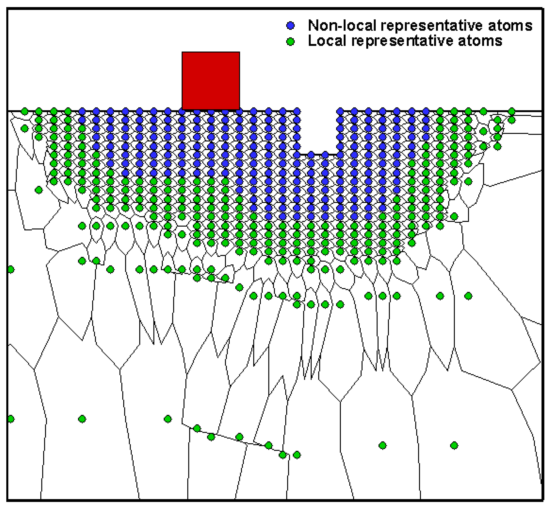
2. Methodology
3. Results
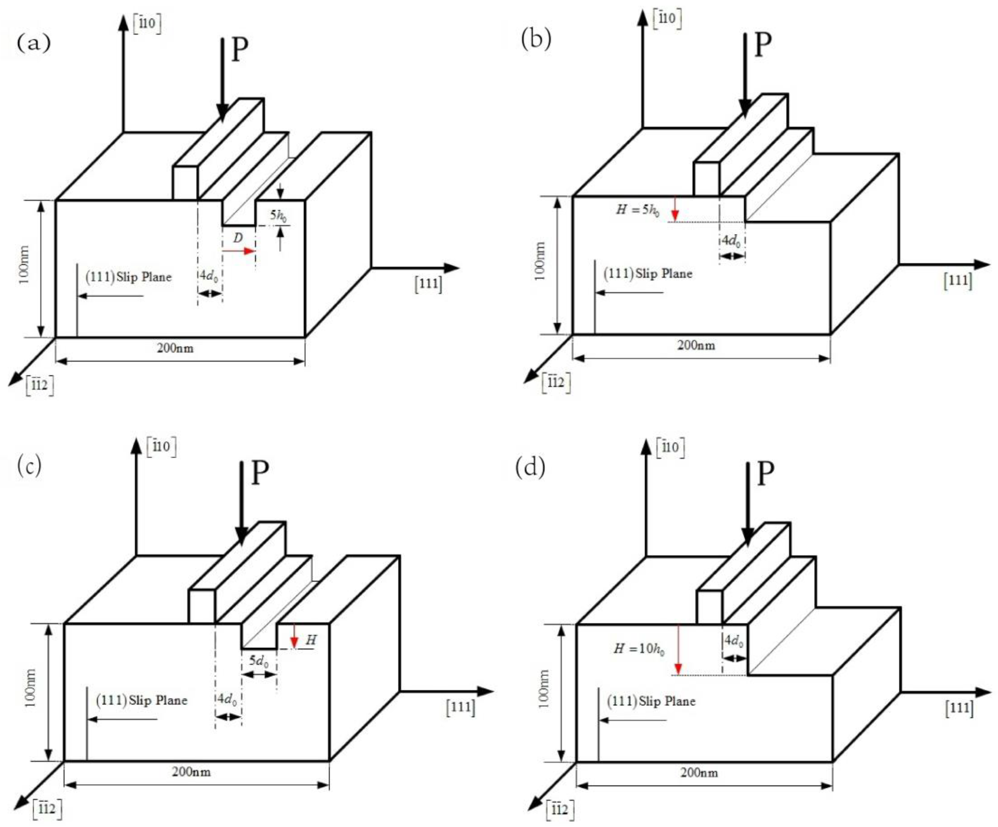
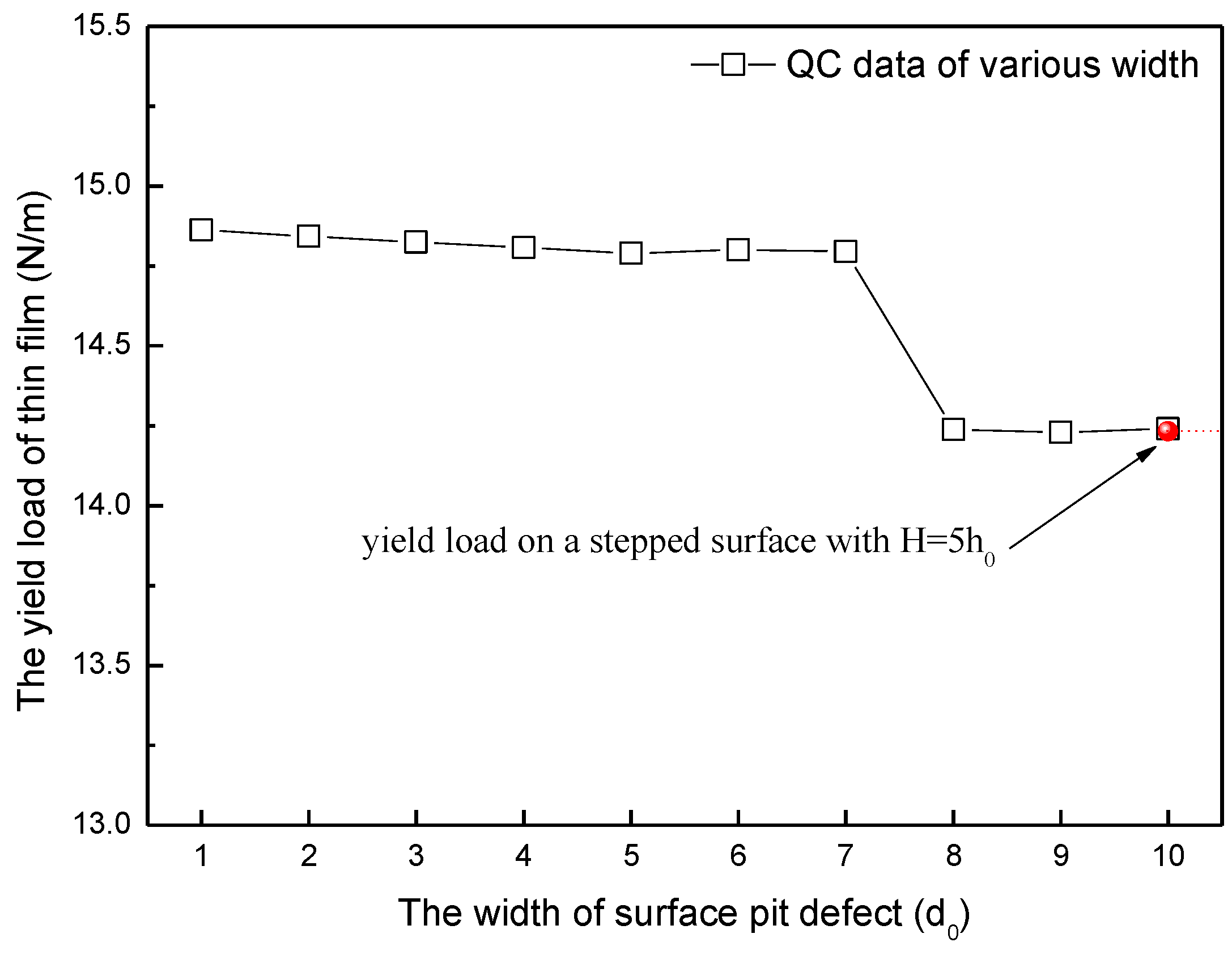
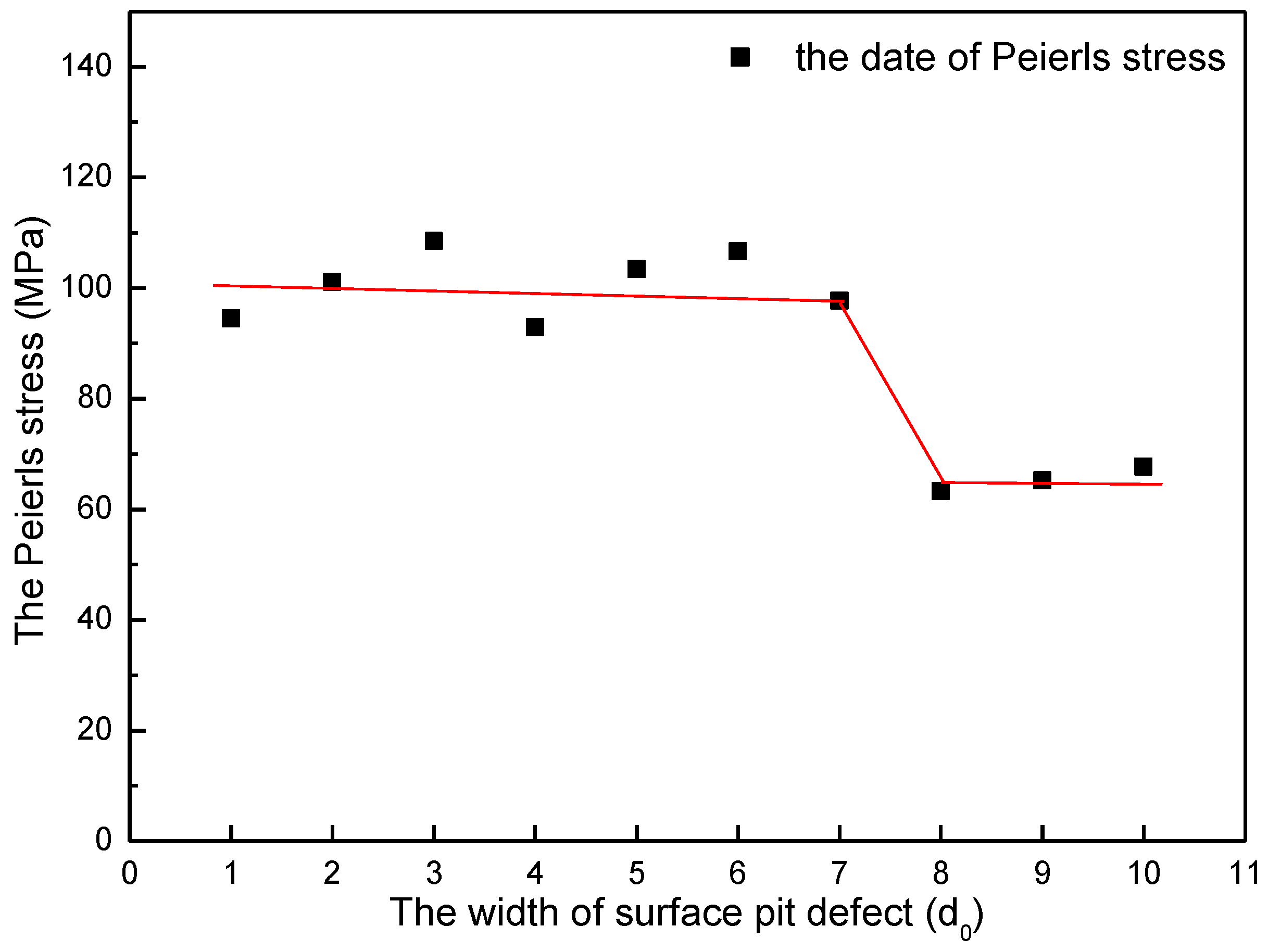
3.1. Width Effect of Surface Pit Defect on Yield Load
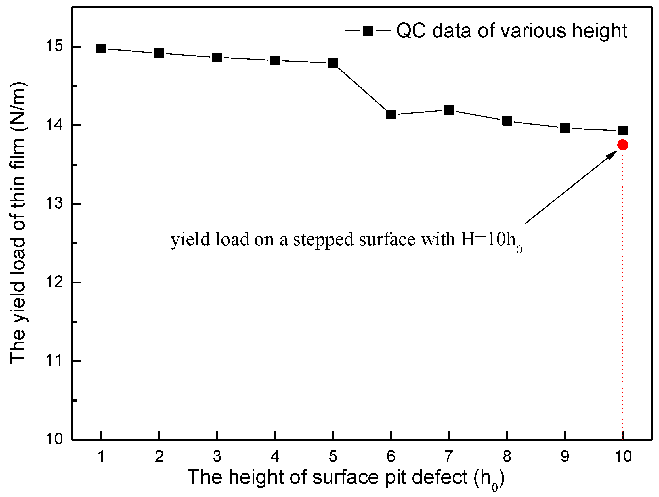
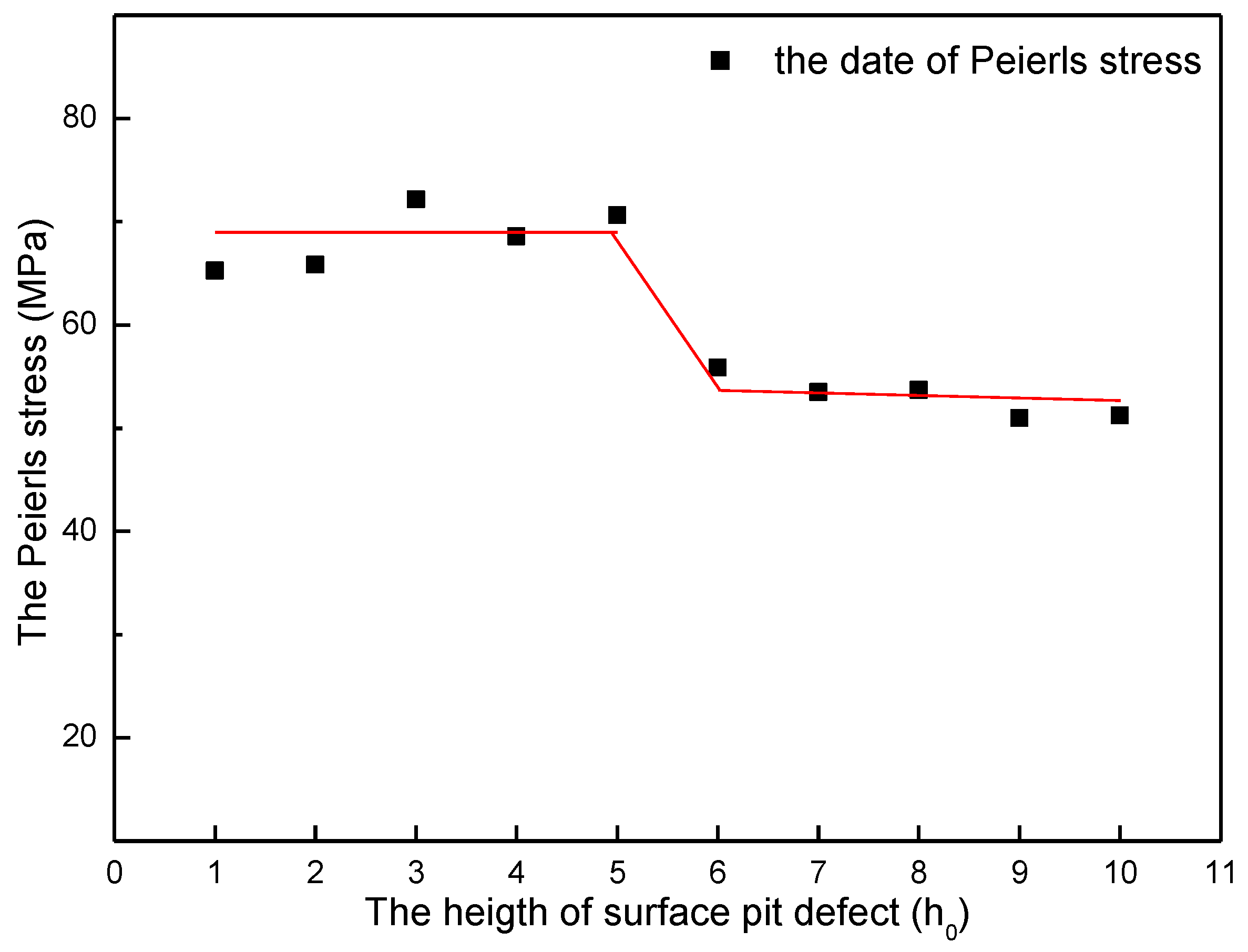
3.2. Height Effect of Surface Pit Defect on Yield Load
4. Discussion
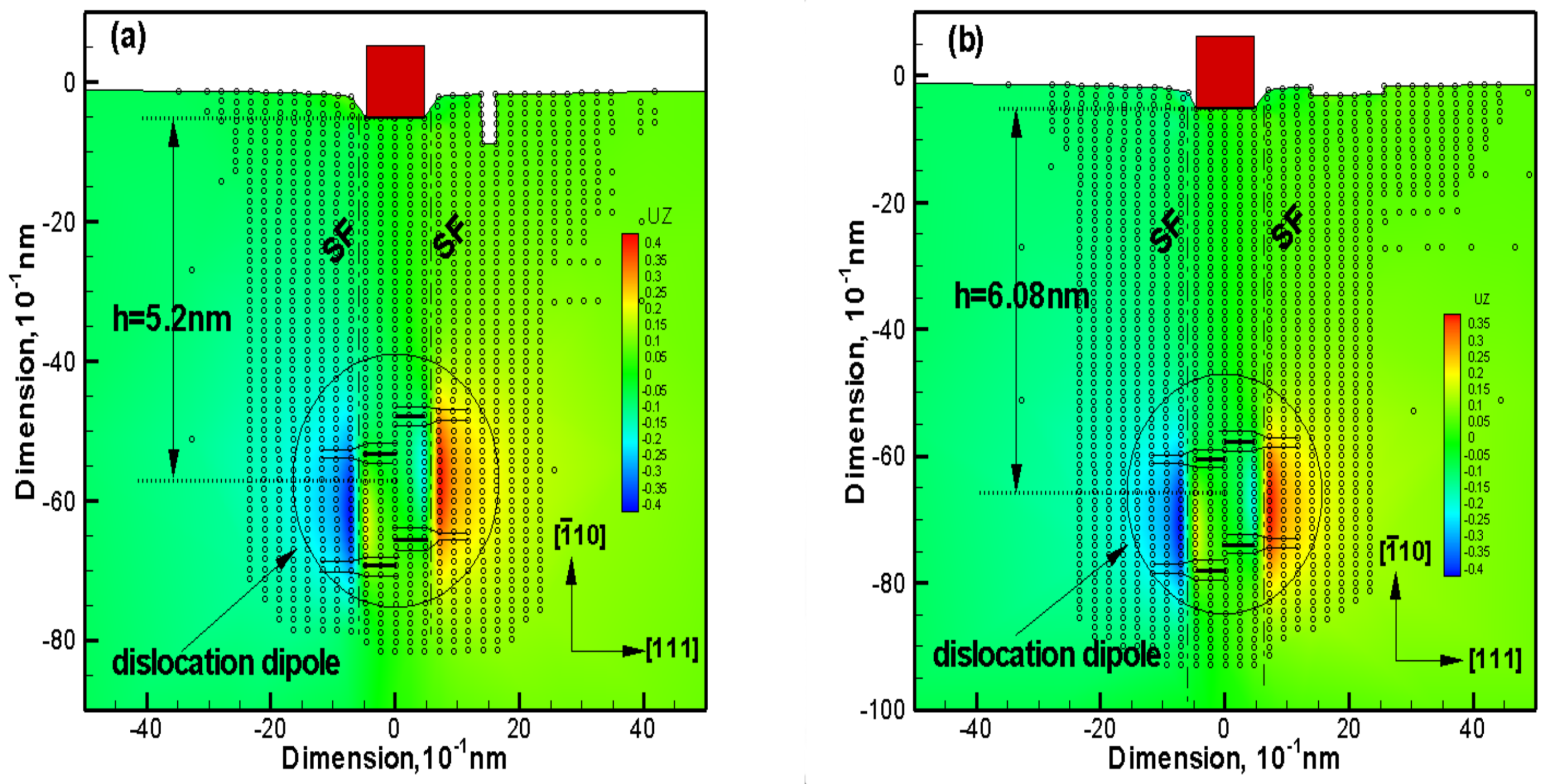
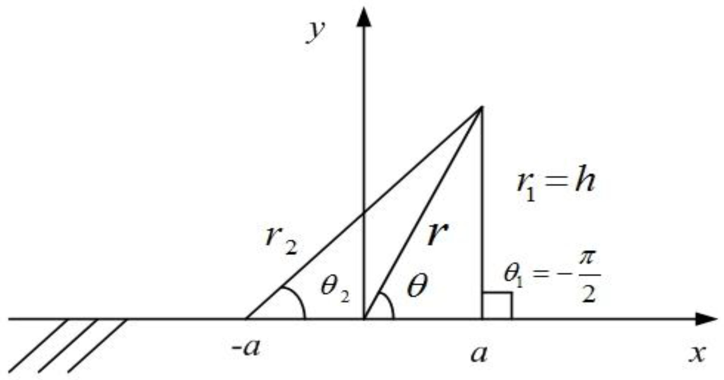
4.1. The Investigation of Dislocation Nucleation and the Estimation of Peierls Stress
4.2. Size Coefficient
5. Conclusions
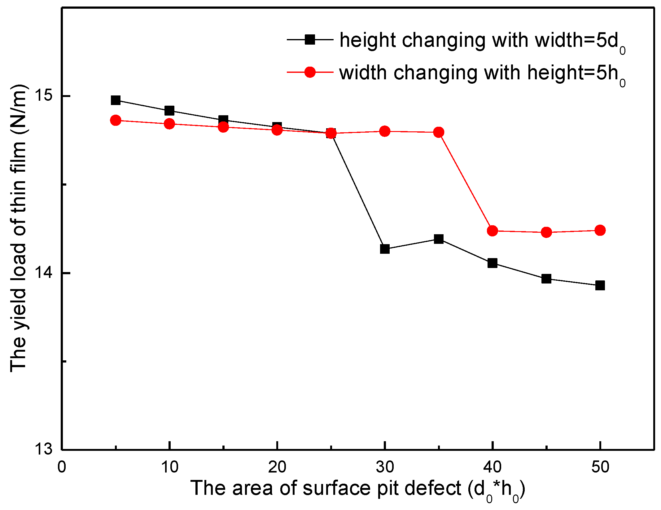
- As the width of surface pit defect increases, the yield load of thin film decreases extremely slowly, until the size coefficient of width equals approximately one unit, at which point the yield load experiences an obvious drop. When the size coefficient of width reaches approximately two units, the yield load is almost the same as that of the nanoindentation on a stepped surface.
- As the height of surface pit defect increases, the yield load of thin film decreases extremely slowly, until the size coefficient of height equals approximately half unit, at which point the yield load experiences an obvious drop. When the size coefficient of height reaches one unit, the yield load is almost the same as that of the nanoindentation on a stepped surface.
- The height of surface pit defect has more influence than the width on the yield load of thin film, which suggests that the height of the pit is a leading factor on the influence of yield load. Such investigation results in this simulation may have important directive to the defects testing or material application.
Author Contributions
Acknowledgments
Conflicts of Interest
References
- Oliver, W.C.; Pharr, G.M. An improved technique for determining hardness and elastic modulus using load and displacement sensing indentation experiments. J. Mater. Res. 1992, 7, 1564–1583. [Google Scholar] [CrossRef]
- Mitchell, J.W. Growth and Perfection of Crystals; Doremus, R.H., Roberts, B.W., Turnbull, D., Eds.; Wiley: New York, NY, USA, 1958; pp. 386–389. [Google Scholar]
- Yang, B.; Vehoff, H. Dependence of nanohardness upon indentation size and grain size—A local examination of the interaction between dislocations and grain boundaries. Acta Mater. 2007, 55, 849–856. [Google Scholar] [CrossRef]
- Soifer, Y.M.; Verdyan, A.; Kazakevich, M.; Rabkin, E. Nanohardness of copper in the vicinity of grain boundaries. Scr. Mater. 2002, 47, 799–804. [Google Scholar] [CrossRef]
- Griffith, A.A., VI. The phenomena of rupture and flow in solids. Philos. Trans. R. Soc. Lond. A 1921, 221, 163. [Google Scholar] [CrossRef]
- Shan, D.; Yuan, L.; Guo, B. Multiscale simulation of surface step effects on nanoindentation. Mater. Sci. Eng. A 2005, 412, 264–270. [Google Scholar] [CrossRef]
- Kiey, J.D.; Hwang, R.Q.; Houston, J.E. Effect of Surface Steps on the Plastic Threshold in Nanoindentation. Phys. Rev. Lett. 1998, 81, 4424–4427. [Google Scholar]
- Pogorelko, V.V.; Krasnikov, V.S.; Mayer, A.E. High-speed collision of copper nanoparticles with aluminum surface: Inclined impact, interaction with roughness and multiple impact. Comput. Mater. Sci. 2018, 142, 108–121. [Google Scholar] [CrossRef]
- Santos, T.G.; Inácio, P.L.; Costa, A.A.; Miranda, R.M.; de Carvalho, C.C.C.R. Applications of a new NDT technique based on bacterial cells. NDT E Int. 2016, 78, 20–28. [Google Scholar] [CrossRef]
- Xu, F.L.; Xin, Y.S.; Li, T.S. Friction-induced surface textures of liquid crystalline polymer evaluated by atomic force microscopy, spectroscopy and nanoindentation. Polym. Test. 2018, 68, 146–152. [Google Scholar] [CrossRef]
- Erinosho, M.F.; Akinlabi, E.T.; Johnson, O.T. Characterization of surface roughness of laser deposited titanium alloy and copper using AFM. Appl. Surf. Sci. 2018, 435, 393–397. [Google Scholar] [CrossRef]
- Pei, H.Q.; Wen, Z.X.; Li, Z.W.; Zhang, Y.M.; Yue, Z.F. Influence of surface roughness on the oxidation behavior of a Ni-4.0Cr-5.7Al single crystal superalloy. Appl. Surf. Sci. 2018, 440, 790–803. [Google Scholar] [CrossRef]
- Tromas, C.; Stinville, J.C.; Templier, C.; Villechaise, P. Hardness and elastic modulus gradients in plasma-nitrided 316L polycrystalline stainless steel investigated by nanoindentation tomography. Acta Mater. 2012, 60, 1965–1973. [Google Scholar] [CrossRef]
- Mao, W.G.; Shen, Y.G.; Lu, C. Nanoscale elastic–plastic deformation and stress distributions of the C plane of sapphire single crystal during nanoindentation. J. Eur. Ceram. Soc. 2011, 31, 1865–1871. [Google Scholar] [CrossRef]
- Chang, T.R.; Tsai, C.H. Mechanical responses of Zn1-xMnxO epitaxial thin films. Appl. Surf. Sci. 2011, 258, 614–617. [Google Scholar] [CrossRef]
- Li, K.; Morton, K.; Veres, T.; Cui, B. Nanoimprint Lithography and Its Application in Tissue Engineering and Biosensing. Compr. Biotechnol. 2011, 5, 125–139. [Google Scholar]
- Park, S.Y.; Choi, K.B.; Lim, H.J.; Lee, J.J. Fabrication of a nano-scale embedded metal electrode in flexible films by UV/thermal nanoimprint lithography tools. Microelectron. Eng. 2011, 88, 1606–1609. [Google Scholar] [CrossRef]
- Taylor, H.; Smistrup, K.; Boning, D. Modeling and simulation of stamp deflections in nanoimprint lithography: Exploiting backside grooves to enhance residual layer thickness uniformity. Microelectron. Eng. 2011, 88, 2154–2157. [Google Scholar] [CrossRef]
- Jiang, W.G.; Su, J.J.; Feng, X.Q. Effect of surface roughness on nanoindentation test of thin films. Eng. Fract. Mech. 2008, 75, 4965–4972. [Google Scholar] [CrossRef]
- Li, J.W.; Ni, Y.S.; Lin, Y.H.; Luo, C. Multiscale simulation of nanoindentation on Al thin film. Acta Metall. Sin. 2009, 45, 129–136. [Google Scholar]
- Tadmor, E.B. The Quasicontinuum Method. Ph.D. Thesis, Brown University, Providence, RI, USA, 1996. [Google Scholar]
- Daw, M.S.; Baskes, M.I. Semiempirical, Quantum Mechanical Calculation of Hydrogen Embrittlement in Metals. Phys. Rev. Lett. 1983, 50, 1285. [Google Scholar] [CrossRef]
- Tadmor, E.B.; Miller, R.; Phillips, R.; Ortiz, M. Nanoindentation and incipient plasticity. J. Mater. Res. 1999, 14, 2233–2250. [Google Scholar] [CrossRef]
- Muskhelishvili, N.I. Some Basic Problems of the Mathematical Theory of Elasticity, 3rd ed.; P. Noordhoff Ltd.: Groningen, The Netherlands, 1953; pp. 481–483. [Google Scholar]


© 2018 by the authors. Licensee MDPI, Basel, Switzerland. This article is an open access article distributed under the terms and conditions of the Creative Commons Attribution (CC BY) license (http://creativecommons.org/licenses/by/4.0/).
Share and Cite
Zhang, Z.; Ni, Y.; Zhang, J.; Wang, C.; Ren, X. Multiscale Analysis of Size Effect of Surface Pit Defect in Nanoindentation. Micromachines 2018, 9, 298. https://doi.org/10.3390/mi9060298
Zhang Z, Ni Y, Zhang J, Wang C, Ren X. Multiscale Analysis of Size Effect of Surface Pit Defect in Nanoindentation. Micromachines. 2018; 9(6):298. https://doi.org/10.3390/mi9060298
Chicago/Turabian StyleZhang, Zhongli, Yushan Ni, Jinming Zhang, Can Wang, and Xuedi Ren. 2018. "Multiscale Analysis of Size Effect of Surface Pit Defect in Nanoindentation" Micromachines 9, no. 6: 298. https://doi.org/10.3390/mi9060298
APA StyleZhang, Z., Ni, Y., Zhang, J., Wang, C., & Ren, X. (2018). Multiscale Analysis of Size Effect of Surface Pit Defect in Nanoindentation. Micromachines, 9(6), 298. https://doi.org/10.3390/mi9060298