Article

Investigation of Micro Square Structure Fabrication by Applying Textured Cutting Tool in WEDM

Engineering Research Center of Extreme Precision Optics, State Key Laboratory of Applied Optics, Changchun Institute of Optics, Fine Mechanics and Physics, Chinese Academy of Science, Changchun 130033, China
*
Author to whom correspondence should be addressed.
Micromachines 2015, 6(10), 1427-1434; https://doi.org/10.3390/mi6101427
Submission received: 7 August 2015 / Revised: 29 August 2015 / Accepted: 17 September 2015 / Published: 25 September 2015

Abstract

:
This paper studies micro structure fabrication by means of a textured tool cutting edge, which is manufactured by applying the wire cut electrical discharge machining (WEDM). Machining performance of the square structure fabrication on the tool cutting edge is investigated in the WEDM process, and the machining accuracy is explored in experimental analyses. In this proposed method, undesired overcut comes from the discharge between the processing debris and the side wall of the target structure. Furthermore, by applying the textured cutting tool, the target square structure is directly fabricated on the alumina workpiece with just a simple turning process, which verifies the feasibility of the proposed tool cutting edge textured method by applying the WEDM. This technology is expected to become a potential method for the mass production of micro structure surfaces in the future.

1. Introduction

Structured surfaces with sophisticated micro/nano structures can provide advanced and useful functions. These micro/nano-structured surfaces can exhibit a number of novel and excellent functions and features as compared with just simple smooth surfaces. To achieve the maximum benefit from the structured surfaces, application technologies of the micro/nano-structured surfaces have been a fascinating research topic in the last few decades. Structured surfaces have been increasingly demanded in various applications, such as optics [1], solar energy technology [2], bioengineering [3], self-cleaning [4], manufacturing [5,6], and so on [7]. To promote widespread use of structured surfaces, their applications and their mass production, manufacturing technology of structured surfaces for a variety of materials is absolutely essential. Numerous fabrication methods for micro/nano structure have been proposed so far. Typical methods for micro/nano structure fabrication are proposed, including lithographic machining, laser beam machining, focused ion beam machining, electron beam machining, diamond machining, electrical discharge machining, and so on.
Lithography, focused ion beam machining and electron beam machining play a critical role in micro/nano-structure fabrication. These processes are advantageous in fabricating highly-dense micro/nano structures with a high aspect ratio and straight sidewalls. The feature size can be downscaled into tens of nanometers or even several single nanometers. However, these manufacturing technologies are not available for a large structure height of several hundred micrometers due to their low removal rate and time-consuming nature. Considering the mechanical micromachining technologies, micro grinding is not available for dense micro/nano structure fabrication due to the size restriction of grinding wheel, especially the radius of the wheel tip. Diamond cutting has a large dimension span in micro/nano structure fabrication, which is flexible and capable of many different designs. However, diamond cutting is usually applied to the fabrication of precision parts on limited plastic materials, such as soft metals including oxygen-free copper, brass, aluminum alloy, polymeric material such as polymethyl methacrylate, electroless nickel-phosphorus plating [8], and so on. However, conventional diamond cutting is not applicable directly to steel materials due to extreme chemical tool wear [9]. Moreover, it is difficult to apply diamond cutting technology to hard and brittle materials machining because of the tool edge chipping and machined surface deterioration [10,11]. Recently, Wire-cut Electrical Discharge Machining (WEDM) is considered as one of the effective methods for the machining of difficult-to-cut materials. The WEDM can be applied for the machining of electrically conductive materials. This machining technology uses the instant high temperature of spark discharge to melt or vaporize the workpiece. It is also suitable for hard and brittle materials machining because of its very small macroscopic mechanical force [12,13,14]. The fracture propagation can be reduced efficiently inside the workpiece material. Moreover, Masuzawa et al. [15] reported using WEDM to machine cylindrical parts for manufacturing small pins. Miniature electrodes and micro-structures were also successfully fabricated with this technique [16]. Hence, the WEDM is expected to be a kind of potential method for simple micro structure fabrication on electrically conductive materials.
Furthermore, according to tribological applications, the friction between sliding surfaces may be reduced effectively by texturing in a micrometer scale. The micro-structures could be regarded as a set of micro-bearings distributed over the sliding surface [17,18]. They can offer excellent tribological performances because of the improvement of lubrication and the enhancement of a hydrodynamic pressure due to the constituted converging wedges. Micro structures fabricated on the tool cutting edge may expose the surrounding gas and/or the cutting fluid into the contact surfaces of the cutting edge and the workpiece, resulting in cooling of the tool and workpieces. Micro structures fabricated on the tool cutting edge may improve cutting performances.
For the mass production of micro structure surfaces, this paper introduces a micro structure manufacturing technology on the tool cutting edge by applying a WEDM process. Firstly, the machining process is introduced. The target micro structure is fabricated on the cutting edge, and then the envelop of the cutting edge is directly transferred into the workpiece in the turning process. The efficiency of the micro structure fabrication can be increased by applying the proposed method. Following that, the generation of machining error is explored in experimental analyses. The machining accuracy deterioration mainly comes from the discharge between the processing debris and the side wall of the target structure in WEDM process. Finally, the tool wear/damage is also investigated. Intermittent contact of the cutting tool with the workpiece may occasionally cause local stress concentration at the cutting edge, resulting in micro chipping/breakage. Consequently, cumulative chipping/breakage on the cutting edge may develop into serious tool damage.

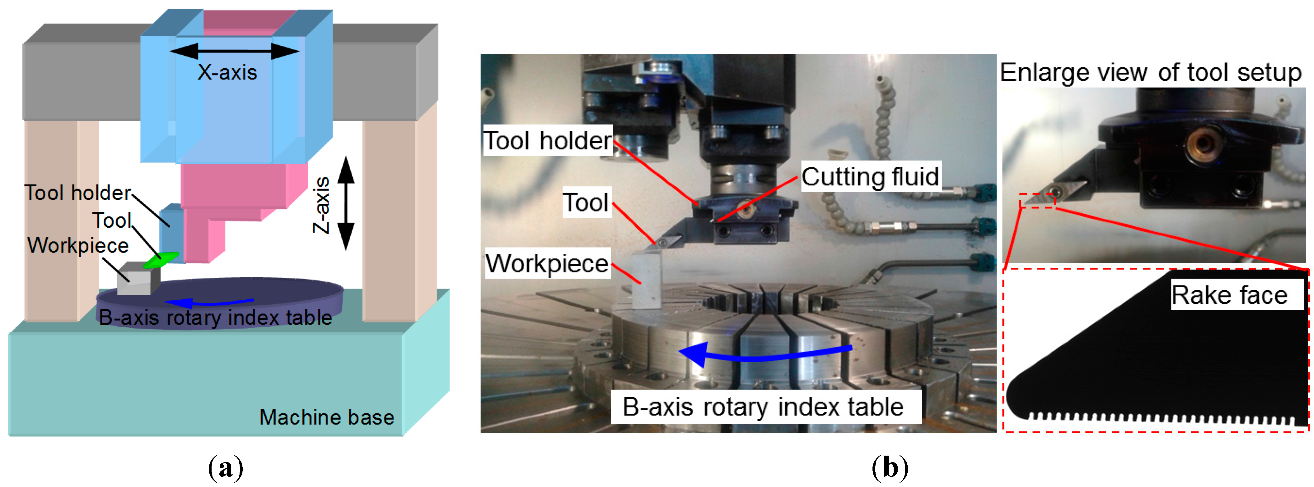
2. Experimental Conditions and Experimental Setup

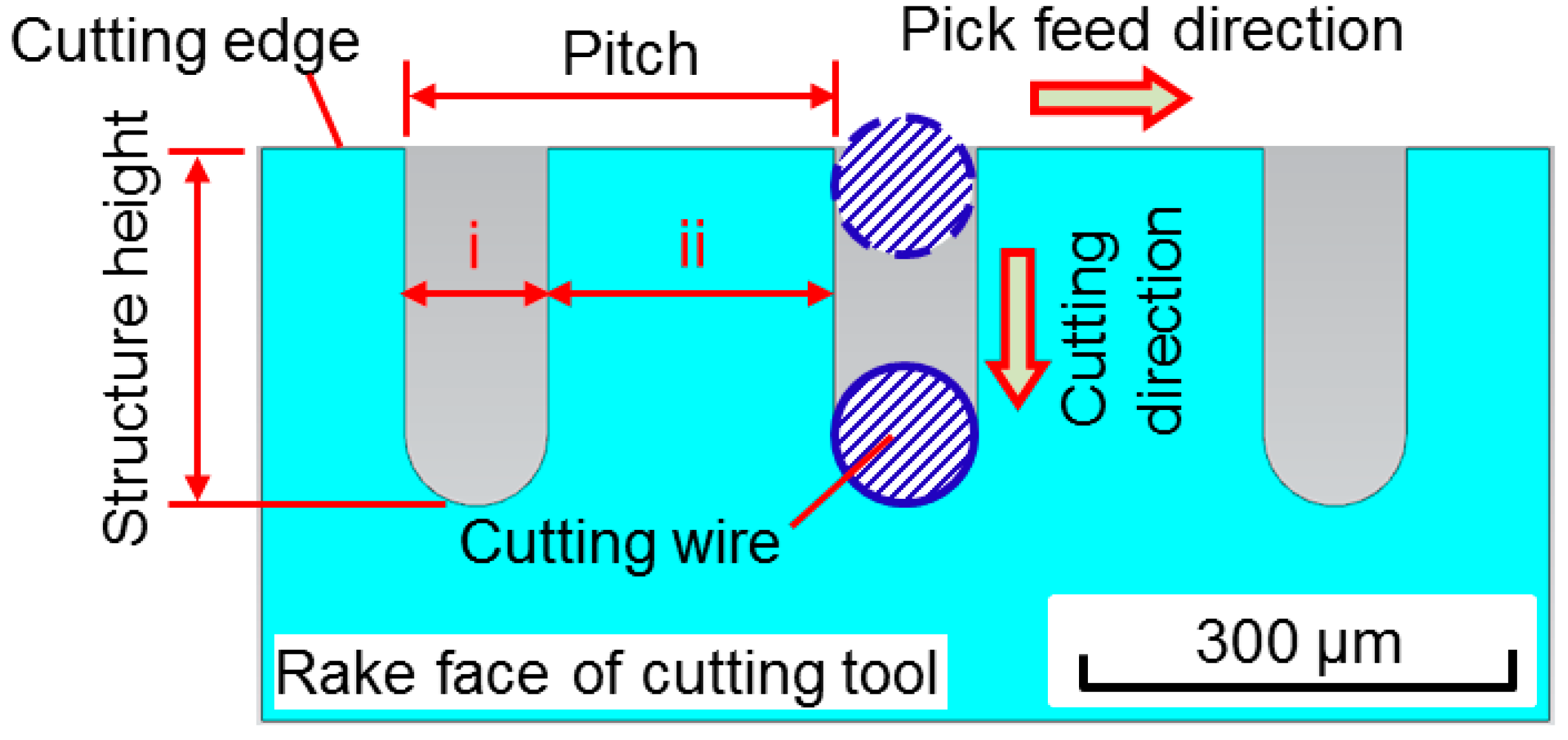
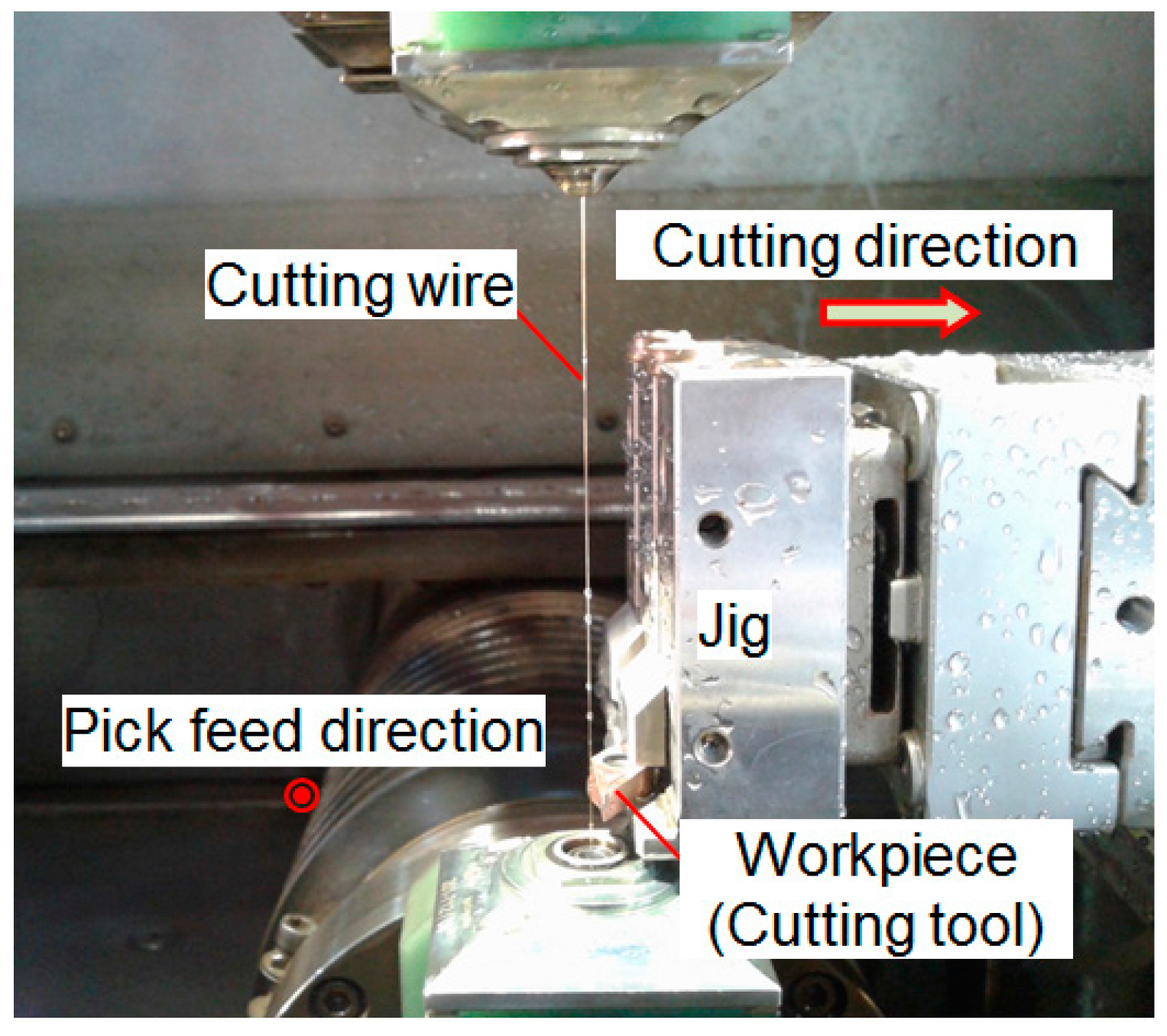
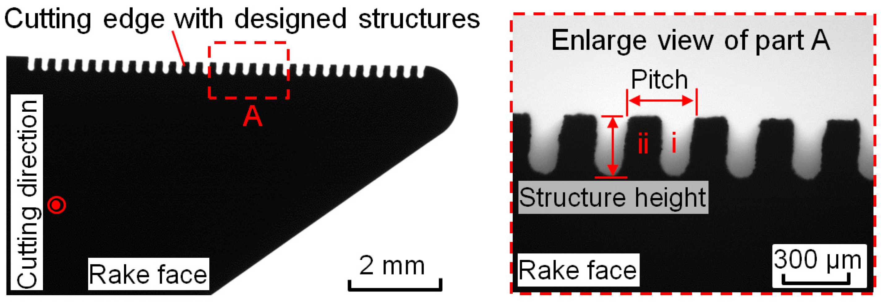
2.1. Target Structure Fabrication on Tool Cutting Edge

A cutting tool with a nose radius of 0.8 mm, a clearance angle of 5° and a rake angle of 0° is used in the experimental investigations. The tool is made of cemented carbide and fabricated by SANDVIK Co., Ltd. (Sandviken, Sweden). In the WEDM process, the cutting wire is made of CuZn37 coated with special layer (AC Cut AH), which is fabricated by Agie Charmilles Co., Ltd. (Geneva, Switzerland). The radius of the cutting wire is 50 μm. Considering the size restrictions in machinable part geometry, i.e., the radius of the cutting wire and the kinematic accuracy of the machine tools, a series of simple textured grooves with a structure height of 250 μm and a pitch value of 300 μm are designed on the tool cutting edge, as shown in Figure 1. The feed ratio along the cutting direction is set to be 100 mm/min. The pick feed value is equal to the designed pitch value of 300 μm. The width of part i is designed as 100 μm and 200 μm in part ii, as Figure 1 shows. The feasibility of micro square structure fabrication on the tool cutting edge is investigated by applying the WEDM technology.
Figure 2 shows the experimental setup for texturing the tool cutting edge. A precision WEDM machine called Agie Charmilles CUT3000 is used. The cutting wire is set to be vertical to the tool cutting edge.
Figure 1. Designed target structure on cutting tool cutting edge.
Micromachines 06 01427 g001
Figure 2. Experimental setup for texturing the tool cutting edge.
Micromachines 06 01427 g002

2.2. Micro Structure Fabrication in Turning Process

Following that, the target micro structure is fabricated on the aluminum alloy (Al6061) by applying the textured cutting tool. The experimental setup is shown in Figure 3. A precision machine tool Microturn 1000V made by HEMBRUG Machine Tool Corp (Haarlem, The Netherlands) is used for the target structure fabrication. A positioning resolution of linear axes is 10 nm. The workpiece is fixed to the top surface of B-axis, the rotation velocity of which is set to be 20 rpm. The nominal cutting speed is calcuated as about 1 m/min at the workpiece fixed position. The tool cutting edge is set to be along the horizontal direction and the rake face of the cutting tool is vertical to the cutting direction. The cutting tool is fed along the depth of cut direction by controlling the motion of Z-axis. The depth of cut linearly increases with the value of 10 μm/rpm, and the final depth of cut is designed as 200 μm. The width of the cutting regime is a little smaller than the length of tool cutting edge. The envelop of cutting edge is then directly transferred into the workpiece in the simple turning process.
Figure 3. (a) Illustration and (b) picture of experimental setup for micro structure fabrication in turning process.
Micromachines 06 01427 g003

3. Analysis of Experimental Results

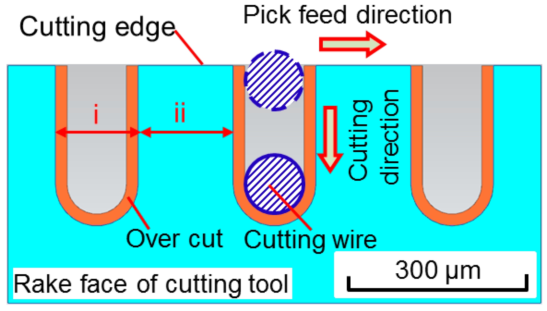
3.1. Micro Structure Fabrication on Tool Cutting Edge by Applying WEDM

As Figure 2 shows, the target square wave structure is fabricated on the tool cutting edge by applying the WEDM. The machined structure was subsequently examined by using an optical microscope. Figure 4 shows the machining results, where the average measured structure height is 263.2 μm and the average measured pitch value is 299.6 μm.
The pitch value is almost equal to the designed value of 300 μm because of the stable feed value of the precision WEDM machine tool. However, the structure height is larger than the designed value of 250 μm. This machining error may be caused by the overcut in the EDM process. The discharge between the processing debris and the side wall of the target structure may result in the over removing of workpiece material, as shown in Figure 5. This phenomenon causes undesired space between the WEDM cutting wire and the target structure, resulting in the deterioration of machining accuracy. Due to the reaction between the cutting wire and the side surface of target structure, the overcut occurs. Consequently, Figure 5 shows that the width of part ii (about 163.2 μm) is also not exactly two times the width valve of part i (about 126.8 μm), as was the case in Figure 1. Due to the experimental investigations, the effective radius of cutting wire can be obtained as 63.4 μm in the WEDM process. In the future, the relationship between the material remove ratio and the discharge time should be evaluated in order to improve the machining accuracy. In this paper, we mainly focus on the feasibility of micro structure fabrication by the proposed method. Through the experimental verifications, it was confirmed that the micro structure can be efficiently fabricated on the cemented carbide tool cutting edge by applying the WEDM process.
Figure 4. Machined micro structures on tool cutting edge by applying wire cut electrical discharge machining (WEDM).
Micromachines 06 01427 g004
Figure 5. Illustration of over cut generation in WEDM process.
Micromachines 06 01427 g005

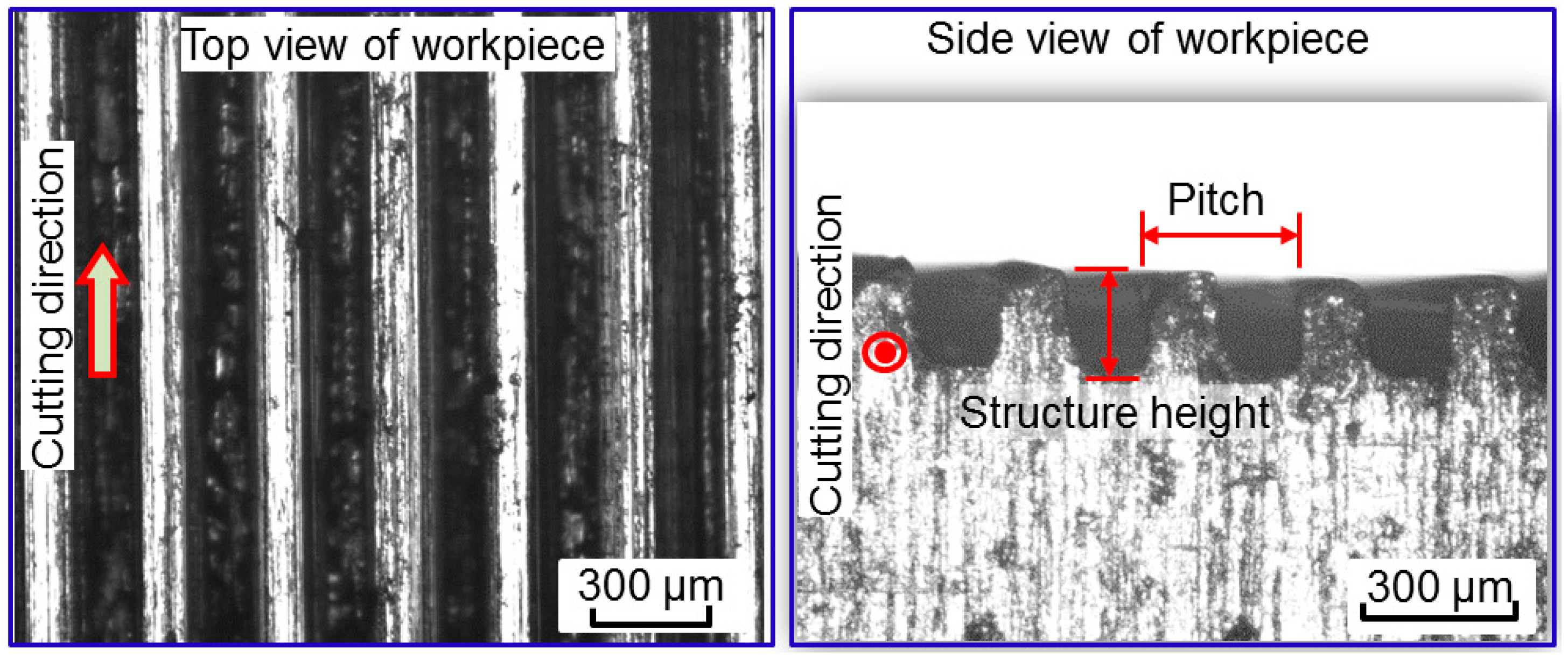
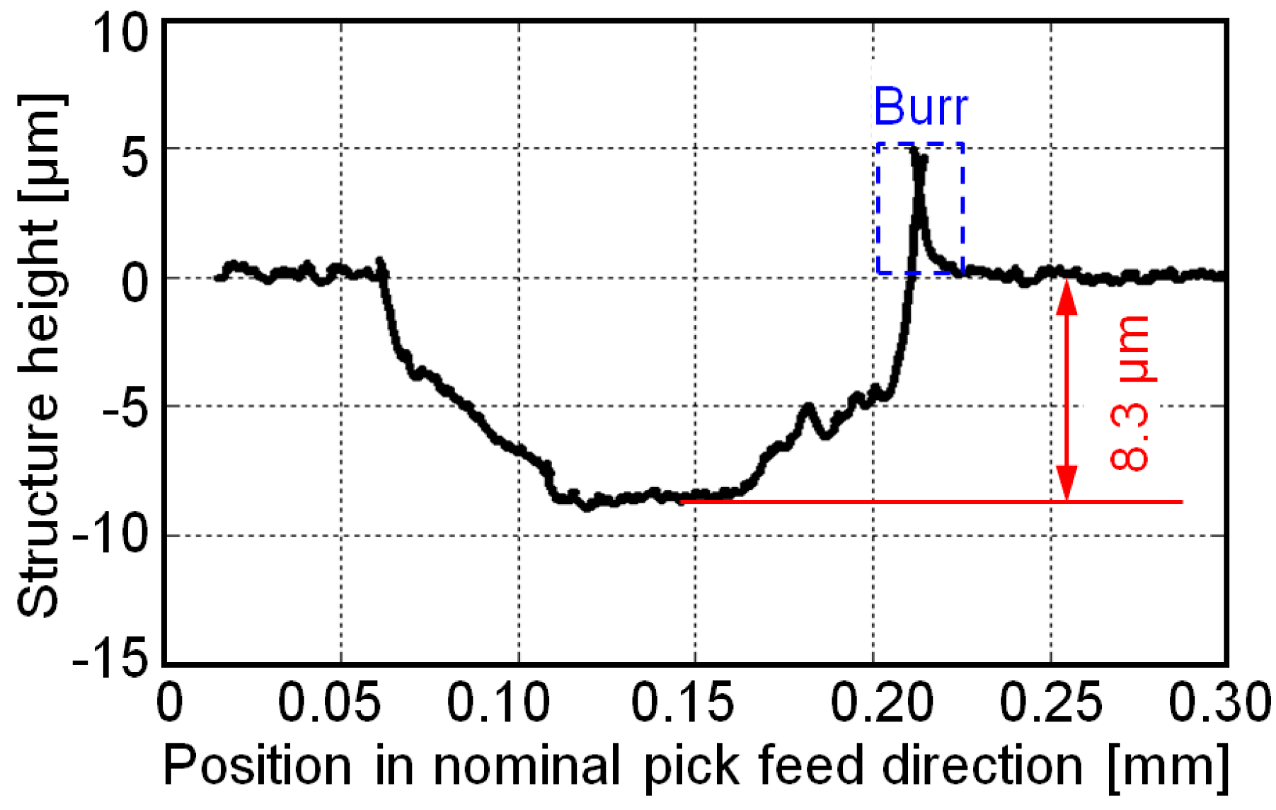
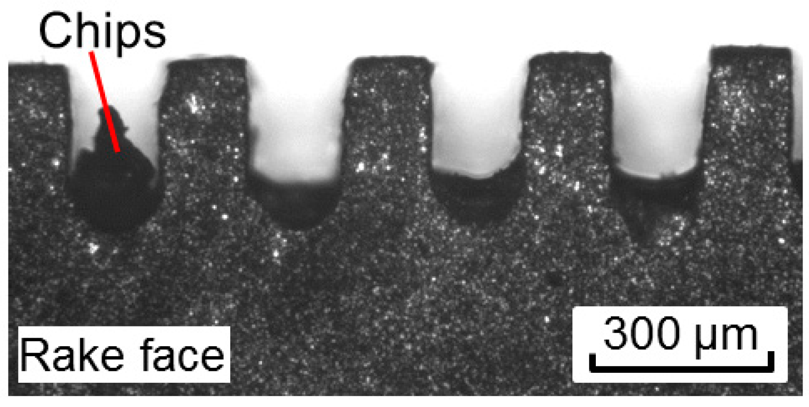
3.2. Micro Structure Fabrication on Aluminum Alloy by Applying the Textured Cutting Tool

Following that, the textured cutting tool is applied to the fabrication of micro square structures in the simple turning process. As Figure 3 shows, the depth of cut is linearly increased to 200 μm. Figure 6 shows the machining results, where the average measured structure height is 197.6 μm and the average measured pitch value is 299.2 μm.
The pitch value is almost equal to the pitch value of the fabricated micro structure on the tool cutting edge. However, the structure height is smaller than the designed value of 200 μm. Based on Ramos’s report [19], the radius of cutting edge is several micrometers in a new cemented carbide cutting tool. The edge radius of the textured cutting tool is measured by an optical microscope (Bruker NPFLEX, Billerica, MA, USA) after the WEDM process. In advance of the measurement, the tool edge is carefully cleaned with acetone. The measured value of the tool edge radius is about 8.8 μm. In the present research, the intermittent turning process is adopted, as shown in Figure 3. The depth of the cut is 10 μm in each cutting. As the edge radius of the cutting tool is comparable in size to the depth of cut, this reduced sharpness may have a certain influence on the machining accuracy deterioration in micro scale machining.
In order to evaluate the machining accuracy in the present micro machining process, the micro square structure is fabricated again by applying only one turning pass. The depth of cut stays at 10 μm. One pitch of the fabricated square structures is investigated. Figure 7 shows a cross section profile of the square groove, which is measured by using a surface profiler (Taylor Hobson PGI 1250S, Leicester, UK).
Figure 6. Machined micro structures on aluminum alloy by applying textured cutting tool.
Micromachines 06 01427 g006
Figure 7. Cross section profile of one square groove.
Micromachines 06 01427 g007
It should be noted that the sharp corner at the bottom of the square groove may not be machined precisely because of the elastic/plastic deformation of the workpiece material. Moreover, the radius of diamond stylus used for the measurement process is about 2.5 μm. Due to the radius of the diamond stylus, the sharp corner also cannot be exactly measured. In this section, the machining accuracy along the depth of cut direction is primarily investigated. Although the chip formation can be observed during the cutting process, the machined structure height of about 8.3 μm is smaller as compared with the depth of cut of 10 μm. The plastic recovery of workpiece material takes place at the bottom of the square groove. As the depth of cut is just a little larger than the edge radius of cutting tool, the motion of workpiece material being pushed may be huge at the bottom of the cutting edge. This pushing process may also cause the burr generation in micro machining of the square groove. Malekian et al. [20] clarified that the minimum uncut chip thickness in micro machining of aluminum (Al6061) is about 0.23re, where re is the edge radius of cutting tool. Below the minimum uncut chip thickness, the cutting process is dominated by a ploughing process, which is a type of plastic deformation of the workpiece material without chip formation. The ploughing process causes the increase of edge force and the deterioration of finished surface quality. It should be noted that the uncut chip thickness is the same as the depth of cut in this present research. Based on Malekian’s research results, the ploughing process is dominant when the depth of cut is smaller than about 2 μm in this research. Because the depth of cut is not much larger than the minimum uncut chip thickness of 2 μm, large edge force may be generated in the cutting process. Consequently, the plastic deformation of the fabricated structure may increase the machining error in the depth of cut direction.
After the experiments, part of the used tool cutting edge is measured by using an optical microscope. In advance of the measurement, the tool cutting edge is carefully cleaned with acetone. Figure 8 shows a measurement result of the used cutting edge, where considerable adhesion of the chips/workpiece material can be observed in the fabricated micro structures. This phenomenon may cause the increasing of adhesion wear, resulting in the increasing of tool edge radius and edge forces. As shown in Figure 8, the geometry of the fabricated micro structure on the tool cutting edge remains almost stable after the experiment.
Figure 8. Used tool cutting edge after the experiment.
Micromachines 06 01427 g008
However, the tool damage is obviously generated on another part of the used tool cutting edge, as shown in Figure 9. In the present research, a small size aluminum alloy workpiece is adopted in the turning process. The cutting tool contacts with the workpiece in each rotation cycle of the B-axis, as shown in Figure 3. As compared with the common continues turning process, an intermittent turning process, which is similar to the fly-cutting process, is adopted in the present research. The tool damage is considered to be due to the accumulation of intermittent contact of the cutting edge to the workpiece material. Despite the hardness of cemented carbide being relatively higher than that of aluminum alloy material, intermittent contact may occasionally cause local stress concentration at the tool cutting edge with the micro structure, which results in the tool edge breakage. Furthermore, cemented carbide particles apart from the cutting edge may be extremely hard and abrasive. These hard particles of the tool material can scratch the flank face side of the cutting edge and/or accelerate further breakage generation. Consequently, cumulative chipping and breakage on the flank face may develop into the serious tool damages shown in Figure 9.
Figure 9. Used tool cutting edge with damaged part.
Micromachines 06 01427 g009

4. Conclusions

Based on the experimental study, it is confirmed that practical micro square structure fabrication is feasible by means of the textured cutting tool in the WEDM process. The target structure is firstly fabricated on the tool cutting edge by applying the WEDM. Then, the envelop of the cutting edge is directly transferred into the workpiece in a turning process. By applying the proposed method, the machining error generation is experimentally explored when fabricating the target structure on the tool cutting edge. The machining accuracy deterioration mainly comes from the discharge between the processing debris and the side wall of the target structure in the WEDM process. After that, the tool wear/damage is also investigated. Intermittent contact of the cutting tool with the workpiece may occasionally cause local stress concentration at the tool cutting edge, resulting in micro breakage. Consequently, cumulative breakage and/or chipping may develop into serious tool damage. In order to increase the machining accuracy and decrease the tool wear/damage, much more research needs to be carried out in the future.

Acknowledgments

We acknowledge Agie Charmilles Co., Ltd., HEMBRUG Machine Tool Co., Ltd. and SANDVIK Co., Ltd. for their experimental support. We thank the National Basic Research Program of China (Grant No. 2009ZX02005) for the financial support.

Author Contributions

Jianguo Zhang, Quansong Li and Hui Zhang proposed and designed the experiments. They analyzed the experimental data and wrote the paper. Yongxin Sui and Huaijiang Yang provided their valuable guidance while working on this research project.

Conflicts of Interest

The authors declare no conflict of interest.

References

  1. Shieh, H.P.D.; Huang, Y.P.; Chien, K.W. Micro-optics components for liquid crystal displays applications. In Proceedings of the 24th International Display Research Conference, Daegu, Korea, 23–27 August 2004; pp. 56–58.
  2. Xie, W.T.; Dai, Y.J.; Wang, R.Z.; Sumathy, K. Concentrated solar energy applications using Fresnel lenses: A review. Renew. Sustain. Energy Rev. 2011, 15, 2588–2606. [Google Scholar] [CrossRef]
  3. Miyoshi, H.; Adachi, T.; Ju, J.; Lee, S.M.; Cho, D.J.; Ko, J.S.; Uchida, G.; Yamagata, Y. Characteristics of motility-based filtering of adherent cells on microgrooved surfaces. Biomaterials 2012, 33, 395–401. [Google Scholar] [CrossRef] [PubMed]
  4. Bico, J.; Marzolin, C.; Quéré, D. Pearl drops. Europhys. Lett. 1999, 47, 220–226. [Google Scholar] [CrossRef]
  5. Gao, W.; Dejima, S.; Kiyono, S. A dual-mode surface encoder for position measurement. Sens. Actuators A 2005, 117, 95–102. [Google Scholar] [CrossRef]
  6. Gao, W.; Kimura, A. A three-axis displacement sensor with nanometric resolution. CIRP Ann. Manuf. Technol. 2007, 56, 529–532. [Google Scholar] [CrossRef]
  7. Evans, C.J.; Bryan, J.B. “Structured”, “Textured” or “Engineered” surfaces. CIRP Ann. Manuf. Technol. 1999, 48, 541–556. [Google Scholar] [CrossRef]
  8. Yan, J.W.; Oowada, T.; Zhou, T.F.; Kuriyagawa, T. Precision machining of microstructures on electroless-plated NiP surface for molding glass components. J. Mater. Process. Technol. 2009, 209, 4802–4808. [Google Scholar] [CrossRef]
  9. Paul, E.; Evans, C.J.; Mangamelli, A.; McGlauflin, M.L.; Polvani, R.S. Chemical aspects of tool wear in single point diamond turning. Precis. Eng. 1996, 18, 4–19. [Google Scholar] [CrossRef]
  10. Bulla, B.; Klocke, F.; Dambon, O. Analysis on ductile mode processing of binderless nano crystalline tungsten carbide through ultra precision diamond turning. J. Mater. Process. Technol. 2012, 212, 1022–1029. [Google Scholar] [CrossRef]
  11. Yan, J.W.; Zhang, Z.Y.; Kuriyagawa, T. Mechanism for material removal in diamond turning of reaction-bonded silicon carbide. Int. J. Mach. Tools Manuf. 2009, 49, 366–374. [Google Scholar] [CrossRef]
  12. Pan, H.J.; Liu, Z.D.; Gao, L.; Qiu, M.B.; Tian, Z.Q. Study of small holes on monocrystalline silicon cut by WEDM. Mater. Sci. Semicond. Process. 2013, 16, 385–389. [Google Scholar]
  13. Zhao, Y.H.; Kunieda, M.; Abe, K. Study of EDM cutting of single crystal silicon carbide. Precis. Eng. 2014, 38, 92–99. [Google Scholar] [CrossRef]
  14. Tian, Y.; Qiu, M.B.; Liu, Z.D.; Tian, Z.J.; Huang, Y.H. Discharge cutting technology for specific crystallographic planes of monocrystalline silicon. Mater. Sci. Semicond. Process. 2014, 27, 546–552. [Google Scholar] [CrossRef]
  15. Masuzawa, T.; Fujino, M.; Kobayashi, K.; Suzuki, T.; Kinoshita, N. Wire electro-discharge grinding for micro-machining. CIRP Ann. Manuf. Technol. 1985, 34, 431–434. [Google Scholar] [CrossRef]
  16. Kuo, C.L.; Huang, J.D. Fabrication of series-pattern microdisk electrode and its application in machining micro-slit of less than 10 μm. Int. J. Mach. Tools Manuf. 2004, 44, 545–553. [Google Scholar] [CrossRef]
  17. Costa, H.L.; Hutchings, I.M. Hydrodynamic lubrication of textured steel surfaces under reciprocating sliding conditions. Tribol. Int. 2007, 40, 1227–1238. [Google Scholar] [CrossRef]
  18. Bruzzone, A.A.G.; Coata, H.L.; Lonardo, P.M. Advances in engineered surfaces for functional performance. CIRP Ann. Manuf. Technol. 2008, 57, 750–769. [Google Scholar] [CrossRef]
  19. Ramos, C.; Autenrieth, H.; Strauß, T.; Deuchert, M.; Hoffmeister, J.; Schulze, V. Characterization of the transition from ploughing to cutting in micro machining and evaluation of the minimum thickness of cut. J. Mater. Process. Technol. 2012, 212, 594–600. [Google Scholar] [CrossRef]
  20. Malekian, M.; Mostofa, M.G.; Park, S.S.; Jun, M.B.G. Modeling of minimum uncut chip thickness in micro machining of aluminum. J. Mater. Process. Technol. 2012, 212, 553–559. [Google Scholar] [CrossRef]

