
A Novel ANN-PSO Method for Optimizing a Small-Signal Equivalent Model of a Dual-Field-Plate GaN HEMT


 and
and
Abstract
1. Introduction
2. Materials and Methods
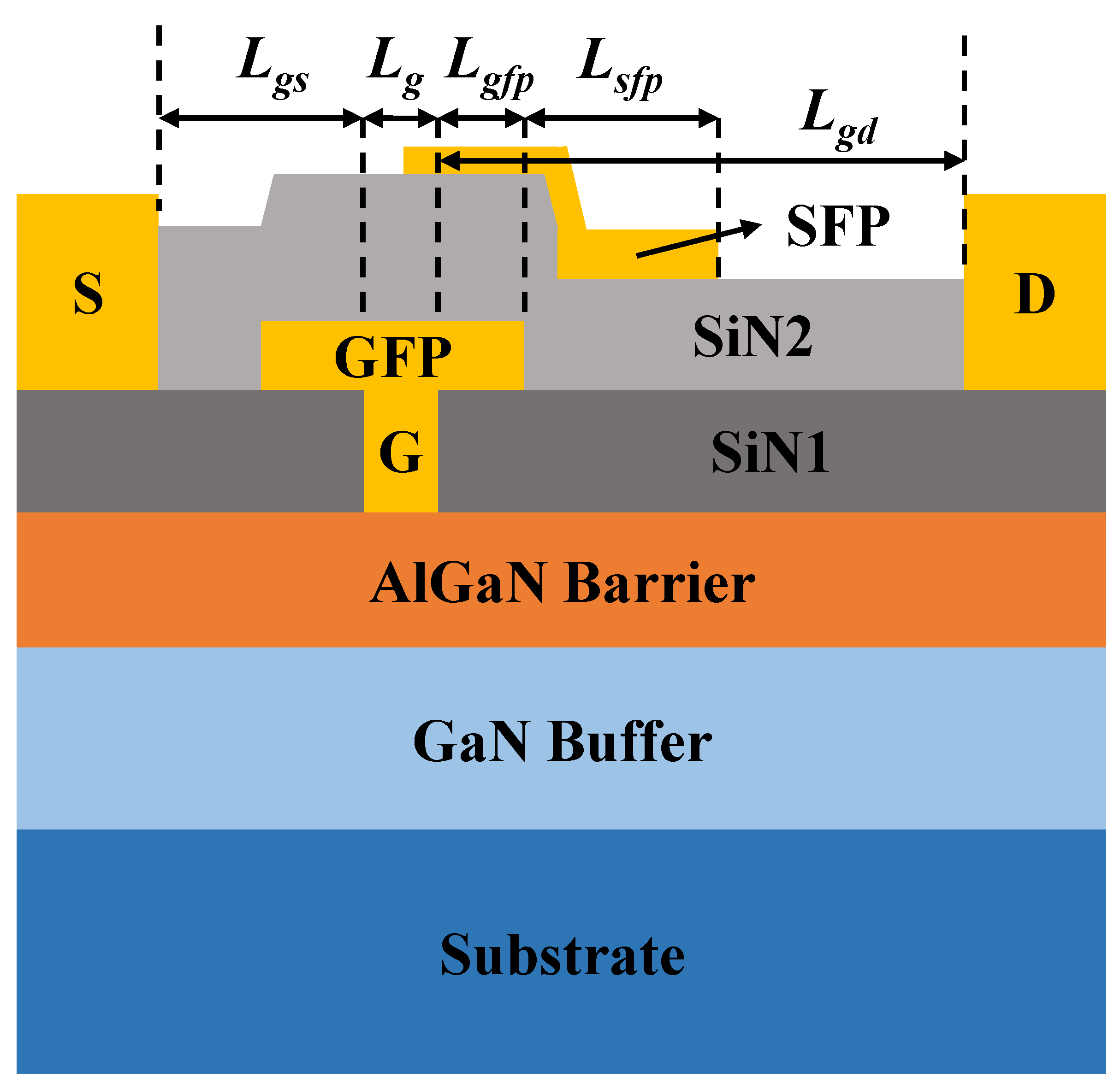
2.1. Novel Device Model
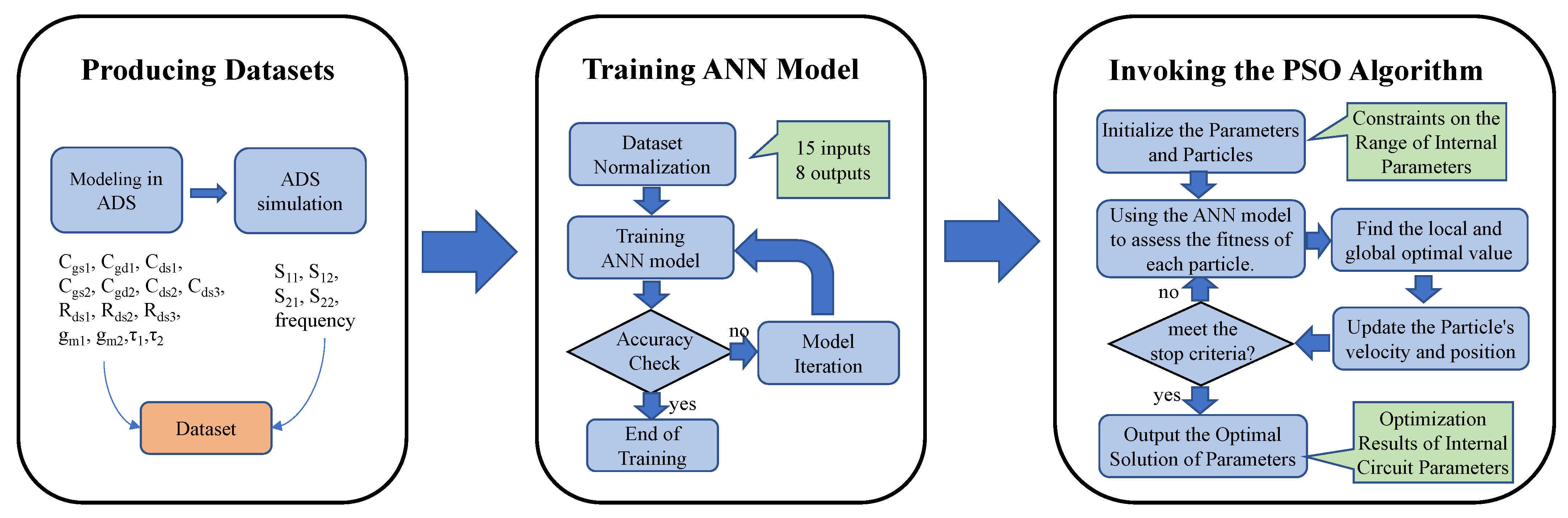
2.2. Model Optimization Method
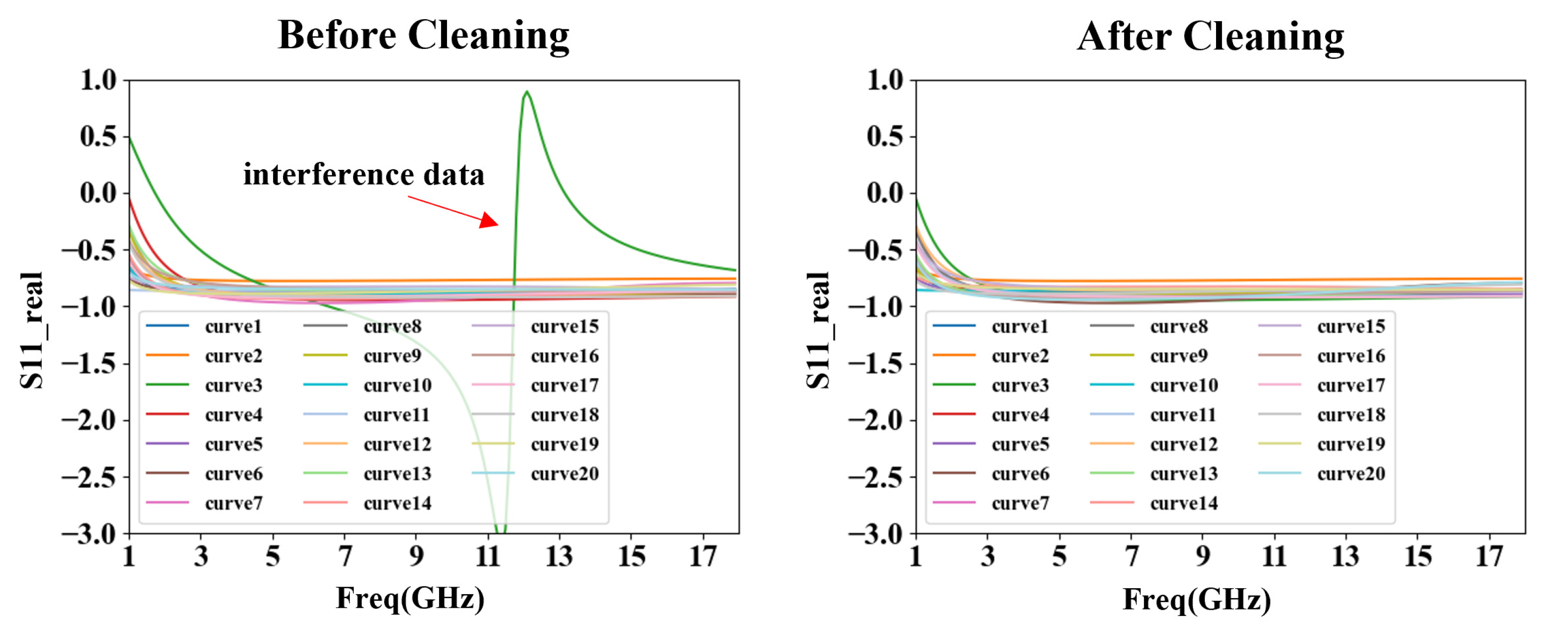
2.2.1. Producing Datasets
2.2.2. Training the ANN Model
2.2.3. Invoking the PSO Algorithm
3. Results
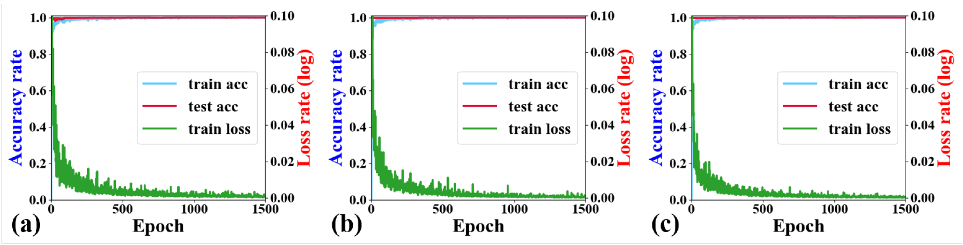
3.1. ANN Accuracy
3.2. Optimization Algorithm Comparison
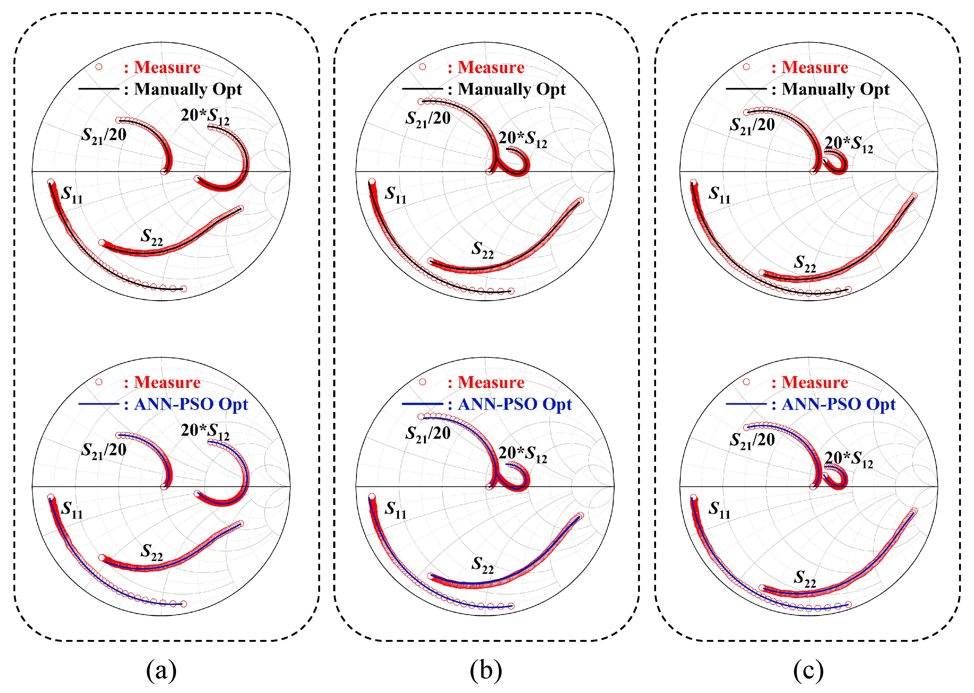
3.3. ANN-PSO Optimization Results
4. Discussion
5. Conclusions
Author Contributions
Funding
Data Availability Statement
Acknowledgments
Conflicts of Interest
References
- Ma, R.; Wang, Z.; Yang, X.; Lanfranco, S. Implementation of a current-mode class-S RF power amplifier with GaN HEMTs for LTE-Advanced. In Proceedings of the WAMICON 2012 IEEE Wireless & Microwave Technology Conference, Cocoa Beach, FL, USA, 15–17 April 2012; pp. 1–6. [Google Scholar]
- Ye, H.; Wu, C.; Venkatesan, N.; Wang, J.; Cao, Y.; Xie, A.; Beam, E.; Fay, P. Ferroelectric-gated GaN HEMTs for RF and mm-wave switch applications. In Proceedings of the 2022 International Symposium on VLSI Technology, Systems and Applications (VLSI-TSA), Hsinchu, Taiwan, 18–21 April 2022; pp. 1–2. [Google Scholar]
- Jarndal, A.; Hussein, A.; Crupi, G.; Caddemi, A. Reliable noise modeling of GaN HEMTs for designing low-noise amplifiers. Int. J. Numer. Model. Electron. Netw. Devices Fields 2020, 33, e2585. [Google Scholar] [CrossRef]
- He, J.; Cheng, W.C.; Wang, Q.; Cheng, K.; Yu, H.; Chai, Y. Recent advances in GaN-based power HEMT devices. Adv. Electron. Mater. 2021, 7, 2001045. [Google Scholar] [CrossRef]
- Berzoy, A.; Lashway, C.R.; Moradisizkoohi, H.; Mohammed, O.A. Breakdown voltage improvement and analysis of GaN HEMTs through field plate inclusion and substrate removal. In Proceedings of the 2017 IEEE 5th Workshop on Wide Bandgap Power Devices and Applications (WiPDA), Albuquerque, NM, USA, 30 October–1 November 2017; pp. 138–142. [Google Scholar]
- Ahsan, S.A.; Ghosh, S.; Sharma, K.; Dasgupta, A.; Khandelwal, S.; Chauhan, Y.S. Capacitance modeling in dual field-plate power GaN HEMT for accurate switching behavior. IEEE Trans. Electron Devices 2015, 63, 565–572. [Google Scholar] [CrossRef]
- Kellogg, K.; Khandelwal, S.; Craig, N.; Dunleavy, L. Improved charge modeling of field-plate enhanced algan/gan hemt devices using a physics based compact model. In Proceedings of the 2018 IEEE BiCMOS and Compound Semiconductor Integrated Circuits and Technology Symposium (BCICTS), San Diego, CA, USA, 15–17 October 2018; pp. 102–105. [Google Scholar]
- Bothe, K.M.; Ganguly, S.; Guo, J.; Liu, Y.; Niyonzima, A.; Tornblad, O.; Fisher, J.; Gajewski, D.A.; Sheppard, S.T.; Noori, B. Improved X-band performance and reliability of a GaN HEMT with sunken source connected field plate design. IEEE Electron Device Lett. 2022, 43, 354–357. [Google Scholar] [CrossRef]
- Bahat-Treidel, E.; Hilt, O.; Brunner, F.; Sidorov, V.; Würfl, J.; Tränkle, G. AlGaN/GaN/AlGaN DH-HEMTs breakdown voltage enhancement using multiple grating field plates (MGFPs). IEEE Trans. Electron Devices 2010, 57, 1208–1216. [Google Scholar] [CrossRef]
- Wu, H.; Fu, X.; Hu, S. A 650 V Enhancement Mode GaN HEMT Device with Field Plate for Power Electronic Applications. In Proceedings of the 2021 International Conference on Electrical, Communication, and Computer Engineering (ICECCE), Kuala Lumpur, Malaysia, 12–13 June 2021; pp. 1–5. [Google Scholar]
- Godfrey, D.; Nirmal, D.; Arivazhagan, L.; Roy, B.; Chen, Y.L.; Yu, T.H.; Yeh, W.K.; Godwinraj, D. Investigation of AlGaN/GaN HEMT Breakdown analysis with Source field plate length for High power applications. In Proceedings of the 2020 5th International Conference on Devices, Circuits and Systems (ICDCS), Coimbatore, India, 5–6 March 2020; pp. 244–246. [Google Scholar]
- Chanchal, C.; Visvkarma, A.K.; Malik, A.; Laishram, R.; Rawal, D.; Saxena, M. Dependence of Gate Leakage Current on Efficacy of Gate Field Plate in AlGaN/GaN HEMT. In Proceedings of the 2022 IEEE VLSI Device Circuit and System (VLSI DCS), Kolkata, India, 26–27 February 2022; pp. 265–268. [Google Scholar]
- Hasan, M.T.; Asano, T.; Tokuda, H.; Kuzuhara, M. Current collapse suppression by gate field-plate in AlGaN/GaN HEMTs. IEEE Electron Device Lett. 2013, 34, 1379–1381. [Google Scholar] [CrossRef]
- Neha; Kumari, V.; Gupta, M.; Saxena, M. Breakdown Voltage Analysis of Different Field Plate AlGaN/GaN HEMTs: TCAD based Assessment. In Proceedings of the 2018 IEEE Electron Devices Kolkata Conference (EDKCON), Kolkata, India, 24–25 November 2018; pp. 407–412. [Google Scholar]
- Hu, Q.; Zeng, F.; Cheng, W.C.; Zhou, G.; Wang, Q.; Yu, H. Reducing dynamic on-resistance of p-GaN gate HEMTs using dual field plate configurations. In Proceedings of the 2020 IEEE International Symposium on the Physical and Failure Analysis of Integrated Circuits (IPFA), Singapore, 20–23 July 2020; pp. 1–4. [Google Scholar]
- Wen, Z.; Xu, Y.; Wang, C.; Zhao, X.; Xu, R. An efficient parameter extraction method for GaN HEMT small-signal equivalent circuit model. Int. J. Numer. Model. Electron. Netw. Devices Fields 2017, 30, e2127. [Google Scholar] [CrossRef]
- Khandelwal, S.; Chauhan, Y.S.; Hodges, J.; Albahrani, S.A. Non-linear rf modeling of gan hemts with industry standard asm gan model. In Proceedings of the 2018 IEEE BiCMOS and Compound Semiconductor Integrated Circuits and Technology Symposium (BCICTS), San Diego, CA, USA, 15–17 October 2018; pp. 93–97. [Google Scholar]
- Jarndal, A.; Kompa, G. A new small-signal modeling approach applied to GaN devices. IEEE Trans. Microw. Theory Tech. 2005, 53, 3440–3448. [Google Scholar] [CrossRef]
- Hodges, J.; Albahrani, S.A.; Khandelwal, S. A computationally efficient modelling methodology for field-plates in gan hemts. In Proceedings of the 2019 IEEE BiCMOS and Compound semiconductor Integrated Circuits and Technology Symposium (BCICTS), Nashville, TN, USA, 3–6 November 2019; pp. 1–4. [Google Scholar]
- Menokey, A.; Ajoy, A. Analytical model for off-state channel potential and electric field distribution in an N-polar GaN-based field-plated MIS-HEMT. In Proceedings of the 2022 IEEE International Conference on Emerging Electronics (ICEE), Bangalore, India, 11–14 December 2022; pp. 1–5. [Google Scholar]
- Čučak, D.; Vasić, M.; García, O.; Oliver, J.A.; Alou, P.; Cobos, J.A.; Wang, A.; Martín-Horcajo, S.; Romero, M.F.; Calle, F. Physics-based analytical model for input, output, and reverse capacitance of a GaN HEMT with the field-plate structure. IEEE Trans. Power Electron. 2016, 32, 2189–2202. [Google Scholar] [CrossRef]
- Wang, J.; Liu, J.; Zhao, Z. A novel small-signal equivalent circuit model for GaN HEMTs incorporating a dual-field-plate. J. Semicond. 2024, 45, 052302. [Google Scholar] [CrossRef]
- Zhang, Q.J.; Gupta, K.C.; Devabhaktuni, V.K. Artificial neural networks for RF and microwave design-from theory to practice. IEEE Trans. Microw. Theory Tech. 2003, 51, 1339–1350. [Google Scholar] [CrossRef]
- Wang, Z.; Li, L.; Yao, Y. A machine learning-assisted model for GaN ohmic contacts regarding the fabrication processes. IEEE Trans. Electron Devices 2021, 68, 2212–2219. [Google Scholar] [CrossRef]
- Wang, Z.; Li, L.; Leon, R.C.; Yang, J.; Shi, J.; van der Laan, T.; Usman, M. Improving Semiconductor Device Modeling for Electronic Design Automation by Machine Learning Techniques. IEEE Trans. Electron Devices 2023, 71, 263–271. [Google Scholar] [CrossRef]
- Yee, N.; Lu, A.; Wang, Y.; Porter, M.; Zhang, Y.; Wong, H.Y. Rapid Inverse Design of GaN-on-GaN Diode with Guard Ring Termination for BV and (V F Q)- 1 Co-Optimization. In Proceedings of the 2023 35th International Symposium on Power Semiconductor Devices and ICs (ISPSD), Hong Kong, China, 28 May–1 June 2023; pp. 143–146. [Google Scholar]
- Wu, T.L.; Kutub, S.B. Machine learning-based statistical approach to analyze process dependencies on threshold voltage in recessed gate AlGaN/GaN MIS-HEMTs. IEEE Trans. Electron Devices 2020, 67, 5448–5453. [Google Scholar] [CrossRef]
- Liu, S.; Duan, X.; Wang, S.; Zhang, J.; Hao, Y. Optimization of dual field plate AlGaN/GaN HEMTs using artificial neural networks and particle swarm optimization algorithm. IEEE Trans. Device Mater. Reliab. 2023, 23, 204–210. [Google Scholar] [CrossRef]
- Abubakr, A.; Hassan, A.; Ragab, A.; Yacout, S.; Savaria, Y.; Sawan, M. High-temperature modeling of the IV characteristics of GaN150 HEMT using machine learning techniques. In Proceedings of the 2018 IEEE International Symposium on Circuits and Systems (ISCAS), Florence, Italy, 27–30 May 2018; pp. 1–5. [Google Scholar]
- Marinković, Z.; Crupi, G.; Caddemi, A.; Marković, V. On the neural approach for FET small-signal modelling up to 50 GHz. In Proceedings of the 10th Symposium on Neural Network Applications in Electrical Engineering, Belgrade, Serbia, 23–25 September 2010; pp. 89–92. [Google Scholar]
- Khusro, A.; Hashmi, M.S.; Ansari, A.Q.; Auyenur, M. A new and reliable decision tree based small-signal behavioral modeling of GaN HEMT. In Proceedings of the 2019 IEEE 62nd International Midwest Symposium on Circuits and Systems (MWSCAS), Dallas, TX, USA, 4–7 August 2019; pp. 303–306. [Google Scholar]
- Khusro, A.; Husain, S.; Hashmi, M.S.; Ansari, A.Q. Small signal behavioral modeling technique of GaN high electron mobility transistor using artificial neural network: An accurate, fast, and reliable approach. Int. J. RF Microw. Comput.-Aided Eng. 2020, 30, e22112. [Google Scholar] [CrossRef]
- Ryu, W.; Yim, M.J.; Ahn, S.; Lee, J.; Kim, W.; Paik, K.W.; Kim, J. High-frequency SPICE model of anisotropic conductive film flip-chip interconnections based on a genetic algorithm. IEEE Trans. Components Packag. Technol. 2000, 23, 542–545. [Google Scholar]
- Li, Y.; Cho, Y.Y. Parallel genetic algorithm for SPICE model parameter extraction. In Proceedings of the 20th IEEE International Parallel & Distributed Processing Symposium, Rhodes, Greece, 25–29 April 2006; p. 8. [Google Scholar]
- Li, R.; Li, D.; Du, H.; Hai, C.; Han, Z. SOI MOSFET model parameter extraction via a compound genetic algorithm. Bandaoti Xuebao (Chin. J. Semicond.) 2006, 27, 796–803. [Google Scholar]
- Wu, Y. Parallel hybrid evolutionary algorithm based on chaos-GA-PSO for SPICE model parameter extraction. In Proceedings of the 2009 IEEE International Conference on Intelligent Computing and Intelligent Systems, Shanghai, China, 20–22 November 2009; Volume 1, pp. 688–692. [Google Scholar]
- Rizzo, S.A.; Salerno, N.; Raciti, A.; Bazzano, G.; Raffa, A.; Veneziano, P. Parameters optimization of a behavioural SPICE model of an automotive grade SiC MOSFET using Particle Swarm Optimization algorithm. In Proceedings of the 2020 International Symposium on Power Electronics, Electrical Drives, Automation and Motion (SPEEDAM), Sorrento, Italy, 24–26 June 2020; pp. 381–386. [Google Scholar]
- Sarvaghad-Moghaddam, M.; Orouji, A.A.; Ramezani, Z.; Elhoseny, M.; Farouk, A.; Arun Kumar, N. Modelling the spice parameters of SOI MOSFET using a combinational algorithm. Clust. Comput. 2019, 22, 4683–4692. [Google Scholar] [CrossRef]
- White, P.M.; Healy, R.M. Improved equivalent circuit for determination of MESFET and HEMT parasitic capacitances from “Coldfet” measurements. IEEE Microw. Guid. Wave Lett. 1993, 3, 453–454. [Google Scholar] [CrossRef]
- Cai, H.; Zhang, J.; Liu, M.; Yang, S.; Wang, S.; Liu, B.; Zhang, J. Adaptive particle swarm optimization based hybrid small-signal modeling of GaN HEMT. Microelectron. J. 2023, 137, 105834. [Google Scholar] [CrossRef]
- He, Y.; Ma, W.J.; Zhang, J.P. The parameters selection of PSO algorithm influencing on performance of fault diagnosis. MATEC Web Conf. 2016, 63, 02019. [Google Scholar] [CrossRef]
- Price, K. Differential Evolution: A Practical Approach to Global Optimization; Springer Science & Business Media: Berlin/Heidelberg, Germany, 2006. [Google Scholar]
- Deb, K.; Pratap, A.; Agarwal, S.; Meyarivan, T. A fast and elitist multiobjective genetic algorithm: NSGA-II. IEEE Trans. Evol. Comput. 2002, 6, 182–197. [Google Scholar] [CrossRef]
- Majumdar, A.; Chatterjee, S.; Chatterjee, S.; Chaudhari, S.S.; Poddar, D.R. Optimization of intrinsic elements from small signal model of GaN HEMT by using PSO. In Proceedings of the 2015 IEEE Applied Electromagnetics Conference (AEMC), Guwahati, India, 18–21 December 2015; pp. 1–2. [Google Scholar]


| Intrinsic Element | LB | UB |
|---|---|---|
| (fF) | 500 | 2000 |
| (fF) | 200 | 400 |
| (fF) | 5 | 50 |
| (fF) | 200 | 700 |
| (fF) | 10 | 50 |
| (fF) | 1 | 30 |
| (fF) | 1 | 200 |
| (Ω) | 5 | 20 |
| (Ω) | 100 | 500 |
| (Ω) | 20 | 70 |
| (ms) | 100 | 400 |
| (ms) | 50 | 250 |
| (ps) | 3000 | 5500 |
| (ps) | 2500 | 5000 |
| Bias Condition | Train_Loss (MSE) | Train_Accuracy () | Test_Accuracy () |
|---|---|---|---|
| = 28 V, = 1 V | 0.006170 | 0.999919 | 0.999920 |
| = 40 V, = −1 V | 0.006420 | 0.999825 | 0.999823 |
| = 48 V, = −3 V | 0.005304 | 0.999917 | 0.999917 |
| Parameter | Manually Tuned | PSO-Optimized | Absolute Error * |
|---|---|---|---|
| Bias condition at = 28 V, = 1 V | |||
| (fF) | 950.9 | 960.7 | 9.8 |
| (fF) | 229.0 | 228.7 | 0.3 |
| (fF) | 46.39 | 52.4 | 6.01 |
| (fF) | 338.7 | 359.8 | 21.1 |
| (fF) | 35.40 | 40.74 | 15.34 |
| (fF) | 20.31 | 21.93 | 1.62 |
| (fF) | 134.5 | 131.4 | 3.1 |
| (Ω) | 16.01 | 12.18 | 3.83 |
| (Ω) | 133.8 | 156.34 | 22.54 |
| (Ω) | 50.01 | 49.52 | 0.49 |
| (ms) | 202.2 | 213.7 | 11.5 |
| (ms) | 110.8 | 115.2 | 4.4 |
| (ps) | 4.309 | 4.181 | 0.128 |
| (ps) | 3.677 | 3.901 | 0.244 |
| Bias condition at = 40 V, = −1 V | |||
| (fF) | 976.7 | 942.7 | 34.0 |
| (fF) | 294.8 | 270.2 | 24.6 |
| (fF) | 15.50 | 10.17 | 5.33 |
| (fF) | 660.2 | 414.4 | 245.8 |
| (fF) | 10.91 | 12.86 | 1.95 |
| (fF) | 13.66 | 11.05 | 2.61 |
| (fF) | 104.7 | 106.5 | 1.8 |
| (Ω) | 8.317 | 8.887 | 0.57 |
| (Ω) | 208.9 | 207.5 | 1.4 |
| (Ω) | 28.45 | 33.6 | 5.15 |
| (ms) | 288.0 | 288.4 | 0.4 |
| (ms) | 167.1 | 151.7 | 15.4 |
| (ps) | 4.307 | 4.160 | 0.147 |
| (ps) | 3.624 | 3.931 | 0.307 |
| Bias condition at = 48 V, = −3 V | |||
| (fF) | 913.1 | 898.6 | 14.5 |
| (fF) | 244.3 | 264.5 | 20.2 |
| (fF) | 9.731 | 8.761 | 0.97 |
| (fF) | 539.1 | 459.7 | 79.4 |
| (fF) | 13.13 | 12.94 | 0.19 |
| (fF) | 23.39 | 23.58 | 0.19 |
| (fF) | 60.77 | 62.03 | 1.26 |
| (Ω) | 6.449 | 6.784 | 0.335 |
| (Ω) | 351.8 | 340.1 | 11.7 |
| (Ω) | 44.1 | 45.4 | 1.3 |
| (ms) | 207.6 | 223.9 | 16.3 |
| (ms) | 179.3 | 164.3 | 15 |
| (ps) | 4.609 | 4.002 | 0.607 |
| (ps) | 3.881 | 3.892 | 0.011 |
| Bias Condition | Optimization Method | (%) | (%) | (%) | (%) | (%) |
|---|---|---|---|---|---|---|
| = 28 V | Manual | 1.549 | 3.192 | 6.872 | 2.393 | 3.5015 |
| = 1 V | ANN-PSO | 1.231 | 3.199 | 12.36 | 2.791 | 4.8953 |
| = 40 V | Manual | 1.176 | 4.797 | 4.072 | 2.173 | 3.0545 |
| = −1 V | ANN-PSO | 1.637 | 5.369 | 5.391 | 3.790 | 4.0468 |
| = 48 V | Manual | 1.314 | 9.284 | 4.511 | 2.576 | 4.4213 |
| = −3 V | ANN-PSO | 1.007 | 9.248 | 5.015 | 2.172 | 4.3605 |
Disclaimer/Publisher’s Note: The statements, opinions and data contained in all publications are solely those of the individual author(s) and contributor(s) and not of MDPI and/or the editor(s). MDPI and/or the editor(s) disclaim responsibility for any injury to people or property resulting from any ideas, methods, instructions or products referred to in the content. |
© 2024 by the authors. Licensee MDPI, Basel, Switzerland. This article is an open access article distributed under the terms and conditions of the Creative Commons Attribution (CC BY) license (https://creativecommons.org/licenses/by/4.0/).
Share and Cite
Shen, H.; Zhou, W.; Wang, J.; Jin, H.; Wu, Y.; Wang, J.; Liu, J. A Novel ANN-PSO Method for Optimizing a Small-Signal Equivalent Model of a Dual-Field-Plate GaN HEMT. Micromachines 2024, 15, 1437. https://doi.org/10.3390/mi15121437
Shen H, Zhou W, Wang J, Jin H, Wu Y, Wang J, Liu J. A Novel ANN-PSO Method for Optimizing a Small-Signal Equivalent Model of a Dual-Field-Plate GaN HEMT. Micromachines. 2024; 15(12):1437. https://doi.org/10.3390/mi15121437
Chicago/Turabian StyleShen, Haowen, Wenyong Zhou, Jinye Wang, Hangjiang Jin, Yifan Wu, Junchao Wang, and Jun Liu. 2024. "A Novel ANN-PSO Method for Optimizing a Small-Signal Equivalent Model of a Dual-Field-Plate GaN HEMT" Micromachines 15, no. 12: 1437. https://doi.org/10.3390/mi15121437
APA StyleShen, H., Zhou, W., Wang, J., Jin, H., Wu, Y., Wang, J., & Liu, J. (2024). A Novel ANN-PSO Method for Optimizing a Small-Signal Equivalent Model of a Dual-Field-Plate GaN HEMT. Micromachines, 15(12), 1437. https://doi.org/10.3390/mi15121437