1. Introduction
Coplanar interdigitated finger electrodes can be used for a di-electrowetting system [
1,
2,
3,
4,
5,
6]. The design of electrodes was different with conventional solid square or rectangle shapes for EWOD (electrowetting-on-dielectric) system. Although the behavior in the contact angle change in the di-electrowetting system is apparently similar to EWOD system [
7,
8,
9,
10], its physics and mechanism are quite different.
MacHale’s team introduced a di-electrowetting concept that is based on liquid di-electrophoresis (L-DEP) [
11,
12,
13]. They used coplanar interdigitated finger electrodes for distinguishing di-electrowetting. Identically, Jones’s also introduced a similar concept through L-DEP for microfluidics application [
14,
15,
16,
17,
18,
19,
20,
21,
22,
23]. The driving force of di-electrowetting is the liquid dielectrophoretic force that is generated from charge diploes induced by a non-homogeneous electric field. Two adjacent electrode fingers will be generated by non-homogeneous fringe fields when a voltage is applied.
Brown’ s team [
24,
25,
26] demonstrated a periodic wrinkle that is formed by dielectrophoretic actuation. The thickness of the liquid was very thin and was less than the penetration depth. This means that the fringe electric field would affect the top liquid–vapor interface.
In 2009, Fair et al. proposed a scale model of a dielectric wetting actuator [
27]. By considering contact-angle hysteresis, the resistance of the upper and lower plates and the change in force when driving a droplet to move between the electrodes, the minimum voltage value to drive the droplet was calculated, which was related to the electrode width, the thickness of the dielectric layer, and the distance between the upper and lower plates, which were proportional to the ratio. When the electrode size decreased, the distance moved by a droplet generated by the storage tank thus also decreased, which was helpful for the generation of microdroplets.
In 2013, Hiroyuki Fujita’s team proposed a method to fabricate microfluidic wafers rapidly using dielectric-wetted array wafers [
28]. This method injected liquid paraffin into the wafer instead of air as the medium during the first step, then injected deionized water into the array wafer. The final step was to turn on a specific electrode and apply a voltage 50~150 Vrms/50 kHz to drive the liquid beads so as to form the desired pattern. After the pattern was formed, the AC (alternating current) signal was maintained on the selected electrodes so as to maintain the shape of the DI (deionized water) water. The wafer temperature was lowered by thermoelectric cooling of the wafer; the temperature was in the range of +45 °C to −40 °C. The entire solidification took 5 s to complete. With this wafer for microfluidic patterning, by programming the change in wafer temperature, the transition from English letter “C” to “A” could be completed in less than 5 min.
In 2015, Papautsky et al. proposed combining continuous microfluidics and digital microfluidics into a microfluidic platform that could be programmed [
29]. This study was helpful for the application of microfluidics and biomedical clinical diagnosis. The chip was composed of programmable two-dimensional array electrodes on the bottom plate, with 5 × 8 electrodes in total; the electrode size was 1 mm × 1 mm, the upper cover and the bottom plate were separated by 100 μm, and a syringe pump was used to inject liquid at the inlet. The same amount of liquid was injected from the inlet into six of the nine cell array electrodes in the wafer; the electrodes were turned on with the letter “U”; after two seconds, the letter “C” formed, and then the letter “T” formed. Finally, the letter “U” formed.
The main purpose of this study is to manipulate UV resin for patterning through dielectric force. UV resin is an adhesive material that can be solidified through exposure to UV light, and it is commonly used a glue for paint, coating, and ink. We also discuss the influence of electric field conditions on UV resin manipulation. Finally, through the dielectric force applied on the UV resin, the patterned arrangement of UV resin is further manipulated. After we patterned the UV resin, applied with UV light, we successfully demonstrated the fabrication of tiny structures.
2. Theory and Experimental Setup
2.1. Theory of Dielectric Force
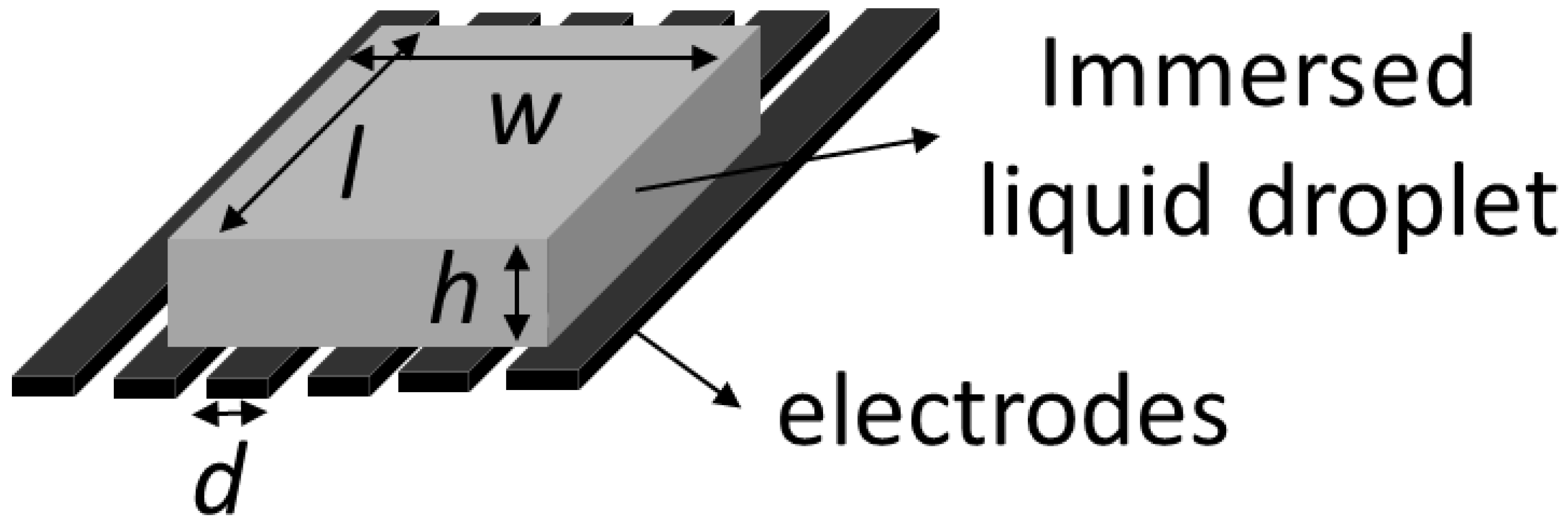
If droplets are immersed in the other immiscible dielectric liquid with a low dielectric constant, this phenomenon is called di-electrowetting. The elongation of a droplet could be calculated by the following equation [
30]:
where
is the height of the droplet and
is the initial height of the droplet, while
= 0 V,
Ω =
hl,
l is the contact length of the droplet in elongation.
δ is the penetration depth of the electric field (=4 ω/π).
is the interfacial tension between the droplet liquid and immersion fluid.
is the amplitude of applied voltage to the electrodes.
,
, and
are the permittivities of the droplet liquid, surround fluid and free space, respectively. The thickness of the droplet is proportional to the square of
and the ratio of difference in permittivity to the liquid–fluid interfacial tension (
. The dielectric model was shown in
Figure 1 [
30].
2.2. Dielectric Chip Manipulate System
The experimental setup of this research (shown in
Figure 2) included a dielectric chip holding platform, a UV-curing module (UV mercury lamp (350–450 nm)), a CCD (Charge-coupled Device) alignment system (Confocal Displacement Sensor, CL 3000, KEYENCE), a signal generator (33220A, Keysight), a power amplifier (A304, A. A. Lab system Ltd., Wilmington, DE, USA), a microscope observation module, load/unload platform, and a vacuum module. The designed dielectric chip was placed on the platform and was connected to the relay. The relay could correspond to 160 sets of independent electrode switches, and the patterned control electrode could drive the UV resin.
After the UV resin was driven by the AC electrical field, the UV and vacuum module picked up the glass substrate through the x-y motion platform with ±0.01 mm repeatability (R138, Yu-Zhan motion technology, Taichung City, Taiwan). The vacuum module was moved to just above the dielectric chip, and was in contact with the patterned UV resin. Then, the UV light was turned on for curing to complete the formation of the first layer structure. This procedure is shown in
Figure 2b.
2.3. UV-Curable Resin
This research used UV-SIL photosensitive polymer material (Agent company in Taiwan was Heart-bond industrial materials LTD., the manufacturer was Adhetron in USA.) mixed with propylene carbonated (CAS number: 108-32-7) as a dielectric force driving liquid.
UV SIL is a is non-corrosive, single-component silicone elastomer material that will cure to a soft rubber after exposure to UV light [
31]. The mixing ratio was 80% UV SIL and 20% propylene carbonate. The main purpose for choosing PC (propylene carbonate) was to ensure the driving liquid would have a good permittivity with 66.1 Tm/A (permittivity), which is in excellent agreement Equation 1. UV resin composed of UV-SIL and propylene carbonate is a kind of adhesive material that is cured with UV light (absorption wavelength was 365 nm) and can be used as a glue for paints, coatings, inks, etc. The principle of UV resin curing is that the photo-initiator (or photosensitizer) in the UV curing material generates active free radicals or cations after absorbing ultraviolet light, which initiates monomer polymerization, cross-linking, and branching chemical reactions. The adhesive changes from liquid to solid within a few seconds. The scheme of reaction of UV resin after UV exposure is shown in
Figure 3.
2.4. Dielectric Chip Design and Manufacture
The metal-electrode structure was formed through photolithography on a silicon wafer [
32]. Spin coating was used to deposit a dielectric insulation layer (the insulating layer material can be silicon nitride, SU8 photoresist, etc.) and hydrophobic layer (the hydrophobic layer material can be Teflon, Cytop, etc.). The manufacture flow is shown in
Figure 4a.
As the hydrophobic layer plays an important role in resin patterning, when a dielectric chip is made, the hydrophobic characteristics must be analyzed first and the contact angle must be larger than 90°.
We used an 8-inch silicon substrate to make electrodes for the dielectric chip (shown in
Figure 4b), with four sets of electrodes in this 8-inch silicon substrate. The electrode size of each set was 1.2 mm × 1.2 mm, 2.0 mm × 2.0 mm, 2.6 mm × 2.6 mm, 4.6 mm × 4.6 mm. In addition, the interdigital electrode applied in the dielectric chip increased the driving force of the resin, making it easier to move and to control the UV resin.
Figure 4c shows that the line width and line distance of each interdigital electrode were 10 µm and 10 µm.
3. Results and Discussion
3.1. Influence of Current and Voltage on UV Resin Drive by Dielectric Force
The voltage change was set from 100 V to 300 V, at intervals of 50 V. In addition, current conditions are set for each voltage condition, ranging from 0.1 A to 0.5 A. The frequency of the AC electric field was fixed at 40 kHz. The sample volume was controlled at
As
Figure 5 shows, the sample was stretched to a square pattern by four electrodes switched at the same time. The measurement result of the square area was considered as the influence of voltage and current. When the current condition was fixed and the voltage change increased from 100 V to 300 V, the shape of the droplet expanded to a specific area. This means that the voltage increased by 300%, while the shape of the droplet increased by 200%, as shown in
Figure 6. Observing the trend of the results shows that the sample stretch was affected by the electric current condition.
Under the fixed voltage condition, the current increased from 0.1 A to 0.5 A. As shown in
Figure 7, taking the voltage condition of 150 V as an example, the current increased by 500%, and the shape of the droplet increased by 180%. The resulting trends for changing the current under different specific voltage conditions were similar. According to the data observation, the voltage had a positive exponential relationship with the area.
The final paragraphs provide the pattern result for different driving voltages and currents. We discovered the relationship for the condition of a fixed current. The area of the droplet expanded by 28% for every 10 V increase in voltage before the droplet expanded in the saturation area. On the contrary, under the condition of fixed voltage, the area of droplet expanded by 1 mm2 for every 0.1 A increase in current. Based on the above results, in addition to the voltage affecting the area of the droplet, the current also played an important role.
3.2. Influence of Electric Field Frequency on the Linewidth after UV Resin Drive
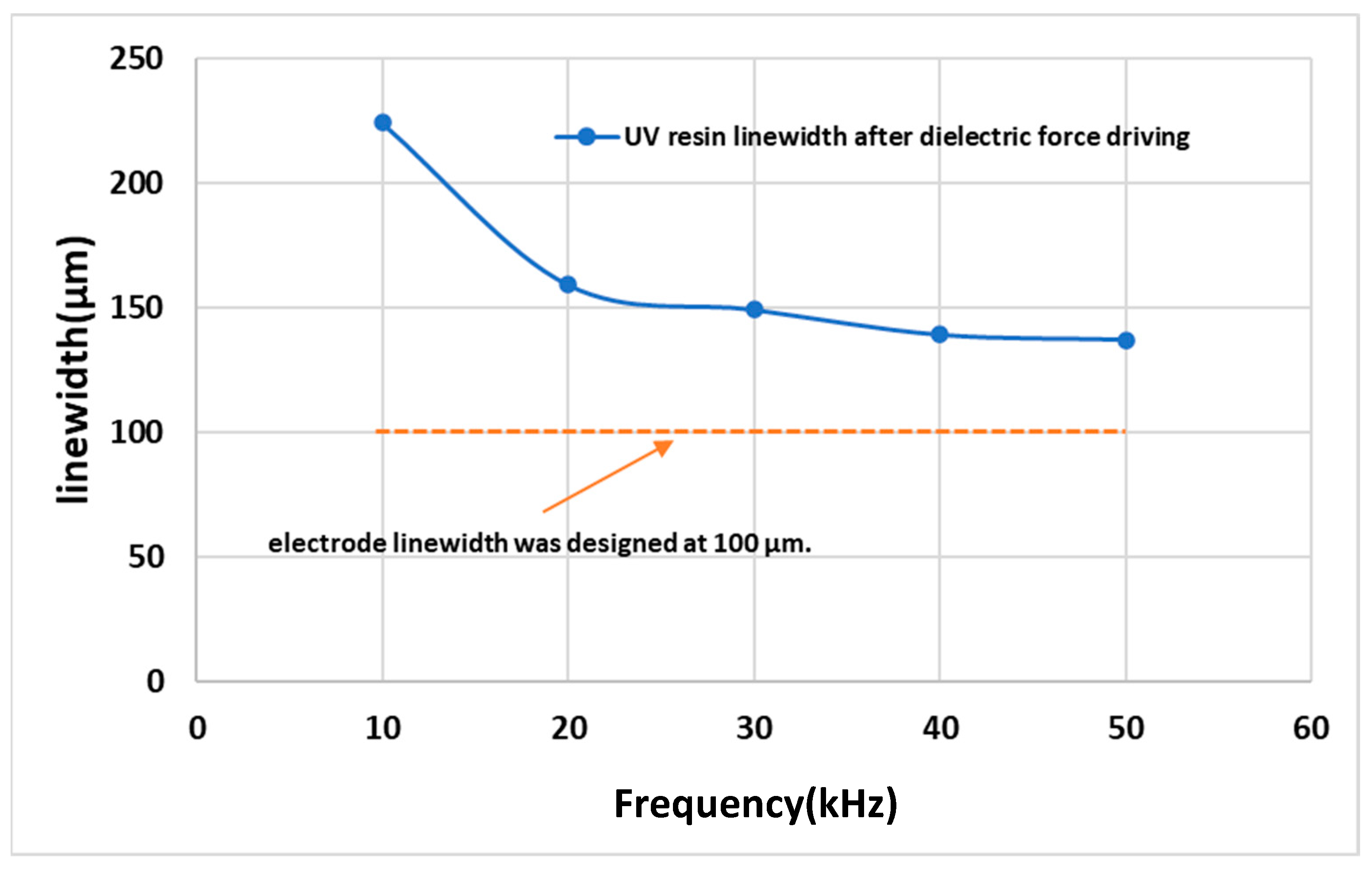
Through control of the electric field, the charge distribution on the surface of the colloid could be further varied. The UV resin could achieve the purpose of patterning. In addition to the voltage and current that can affect the driving of the UV resin, we found that the frequency adjustment of the alternating current could affect the appearance of the line width after the UV resin was driven. This section discusses the relationship between the frequency of the electric field and line width after UV resin was driven. The voltage condition of the test was fixed at 200 Vcc and the current was fixed at 0.3 A. The frequency was adjusted from 10 kHz to 50 kHz at intervals of 10 kHz. The test results in
Figure 8a show that when the frequency condition was 10 kHz, the UV resin could be formed along the electrode, but the edge of the UV resin was jagged and could not form a straight line. The line width of the UV resin after driving was larger than the line width of the electrode itself, reaching 224 μm. To make the UV resin after driving appear straight and further decrease the line width, we increased the frequency. The results in
Figure 8a–e show that the line edge and line width after UV resin driving could become straighter and the line width became smaller as the frequency increased. When the electric field frequency increased from 10 kHz to 20 kHz, the line edge and line width were obviously different. The minimum line width could reach 137 μm, which was close to the electrode linewidth of 100 μm.
As shown in
Figure 9, when the frequency increased from 10 kHz to 50 kHz, the line width of the UV resin after being driven by dielectric force was significantly reduced from 224 μm to 137 μm. The line width of the electrode design was 100 μm, and the difference was reduced from 124 μm to 37 μm. From the results, we can see that under the same voltage and current conditions, increasing the frequency could effectively reduce the line width of the UV resin after dielectric force was applied. This could improve the driving precision of the UV resin.
Through the dielectric system, this study successfully demonstrated that the patterning of UV resin could be performed using electrode control. Curing through UV light and repeated patterning and curing steps produced tiny structural parts of different shapes. As shown in
Figure 10, a structure with a thickness of about 1~2 mm could be formed by dielectric force and cured by UV light.
The results of this study were compared with conventional 3D printing techniques, as shown in
Table 1. The main difference was that the fabrication of structural electronics could be carried out through the same system in this study. There was an opportunity to create conductive layers inside the structure. In addition, the performance of fineness could be optimized by designing the size of the electrodes and the frequency of the applied electric field. The fineness could reach a micron level. In the future, there will be opportunities to apply structural electronic verification in the RD stage, which can accelerate the time course of product development.
4. Conclusions
Dielectric force-drivable UV resin, a dielectric chip, and manipulation equipment were developed in this study. We proposed a control model for the current and voltage of the electric field that drives the UV resin effectively. Current played an essential role in the dielectric system. The system provided a pattern instant curing ability with UV treatment.
Through the pattern curing experiment results, the appearance, area, and length of UV resin were affected by the applied current, voltage, and frequency on the dielectric chip. Therefore, the manipulation of dielectric force could be used as a reference for subsequent applications in the fabrication of tiny structures.
We found that current could significantly control the area of the droplet compared with the voltage. A phenomenon was found, where under a voltage fixed to 150 V, the droplet area was expended from 4.7 mm2 to 8.4 mm2 with an input current of 0.1 A to 0.5 A. While the current was set to 0.3 A, the droplet area expended within 5.6 mm2 to 6.5 mm2 with an input voltage of 100 V to 300 V. The test results indicate that the droplet was mainly affected by the current strength of the electric field. We further increased the morphological feature fining by a factor. Through the different frequency conditions, a coarse and fining pattern edge result was displayed. The line edge was relatively straight. The minimum line width attained was 137 μm.
An embedded conductive circuit inside the structure was accomplished through the integration of a mature inkjet printing technology in this system. According to the report by the Global Structural Electronics Market [
33], the market will be raising CAGR by 23.8% based on USD 1.5 billion in 2021 to 2030. Automotive, aerospace, and other electronics industries are different application fields for structure electronics. A hybrid system is necessary for the development of structure electronics technology. Therefore, this research has great potential to be integrated with maskless printing technology and to be applied to structure electronics. In the future, there will be opportunities to apply structural electronic verification in the RD stage, which can accelerate the time course of product development.
Author Contributions
Conceptualization and methodology, Y.-W.L. and D.-J.Y.; investigation and data curation, C.-Y.C., Y.-F.C., Y.-N.C. and D.-J.Y.; project administration and funding acquisition, D.-J.Y. All authors have read and agreed to the published version of the manuscript.
Funding
Financial support was provided from the R&D Program (Program Number: J301AR3D20) of ITRI (Industrial Technology Research Institute), Taiwan. We express gratitude for the smooth progress of this project.
Data Availability Statement
The data presented in this study are available upon request from the corresponding author.
Conflicts of Interest
The authors declare no conflict of interest.
References
- Xu, S.; Ren, H.W.; Wu, S.T. Dielectrophoretically tunable optofluidic devices. J. Phys. D Appl. Phys. 2013, 46, 483001–483014. [Google Scholar] [CrossRef]
- Zhao, R.; Cumby, B.; Russell, A.; Heikenfeld, J. Large area and low power dielectrowetting optical shutter with local deterministic fluid film breakup. Appl. Phys. Lett. 2013, 103, 223510–223514. [Google Scholar] [CrossRef]
- Russell, A.; Kreit, E.; Heikenfeld, J. Scaling dielectrowetting optical shutters to higher resolution: Microfluidic and optical implications. Langmuir 2014, 30, 5357–5362. [Google Scholar] [CrossRef] [PubMed]
- Russell, A.C.; Hsieh, W.L.; Chen, K.C.; Heikenfeld, J. Experimental and numerical insights into isotropic spreading and deterministic dewetting of dielectrowetted films. Langmuir 2015, 31, 637–642. [Google Scholar] [CrossRef] [PubMed]
- Brabcova, Z.; McHale, G.; Wells, G.G.; Brown, C.V.; Newton, M.I.; Edwards, A.M. Near axisymmetric partial wetting using interface-localized liquid dielectrophoresis. Langmuir 2016, 32, 10844–10850. [Google Scholar] [CrossRef]
- Geng, H.; Cho, S.K. Dielectrowetting for digital microfluidics. In Advances in Contact Angle, Wettability and Adhesion; Mittal, K.L., Ed.; Wiley-Scrivener: Beverly, MA, USA, 2018; Volume 3. [Google Scholar]
- Nelson, W.C.; Kim, C.J. Droplet actuation by electrowetting-on-dielectric (EWOD): A review. J. Adhesion Sci. Technol. 2012, 26, 1747–1771. [Google Scholar] [CrossRef]
- Cho, S.K.; Moon, H. Electrowetting on dielectric (EWOD): New tool for bio/micro fluid handling. BioChip J. 2008, 2, 79–96. [Google Scholar]
- Jones, T.B.; Wang, K.L.; Yao, D.J. Frequency-dependent electromechanics of aqueous liquids: Electrowetting and dielectrophoresis. Langmuir 2004, 20, 2813–2818. [Google Scholar] [CrossRef]
- Yoon, M.G.; Byun, S.H.; Cho, S.K. Inherent amplitude demodulation of an AC-EWOD (electrowetting on dielectric) droplet. Lab Chip 2013, 13, 662–668. [Google Scholar] [CrossRef]
- McHale, G.; Brown, C.V.; Newton, M.I.; Wells, G.G.; Sampara, N. Dielectrowetting driven spreading of droplets. Phys. Rev. Lett. 2011, 107, 186101–186104. [Google Scholar] [CrossRef]
- McHale, G.; Brown, C.V.; Newton, M.I.; Wells, G.G.; Sampara, N. Developing interface localized liquid dielectrophoresis for optical applications. In Proceedings of the Optical Design and Testing V, Beijing, China, 5–7 November 2012; Volume 855703. [Google Scholar]
- McHale, G.; Brown, C.V.; Sampara, N. Voltage-induced spreading and superspreading of liquids. Nature Commun. 2013, 4, 2619–2625. [Google Scholar] [CrossRef]
- Jones, T.B. Liquid dielectrophoresis on the microscale. J. Electrost. 2001, 51, 290–299. [Google Scholar] [CrossRef]
- Srinivasan, V.; Pamula, V.K.; Fair, R.B. An integrated digital microfluidic lab-on-achip for clinical diagnostics on human physiological fluids. Lab Chip 2004, 4, 310–315. [Google Scholar] [CrossRef] [PubMed]
- Abgrall, P.; Gue, A. Lab-on-chip technologies: Making a microfluidic network and coupling it into a complete microsystem—A review. J. Micromech. Microeng. 2007, 17, 15–49. [Google Scholar] [CrossRef]
- Dittrich, P.S.; Manz, A. Lab-on-a-chip: Microfluidics in drug discovery. Nat. Rev. Drug Discov. 2006, 5, 210–218. [Google Scholar] [CrossRef]
- Haeberle, S.; Zengerle, R. Microfluidic platforms for lab-on-a-chip applications. Lab Chip 2007, 7, 1094–1110. [Google Scholar] [CrossRef]
- Fair, R.B. Digital microfluidics: Is a true lab-on-a-chip possible? Microfluid. Nanofluid. 2007, 3, 245–281. [Google Scholar] [CrossRef]
- Choi, K.; Ng, A.H.C.; Fobel, R.; Wheeler, A.R. Digital microfluidics. Annu. Rev. Anal. Chem. 2012, 5, 413–440. [Google Scholar] [CrossRef]
- Beni, G.; Hackwood, S. Electro-wetting displays. Appl. Phys. Lett. 1981, 38, 207–209. [Google Scholar] [CrossRef]
- Berge, B.; Peseux, J. Variable focal lens controlled by an external voltage: An application of electrowetting. Eur. Phys. J. E 2000, 3, 159–163. [Google Scholar] [CrossRef]
- Pollack, M.G.; Fair, R.B.; Shenderov, A.D. Electrowetting-based actuation of liquid droplets for microfluidic applications. Appl. Phys. Lett. 2000, 77, 1725–1726. [Google Scholar] [CrossRef]
- Brown, C.V.; Wells, G.G.; Newton, M.I.; McHale, G. Voltage-programmable liquid optical interface. Nat. Photonics 2009, 3, 403–405. [Google Scholar] [CrossRef]
- Brown, C.V.; Al-Shabib, W.; Wells, G.G.; McHale, G.; Newton, M.I. Amplitude scaling of a static wrinkle at an oil-air interface created by dielectrophoresis forces. Appl. Phys. Lett. 2010, 97, 242904–242907. [Google Scholar] [CrossRef]
- Brown, C.V.; McHale, G.; Mottram, N.J. Analysis of a static undulation on the surface of a thin dielectric liquid layer formed by dielectrophoresis forces. J. Appl. Phys. 2011, 110, 024107–024112. [Google Scholar] [CrossRef]
- Song, J.; Evans, R.; Lin, Y.-Y.; Hsu, B.-N.; Fair, R.B. A scaling model for electrowetting-on-dielectric microfluidic actuators. Microfluid. Nanofluid. 2009, 7, 75–89. [Google Scholar] [CrossRef]
- Renaudot, R.; Agache, V.; Fouillet, Y.; Laffite, G.; Bisceglia, E.; Jalabert, L.; Kumemura, M.; Collard, D.; Fujita, H. A programmable and reconfigurable microfluidic chip. Lab Chip 2013, 13, 4517–4524. [Google Scholar] [CrossRef]
- Banerjee, A.; Noh, J.H.; Liu, Y.; Rack, P.D.; Papautsky, I. Programmable electrowetting with channels and droplets. Micromachines 2015, 6, 172–185. [Google Scholar] [CrossRef]
- Brown, C.V.; McHale, G.; Trabi, C.L. Dielectrophoresis-driven spreading of immersed liquid droplets. Langmuir 2015, 31, 1011–1016. [Google Scholar] [CrossRef]
- Adhetron. Available online: https://adhetron.com/uv-sil-3011/ (accessed on 2 February 2023).
- Lin, Y.-W.; Ciou, Y.-J.; Yao, D.-J. Virtual Stencil for Patterning and Modeling in a Quantitative Volume Using EWOD and DEP Devices for Microfluidics. Micromachines 2021, 12, 1104. [Google Scholar] [CrossRef]
- Global Structural Electronics Market by Type (Printed and Flexible Electronics, 3D Printers, Origami Zippered Tubes, Others), by Application (Aerospace, Automotive, Electricity, Others) and by Region (North America, Latin America, Europe, Asia Pacific and Middle East & Africa), Forecast from 2022 to 2030. Market Research Report, Report ID: 80725. 2022. Available online: https://dataintelo.com/report/structural-electronics-market/. (accessed on 19 February 2023).
| Disclaimer/Publisher’s Note: The statements, opinions and data contained in all publications are solely those of the individual author(s) and contributor(s) and not of MDPI and/or the editor(s). MDPI and/or the editor(s) disclaim responsibility for any injury to people or property resulting from any ideas, methods, instructions or products referred to in the content. |
© 2023 by the authors. Licensee MDPI, Basel, Switzerland. This article is an open access article distributed under the terms and conditions of the Creative Commons Attribution (CC BY) license (https://creativecommons.org/licenses/by/4.0/).


