
High Step-Up Ratio DC-AC Converter Using Fourth-Order LCLC Resonant Circuit for Ultrasonic Fingerprint-Sensor Drivers


Abstract
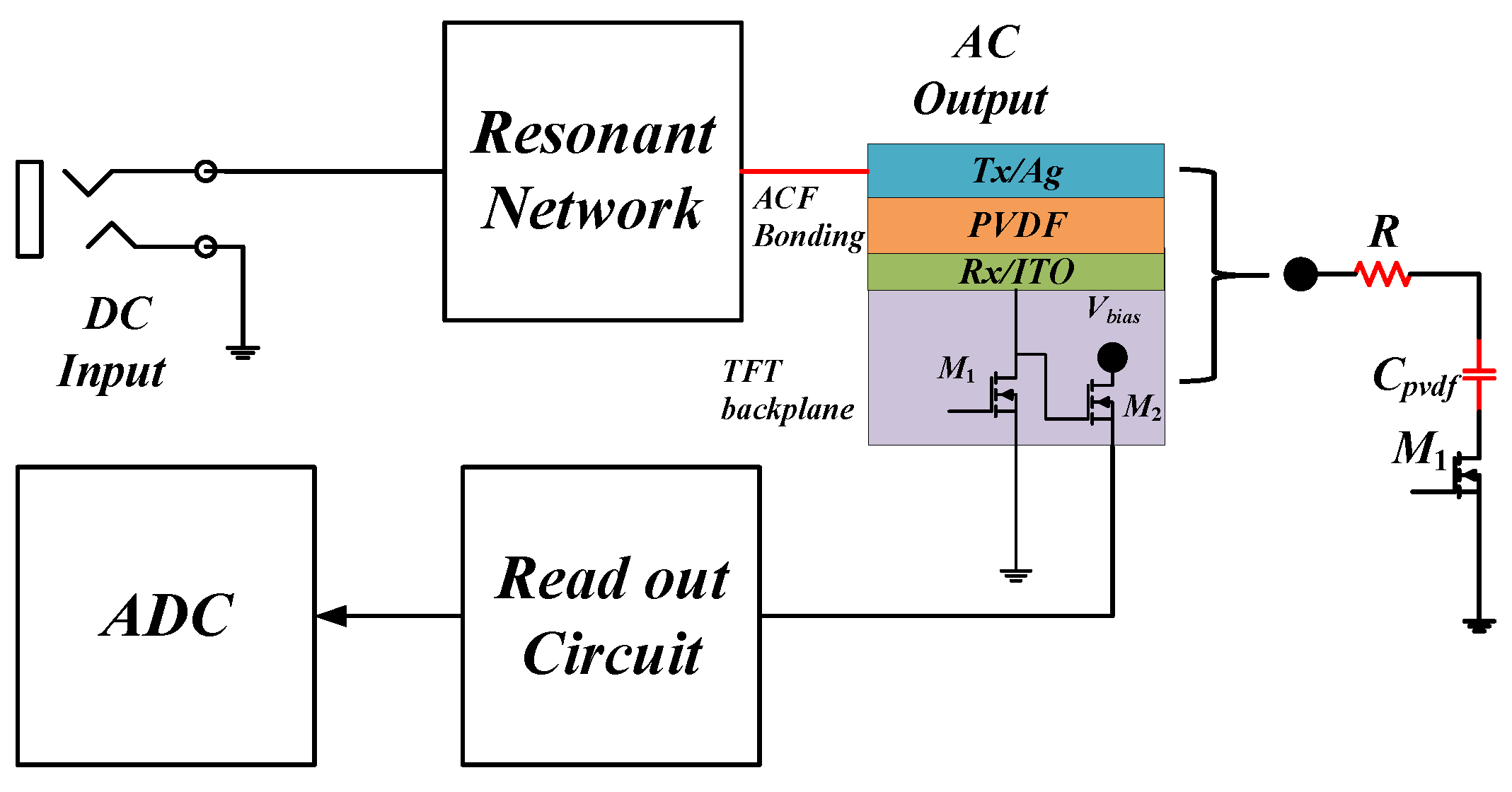
:1. Introduction
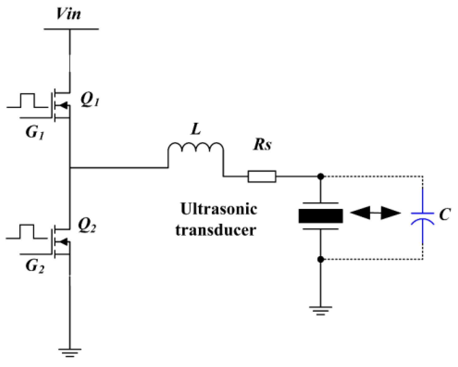
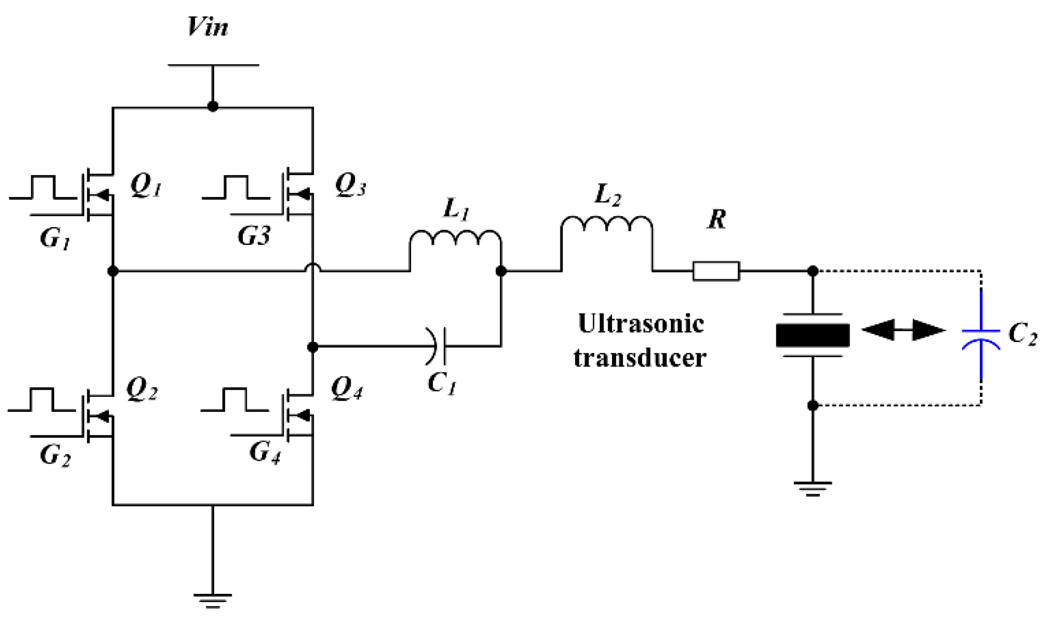
2. Fourth-Order LCLC Resonant Converter
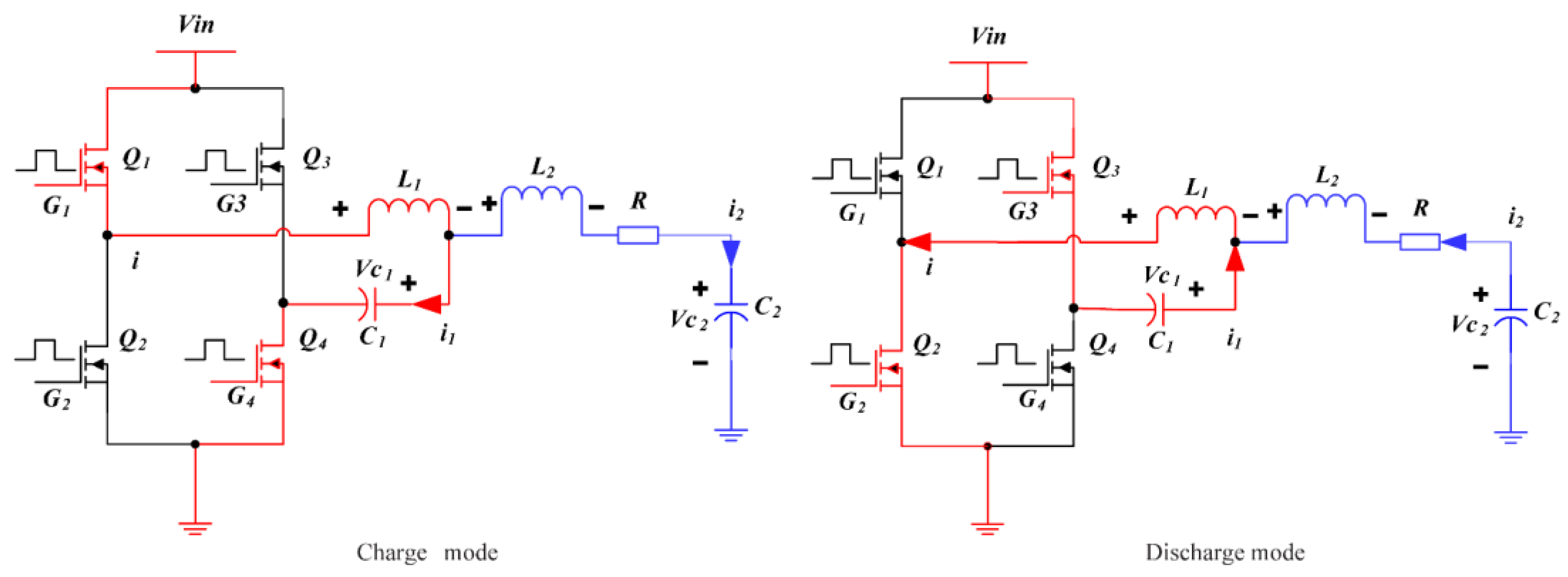
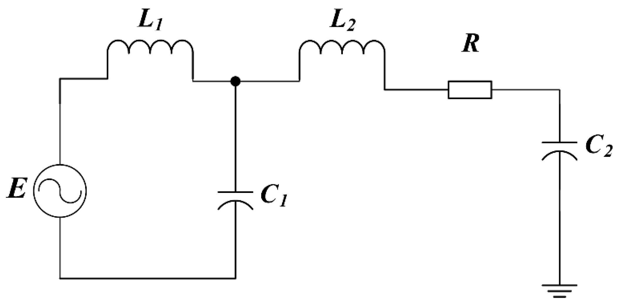
2.1. Circuit Description
2.2. Resonant Frequency
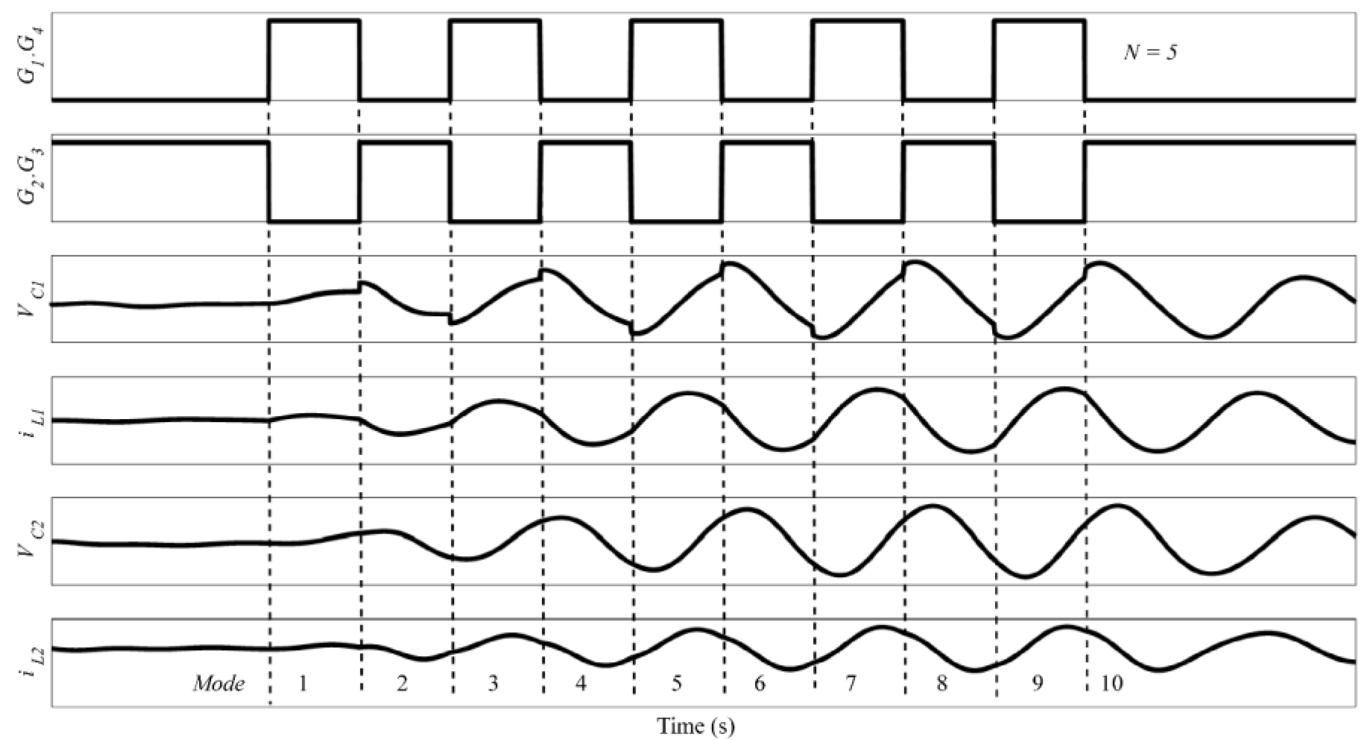
2.3. Circuit State Analysis
3. Analysis of Fourth-Order LCLC Resonant Converter
3.1. Analysis of Step-Up Ratio
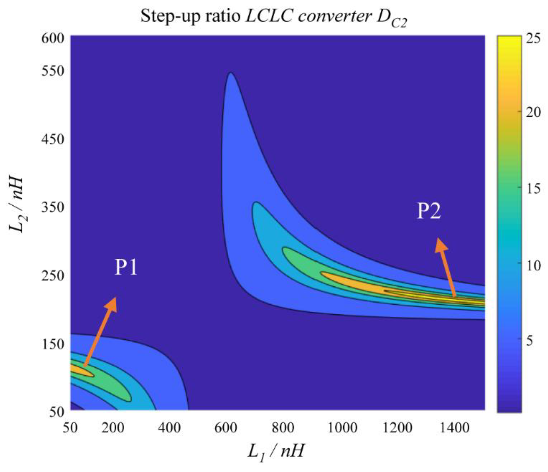
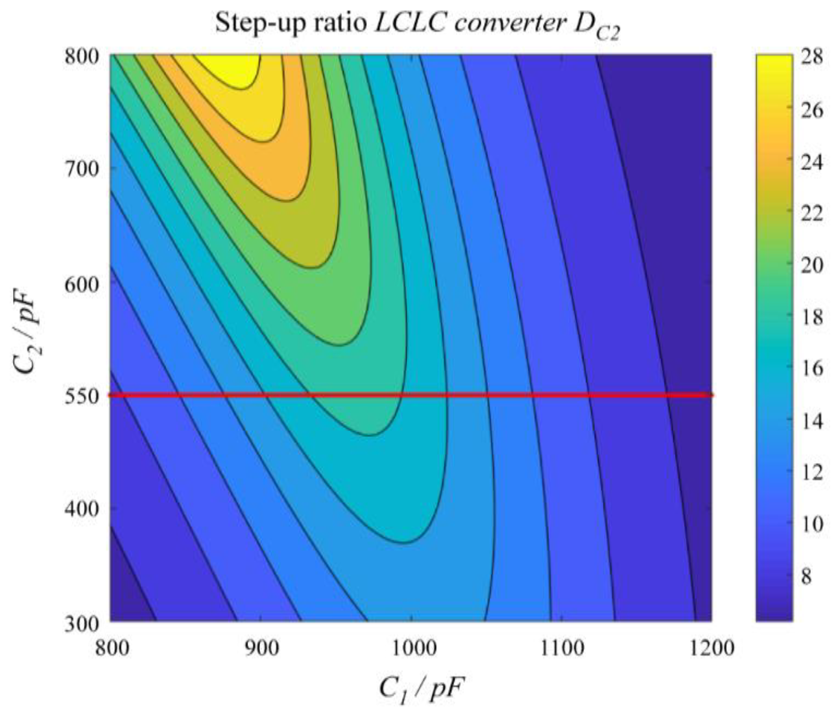
3.2. Analysis of Resonant Circuit Parameters
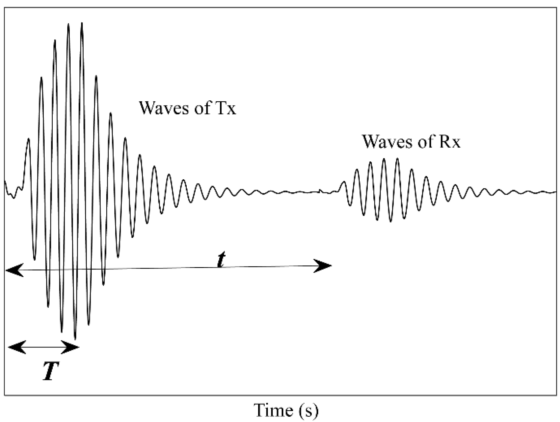
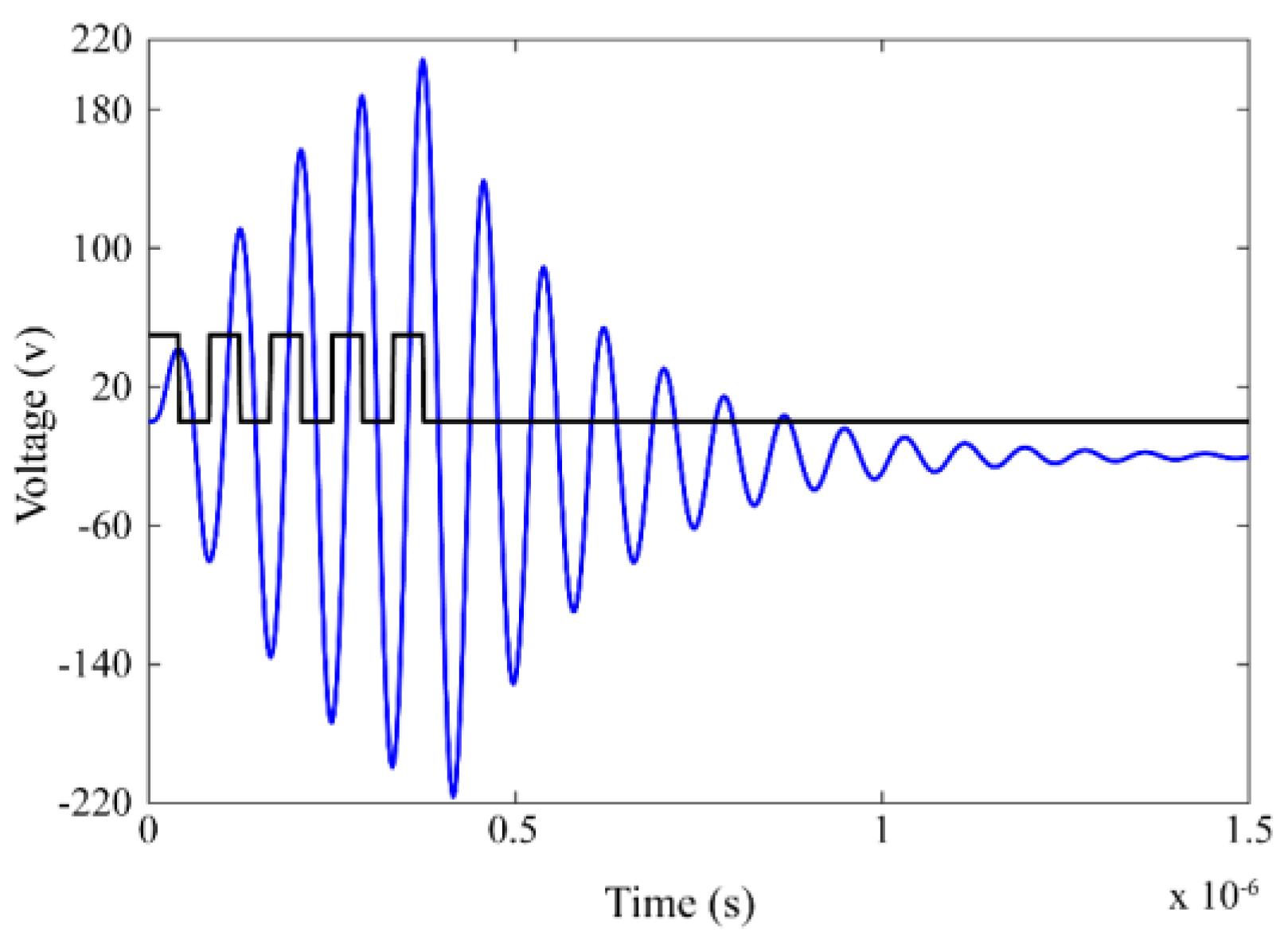
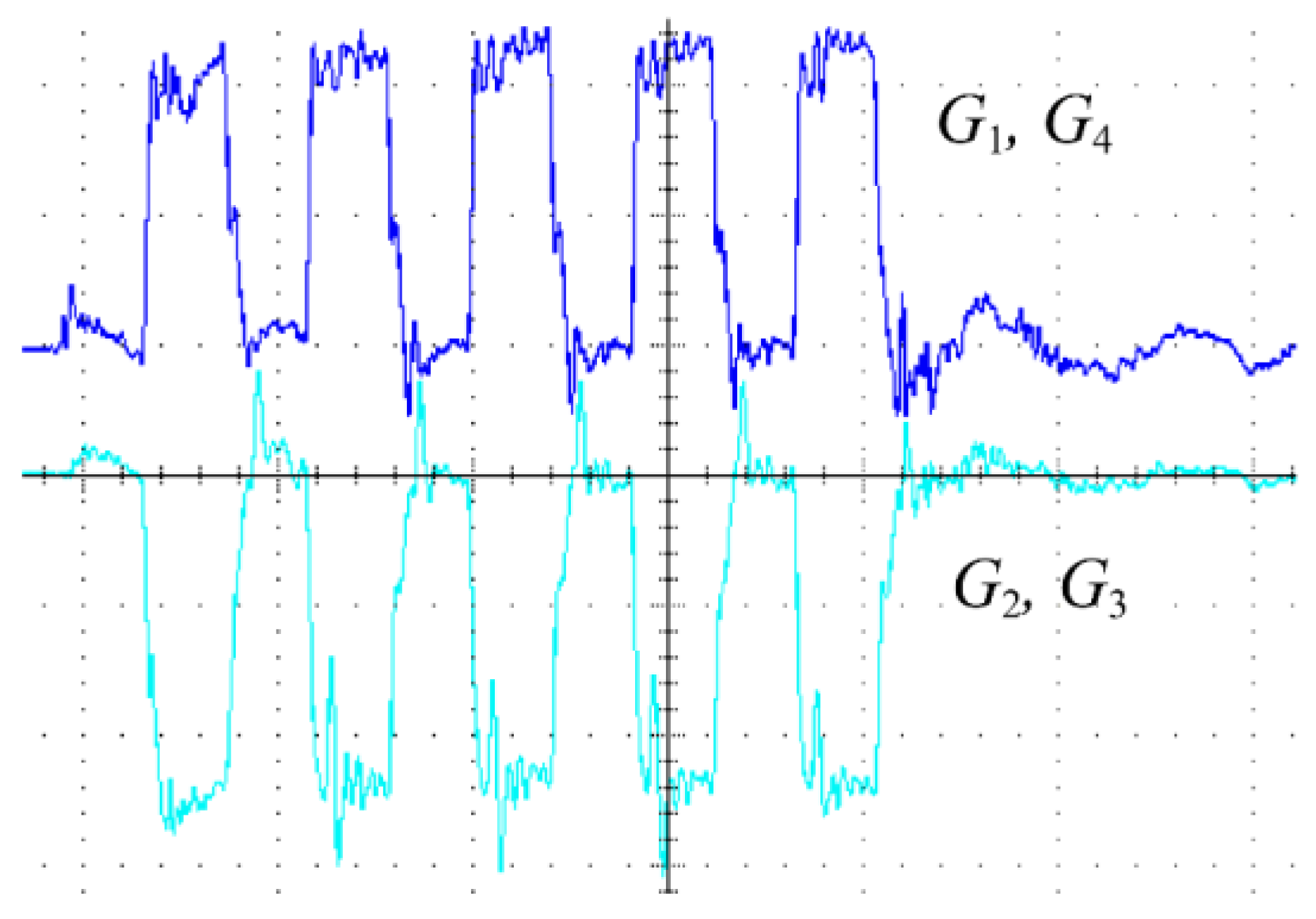
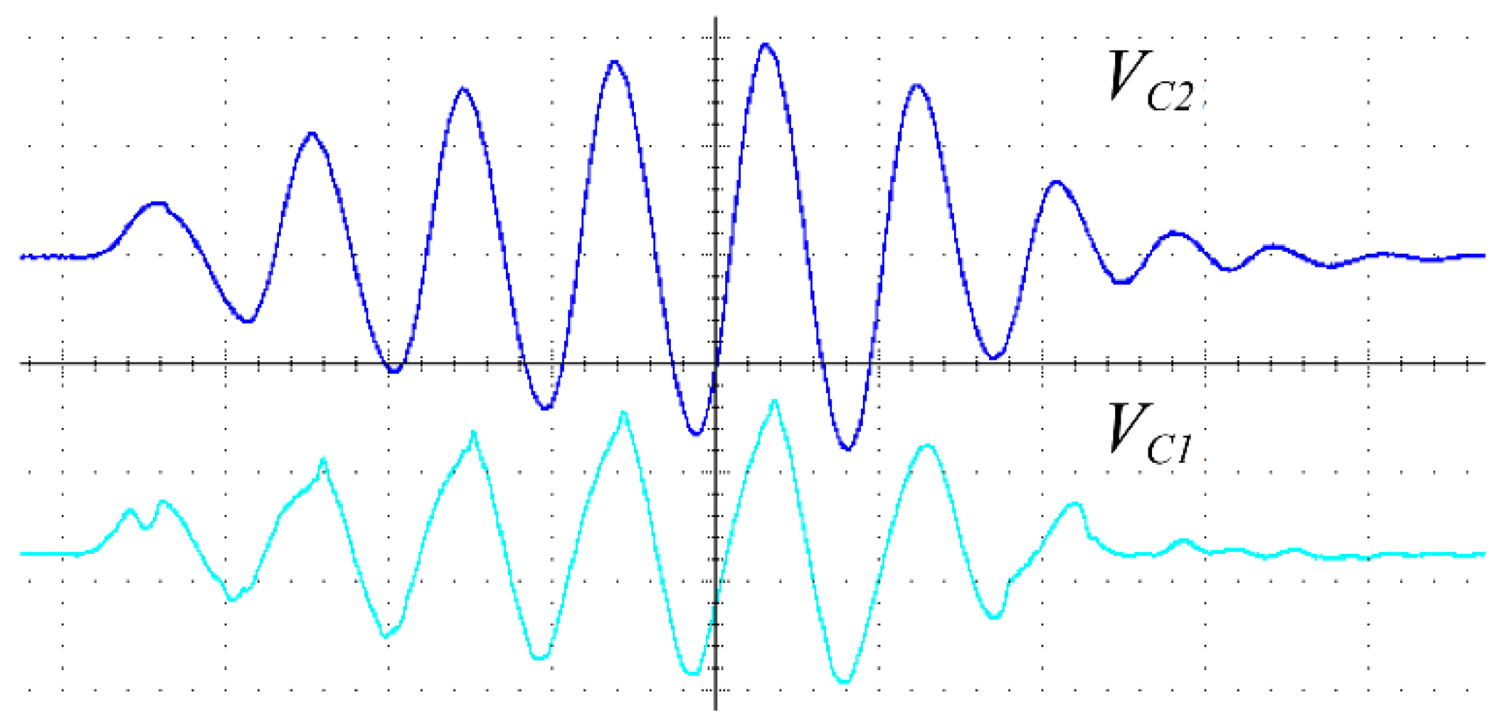
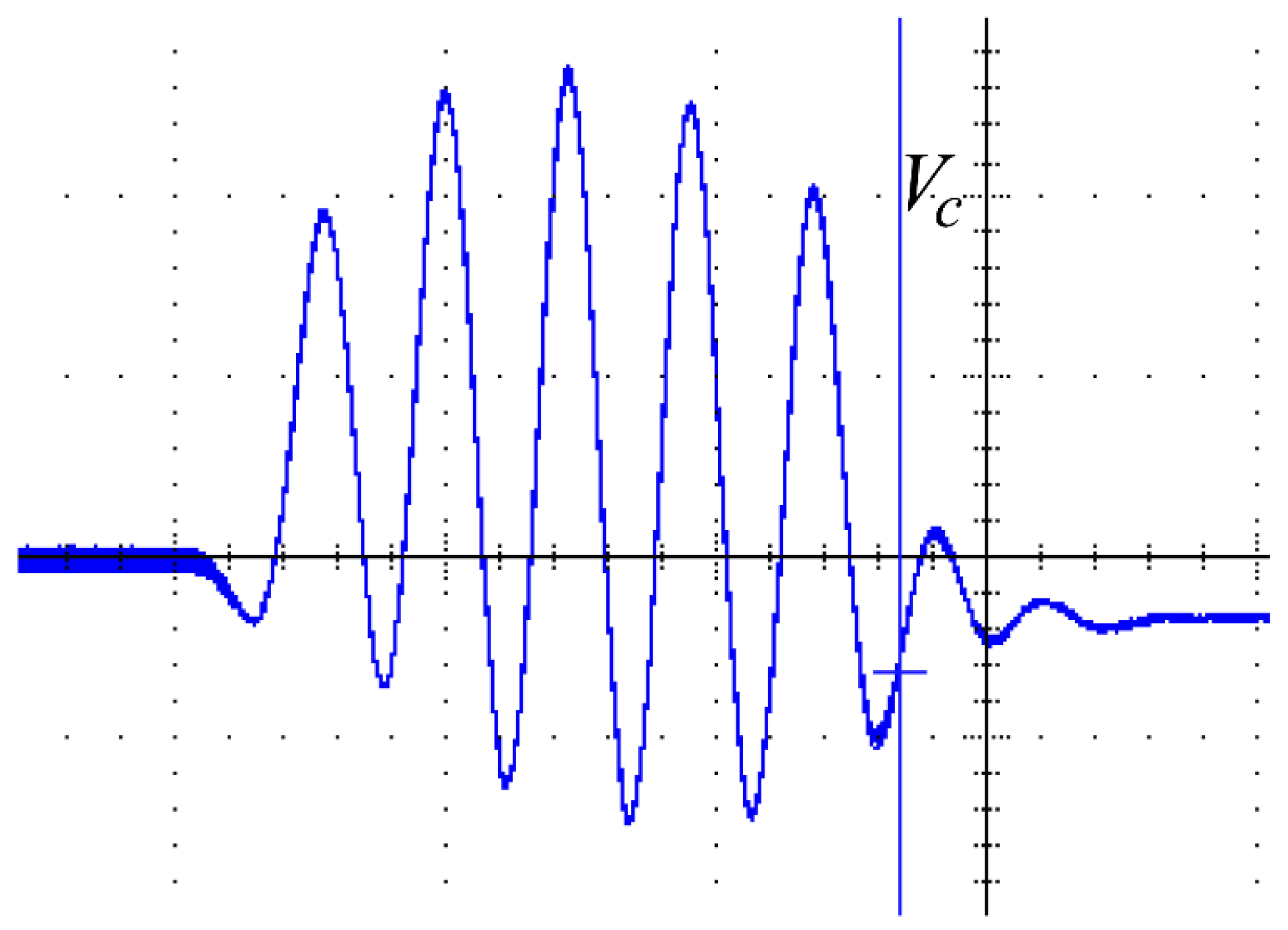
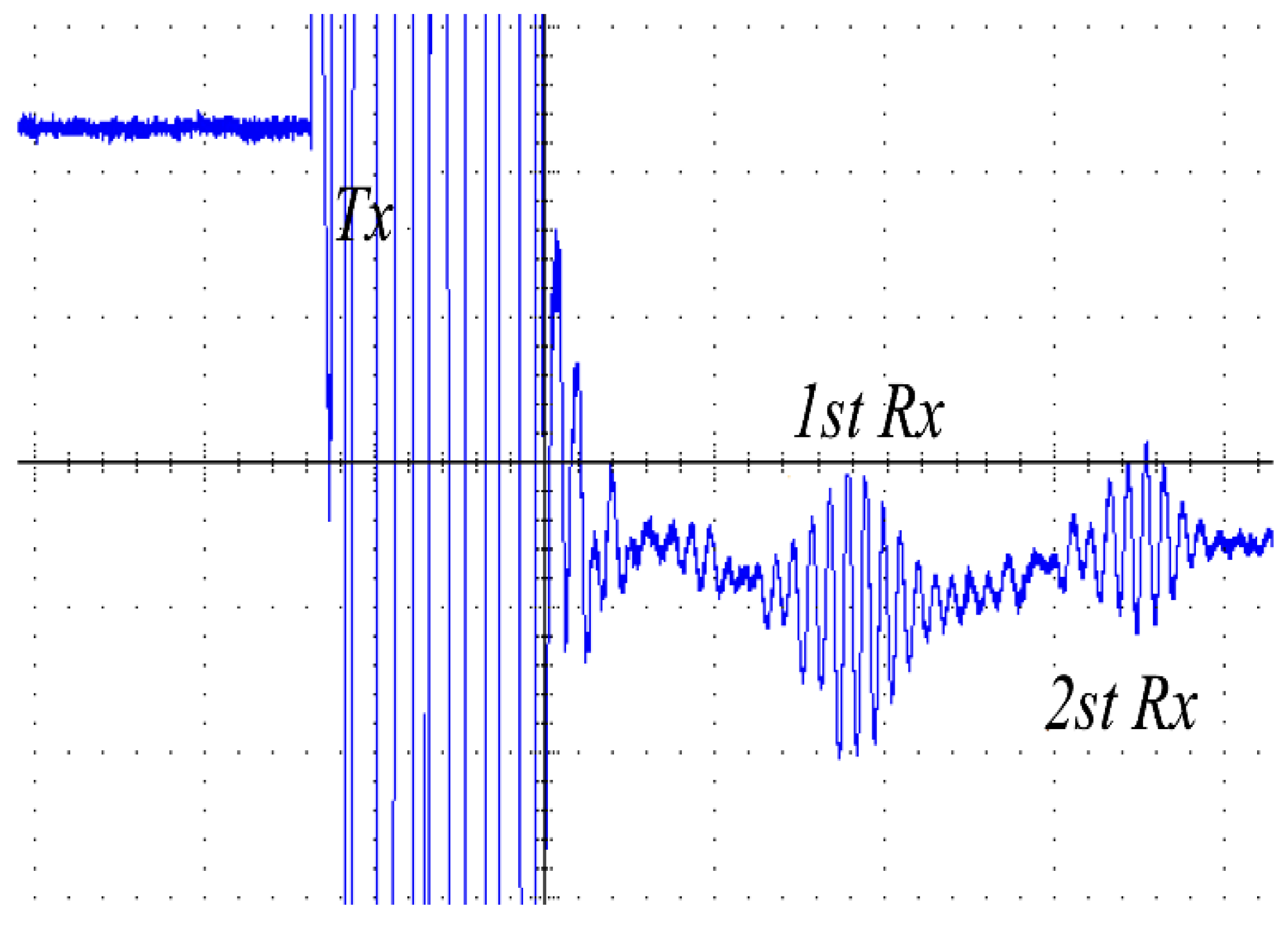
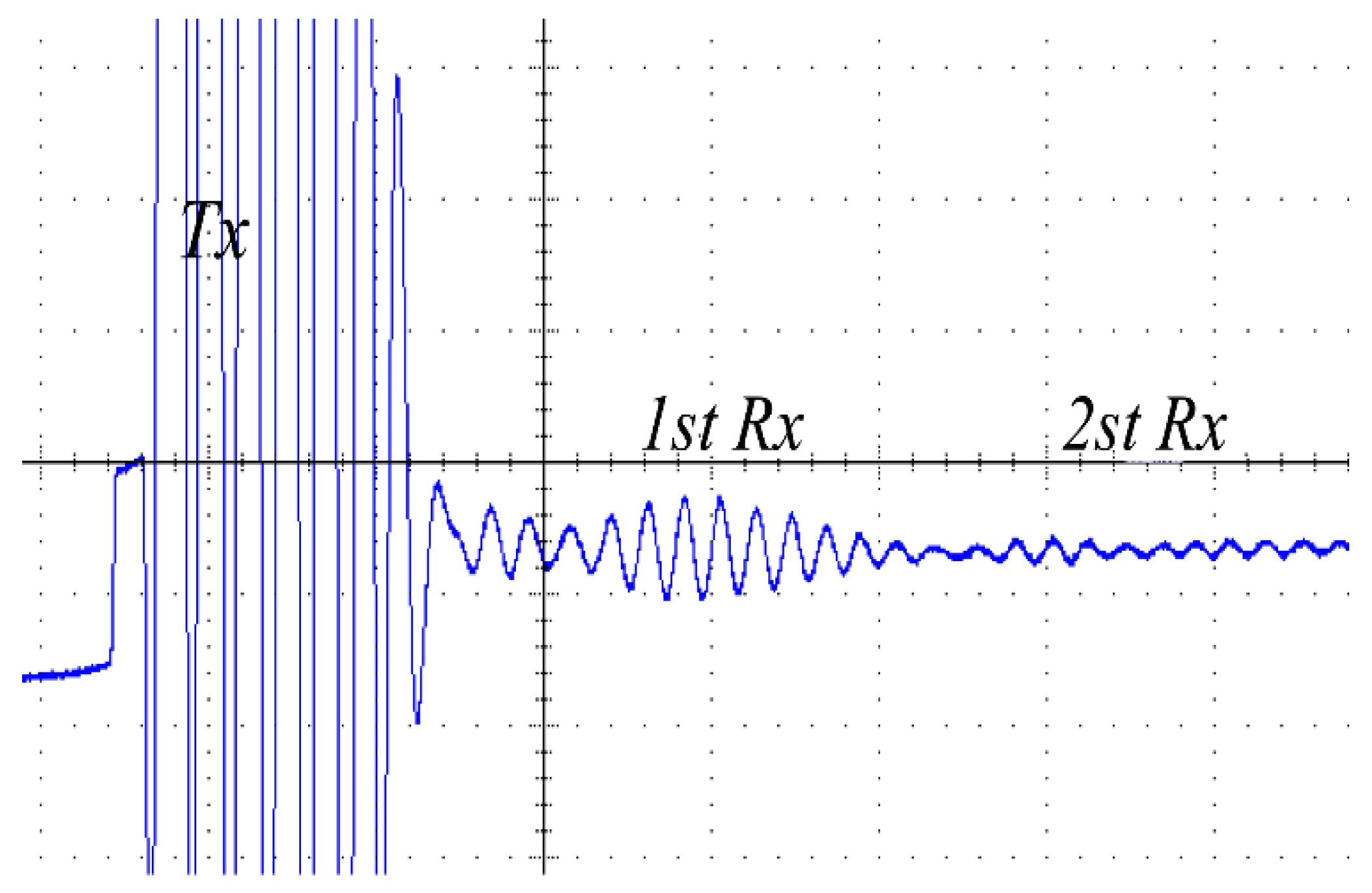
4. Experimental Results
5. Conclusions
Author Contributions
Funding
Institutional Review Board Statement
Informed Consent Statement
Data Availability Statement
Conflicts of Interest
References
- Tang, H.Y.; Lu, Y.; Jiang, X.; Ng, E.J.; Tsai, J.M.; Horsley, D.A.; Boser, B.E. 3-D Ultrasonic Fingerprint Sensor-on-a-Chip. IEEE J. Solid-State Circuits 2016, 51, 2522–2533. [Google Scholar] [CrossRef]
- Tang, H.-Y.; Lu, Y.; Assaderagh, F.; Daneman, M.; Jiang, X.; Lim, M.; Li, X.; Ng, E.; Singhal, U.; Tsai, J.M.; et al. 11.2 3D ultrasonic fingerprint sensor-on-a-chip. In Proceedings of the 2016 IEEE International Solid-State Circuits Conference, San Francisco, CA, USA, 31 January–4 February 2016; pp. 202–203. [Google Scholar] [CrossRef]
- Muralt, P.; Ledermann, N.; Paborowski, J.; Barzegar, A.; Gentil, S.; Belgacem, B.; Petitgrand, S.; Bosseboeuf, A.; Setter, N. Piezoelectric micromachined ultrasonic transducers based on PZT thin films. IEEE Trans. Ultrason. Ferroelect. Freq. Control 2005, 52, 2276–2288. [Google Scholar] [CrossRef] [PubMed]
- Seo, W.; Pi, J.-E.; Cho, S.H.; Kang, S.-Y.; Ahn, S.-D.; Hwang, C.-S.; Jeon, H.-S.; Kim, J.-U.; Lee, M. Transparent Fingerprint Sensor System for Large Flat Panel Display. Sensors 2018, 18, 293. [Google Scholar] [CrossRef] [PubMed]
- Nelson, R.B.; Erhart, R.A. Apparatus and Method for TFT Fingerprint Sensor. U.S. Patent 14 244 534, 3 April 2014. [Google Scholar]
- Alexander, K.; Kramer, A. Electrostatic Discharge Protection of a Capacitive Type Fingerprint Sensing Array. U.S. Patent 7 768 273, 3 August 2010. [Google Scholar]
- Hong, S.D. Embedded Active Matrix Organic Light Emitting Diode (AMOLED) Fingerprint Sensor. U.S. Patent 9 961 178, 1 May 2018. [Google Scholar]
- Yu, J.; Goh, W.L.; Arasu, M.A.; Je, M. A 60 V, >225 °C Half-Bridge Driver for Piezoelectric Acoustic Transducer, on SOI CMOS. IEEE Trans. Circuits Syst. II Express Briefs 2011, 59, 771–775. [Google Scholar]
- Horsley, D.A.; Rozen, O.; Lu, Y.; Shelton, S.; Guedes, A.; Przybyla, R.; Boser, B.E. Piezoelectric micro machined ultrasonic transducers for human-machine interfaces and biometric sensing. In Proceedings of the IEEE Sensors Conference, Busan, Korea, 1–4 November 2015; pp. 1–4. [Google Scholar]
- Yuan, T.; Dong, X.; Shekhani, H.; Li, C.; Maida, Y.; Tou, T.; Uchino, K. Driving an inductive piezoelectric transducer with class E inverter. Sens. Actuators A Phys. 2017, 261, 219–227. [Google Scholar] [CrossRef]
- Ma, K.-H.; Chang, W.-C.; Lee, Y.-C. A simple CLASS-E inverter design for driving ultrasonic welding system. In Proceedings of the 2009 International Conference on Power Electronics and Drive Systems (PEDS), Taipei, Taiwan, 2–5 November 2009; pp. 894–896. [Google Scholar] [CrossRef]
- Bi, C.; Lu, H.; Jia, K.; Hu, J.-G.; Li, H. A Novel Multiple-Frequency Resonant Inverter for Induction Heating Applications. IEEE Trans. Power Electron. 2016, 31, 8162–8171. [Google Scholar] [CrossRef]
- Hu, J.; Bi, C.; Jia, K.; Xiang, Y. Power Control of Asymmetrical Frequency Modulation in a Full-Bridge Series Resonant Inverter. IEEE Trans. Power Electron. 2015, 30, 7051–7059. [Google Scholar] [CrossRef]
- Agbossou, K.; Dion, J.-L.; Carignan, S.; Abdelkrim, M.; Cheriti, A. Class D amplifier for a power piezoelectric load. IEEE Trans. Ultrason. Ferroelectr. Freq. Control. 2000, 47, 1036–1041. [Google Scholar] [CrossRef] [PubMed]
- Giannelli, P.; Bulletti, A.; Granato, M.; Frattini, G.; Calabrese, G.; Capineri, L. A Five-Level, 1-MHz, Class-D Ultrasonic Driver for Guided-Wave Transducer Arrays. IEEE Trans. Ultrason. Ferroelectr. Freq. Control. 2019, 66, 1616–1624. [Google Scholar] [CrossRef] [PubMed]
- Dickinson, T.; Mathe, L.K.-A.; McCarthy, S.; Djordjev, K.D.; Oliveira, L.D.; Zhou, Q. Sensor Array with Receiver Bias Electrode. U.S. Patent 9 990 089, 5 June 2018. [Google Scholar]
- Djordjev, K.D.; Fennell, L.E.; Buchan, N.I.; Burns, D.W.; Gupta, S.K.; Bae, S. Display with Peripherally Configured Ultrasonic Biometric Sensor. U.S. Patent 933, 26 April 2016. [Google Scholar]


| Parameters | Symbols | Value |
|---|---|---|
| Input voltage | Vin | 20 V |
| Equivalent effective inductance 1 | L1 | 100 nH |
| Equivalent effective inductance 2 | L2 | 110 nH |
| Resonant capacitors 1 | C1 | 980 pF |
| Resonant capacitors 2 | C2 | 500 pF |
| ACF contact resistance | R | 5 Ω |
| Switching frequency | f | 12 MHz |
| Thickness of glass cover | s | 2 mm |
| MOSFET switches | Q1, Q1, Q3, Q4 | WSP4620 |
Disclaimer/Publisher’s Note: The statements, opinions and data contained in all publications are solely those of the individual author(s) and contributor(s) and not of MDPI and/or the editor(s). MDPI and/or the editor(s) disclaim responsibility for any injury to people or property resulting from any ideas, methods, instructions or products referred to in the content. |
© 2023 by the authors. Licensee MDPI, Basel, Switzerland. This article is an open access article distributed under the terms and conditions of the Creative Commons Attribution (CC BY) license (https://creativecommons.org/licenses/by/4.0/).
Share and Cite
Liu, W.; Shi, Y.; Sun, Z.; Zhang, L.; Zhang, Q. High Step-Up Ratio DC-AC Converter Using Fourth-Order LCLC Resonant Circuit for Ultrasonic Fingerprint-Sensor Drivers. Micromachines 2023, 14, 393. https://doi.org/10.3390/mi14020393
Liu W, Shi Y, Sun Z, Zhang L, Zhang Q. High Step-Up Ratio DC-AC Converter Using Fourth-Order LCLC Resonant Circuit for Ultrasonic Fingerprint-Sensor Drivers. Micromachines. 2023; 14(2):393. https://doi.org/10.3390/mi14020393
Chicago/Turabian StyleLiu, Wei, Yunlai Shi, Zhijun Sun, Li Zhang, and Qian Zhang. 2023. "High Step-Up Ratio DC-AC Converter Using Fourth-Order LCLC Resonant Circuit for Ultrasonic Fingerprint-Sensor Drivers" Micromachines 14, no. 2: 393. https://doi.org/10.3390/mi14020393
APA StyleLiu, W., Shi, Y., Sun, Z., Zhang, L., & Zhang, Q. (2023). High Step-Up Ratio DC-AC Converter Using Fourth-Order LCLC Resonant Circuit for Ultrasonic Fingerprint-Sensor Drivers. Micromachines, 14(2), 393. https://doi.org/10.3390/mi14020393