Communication

Dual Coupled Long-Range Hybrid Surface Plasmon Polariton Waveguide for Sub-Wavelength Confinement

1
School of Electronic Information and Artificial Intelligence, Shaanxi University of Science and Technology, Xi’an 710021, China
2
Key Laboratory for Wide Band Gap Semiconductor Materials and Devices of Education, School of Microelectronics, Xidian University, Xi’an 710071, China
*
Author to whom correspondence should be addressed.
Micromachines 2023, 14(12), 2167; https://doi.org/10.3390/mi14122167
Submission received: 5 November 2023 / Revised: 25 November 2023 / Accepted: 25 November 2023 / Published: 29 November 2023
(This article belongs to the Special Issue Advances in Optoelectronic Devices, 2nd Edition)

Abstract

:
In this paper, a long-range hybrid waveguide for subwavelength confinement based on double SPP coupling is proposed. The hybrid waveguide consists of a metal-based cylindrical hybrid waveguide and a silver nanowire. There are two coupling regions in the waveguide structure that enhance mode coupling. Strong mode coupling enables the waveguide to exhibit both a small effective mode area (0.01) and an extremely long transmission length (700 μm). The figure of merit (FOM) of the waveguide can be as high as 4000. In addition, the cross-sectional area of the waveguide is only 500 nm × 500 nm, allowing optical operation in the subwavelength range, which helps enhance the miniaturization of optoelectronic devices. The excellent characteristics of the hybrid waveguide make it have potential applications in photoelectric integrated systems.

1. Introduction

With the rapid development of optoelectronic integrated systems, the performance of optical devices is required to be higher [1,2]. A smaller device size is needed to improve circuit integration [3,4,5]. As the core component of an optoelectronic integrated system, waveguides need not only a longer transmission distance but also an extremely small mode area to enhance the integration and miniaturization of photoelectric integrated circuits [6,7,8,9]. In this context, designing sub-wavelength waveguides with excellent performance becomes a great challenge [10,11,12].
Traditional waveguides have a long transmission distance but poor light localization, which is not conducive to the design of small-sized devices [13,14]. Surface plasmon polaritons (SPPs) are a special electromagnetic wave excited at the interface between metal and medium [15,16,17,18]. SPP waves have excellent localization and can limit light to the range of sub-wavelength [19,20,21,22,23], which can be used to design small-sized and even sub-wavelength devices [24,25,26,27]. The combination of traditional waveguides with SPPs can be used to design waveguides with a long transmission distance and a small effective mode area. Nowadays, there are many kinds of SPP hybrid waveguides, and their performance has been greatly improved [28,29,30,31,32,33,34,35]. But with the rapid development of optoelectronic integrated systems, the requirement for waveguides is increasing [36,37,38]. New breakthroughs must be found to achieve good performance on small-sized devices.
In this paper, a high-performance hybrid waveguide at 1550 nm was designed using the double-reinforced coupling of metal SPP mode and silicon waveguide mode. The hybrid waveguide consists of a metal-based cylindrical hybrid waveguide and a silver nanowire. The two coupling regions in the waveguide structure enhance the modal coupling. The strong mode coupling makes the light field locally compact, and the waveguide shows an extremely small effective mode area. Therefore, the hybrid waveguide combines the long transmission length of the silicon waveguide with the small mode area of the SPP wave. In addition, the waveguide realizes the sub-wavelength operation of light.

2. Structure Design

The hybrid waveguide consists of a metal-based cylindrical hybrid waveguide and silver nanowires. Figure 1a is a schematic diagram of a metal-based cylindrical hybrid waveguide. The cylindrical silver nanowire passes through the center of the silicon waveguide, and the void region is filled with silicon dioxide. The radius of the silver nanowire is labeled rAg. The thickness of the silicon dioxide and silicon layer is labeled as tSiO2 and tSi, respectively.
Figure 1b shows the hybrid waveguide proposed in this paper. A silver nanowire with a radius of RAg was placed above the metal-based cylindrical hybrid waveguide. The spacing between silver nanowire and metal-based cylindrical hybrid waveguides is g. The whole structure of the hybrid waveguide is covered by SiO2 cladding. In this paper, the waveguide was studied at the 1550 nm communication wavelength.

3. Methods

The proposed metal-based cylindrical hybrid waveguide realizes the double coupling of silicon waveguide mode and SPP mode in its structure. The superposition and strengthening of coupling are helpful to improve the waveguide characteristics, making the performance of the waveguide better than other existing hybrid waveguides.
A waveguide is an important part of an optoelectronic system, and its performance affects other waveguide-based optoelectronic devices [39,40]. In practical applications, the requirements of a waveguide include a small size, a long transmission distance, and a small mode area. The main parameters used to evaluate waveguide characteristics include effective mode area, transmission length, figure of merit, and modal effective index [41,42]. The formulas for calculating each parameter are discussed in detail below.
Effective mode area (Aeff) characterizes the localization of light in a waveguide. The value of Aeff is expected to be as small as possible in the design of the waveguide. A smaller Aeff means that the light field is more concentrated in the waveguide and quickly disappears in the direction perpendicular to the transmission (longitudinal). Aeff is calculated by the following formula [14,42]:
A e f f = + W x , y d x d y / m a x W x , y
According to the above formula, Aeff is the ratio of total energy to maximum energy density. The electromagnetic energy density can be calculated using the following formula [43]:
W x , y = 1 2 R e d ω ε x , y d ω E x , y 2 + 1 2 μ 0 H x , y 2
where H(x,y) is the magnetic field and E(x,y) is the electric field. The normalized effective modal area Aeff/A0, where A0 = λ2/4, is commonly used to evaluate the characteristics of waveguides.
The transmission length (Lm) of a waveguide is defined as the distance that light travels when the energy decays to 1/e of its initial value. Lm can be calculated using the following equation [8,44]:
L m = λ / 4 π Im N e f f
where Neff is the modal effective index, Neff = neff + I × αeff. αeff is the imaginary part of Neff, which represents the loss of light in the waveguide. It can be defined as αeff = Im(Neff). Aeff and Lm are two opposing parameters. A smaller effective modal area results in a shorter transmission length. There is generally an appropriate balance between Lm and Aeff. Thus, the figure of merit (FOM) provides a measure of compromise. The calculation formula for FOM is as follows:
F O M = L m 2 A e f f π

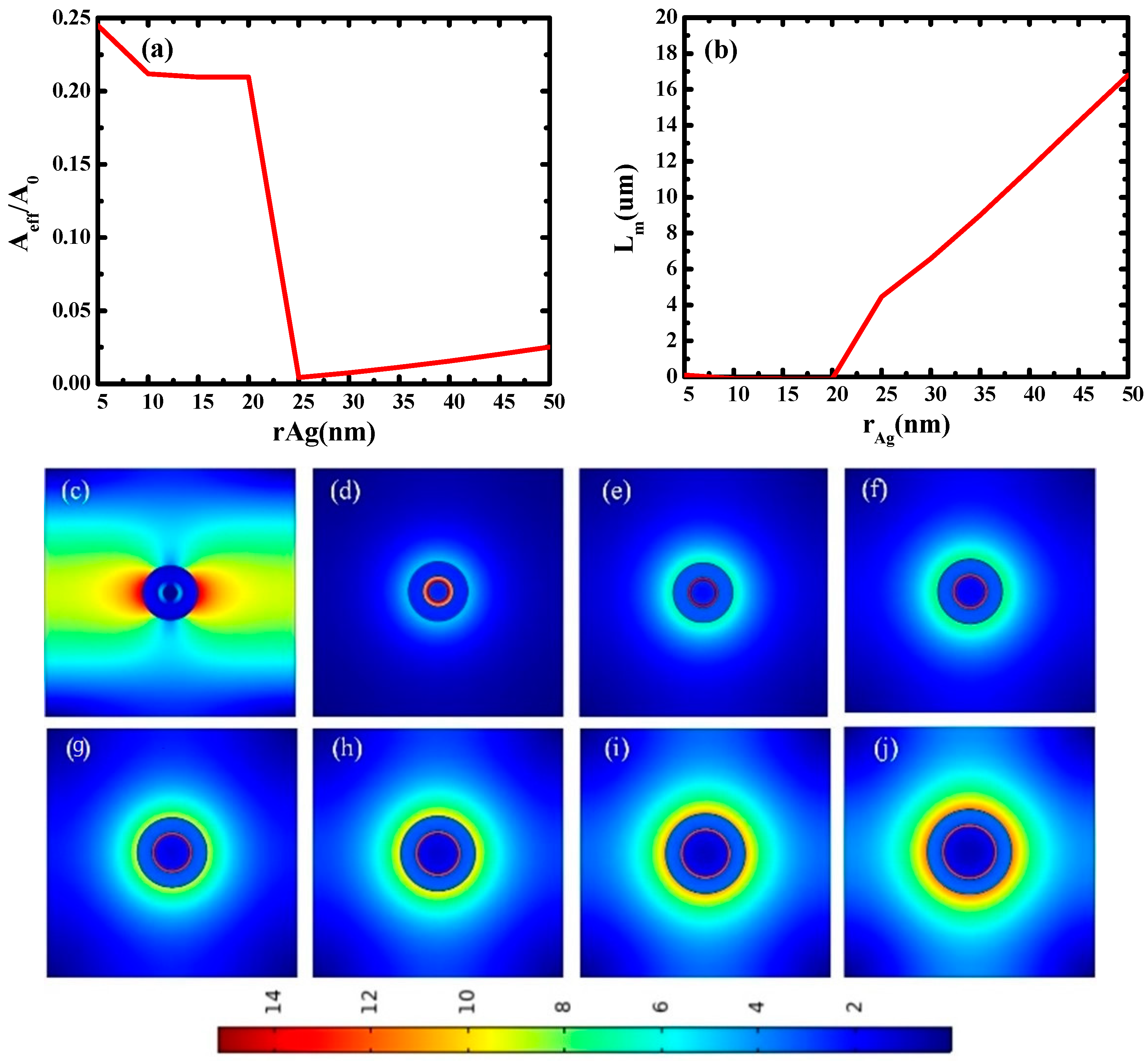
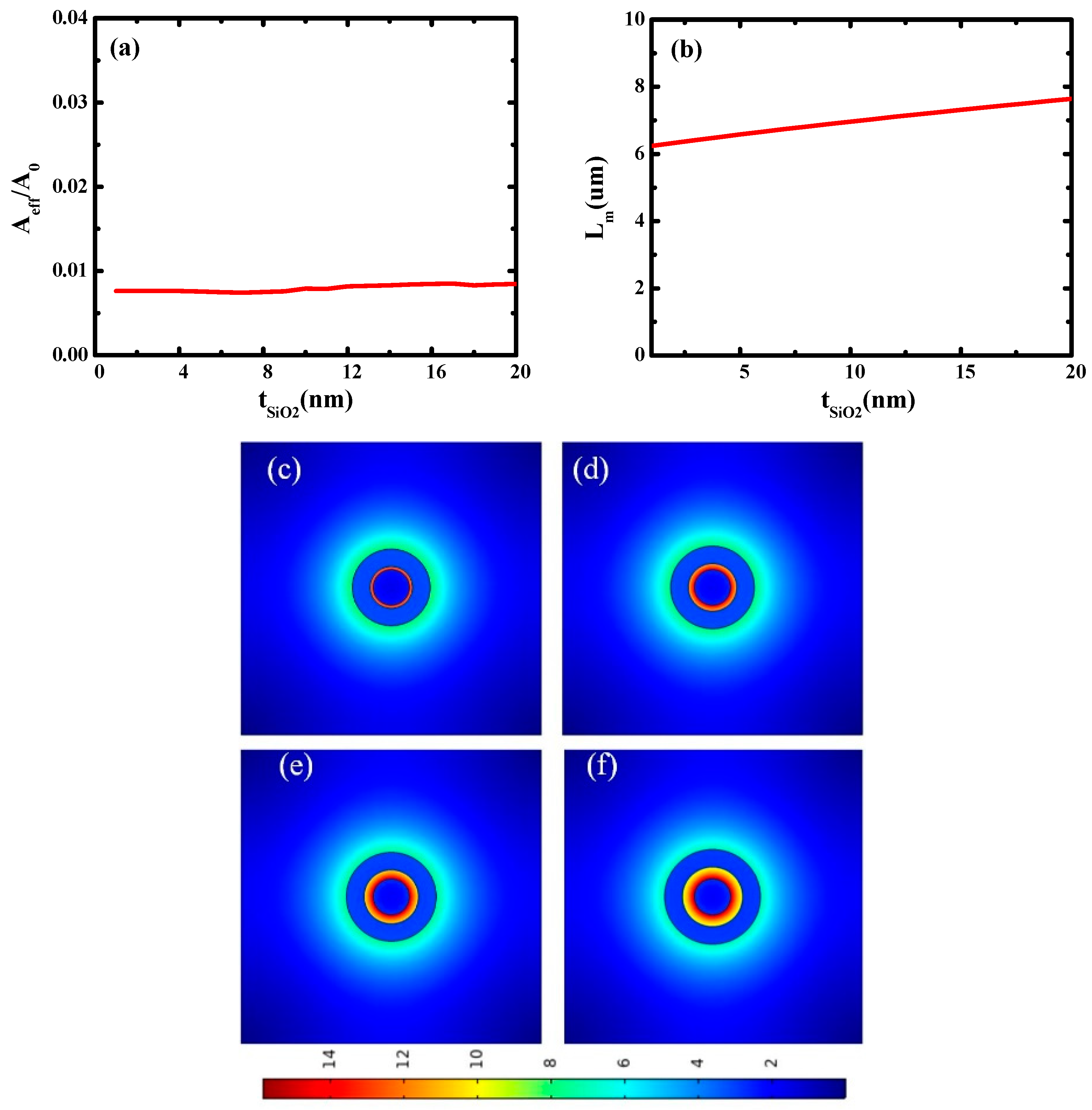
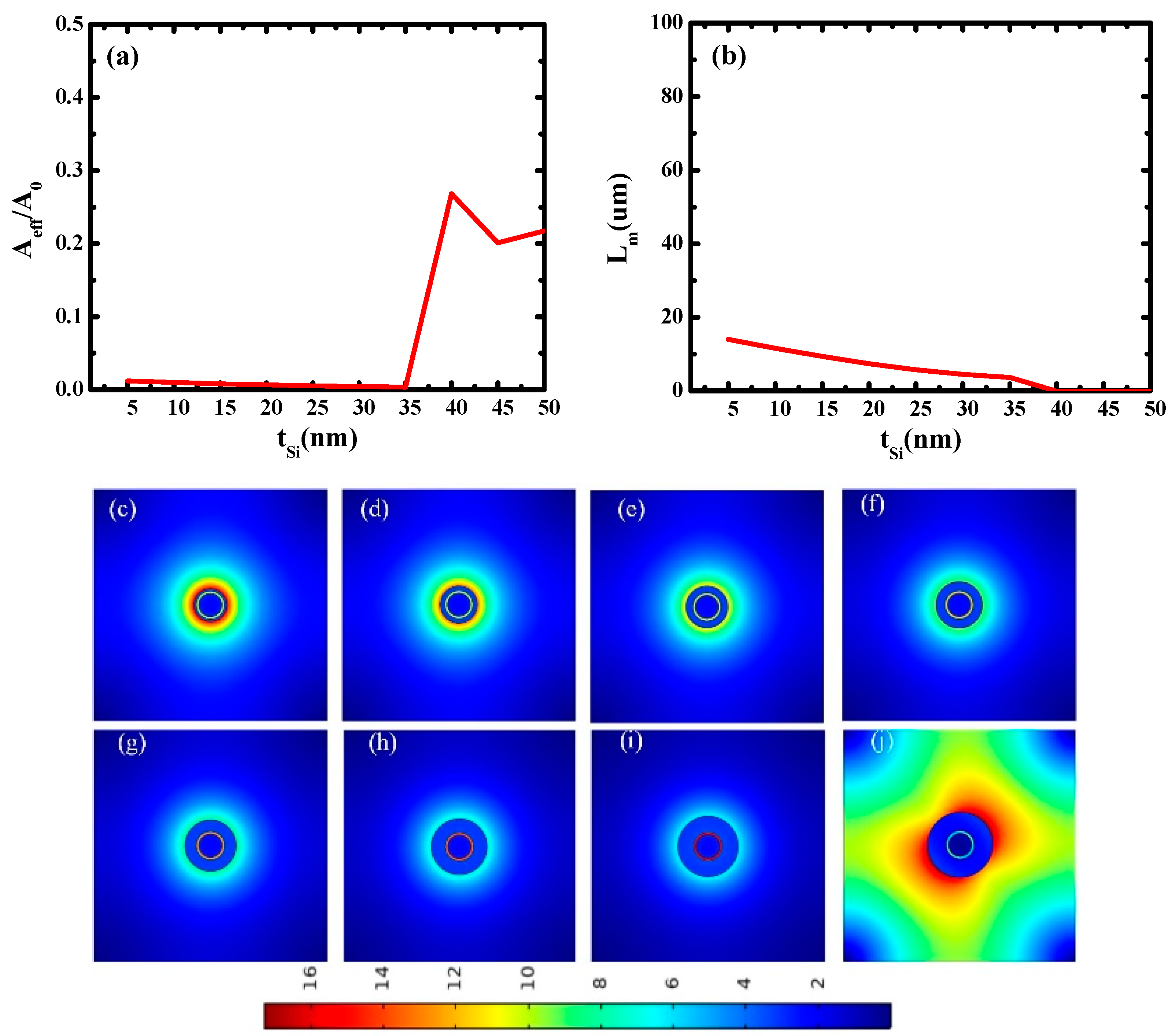
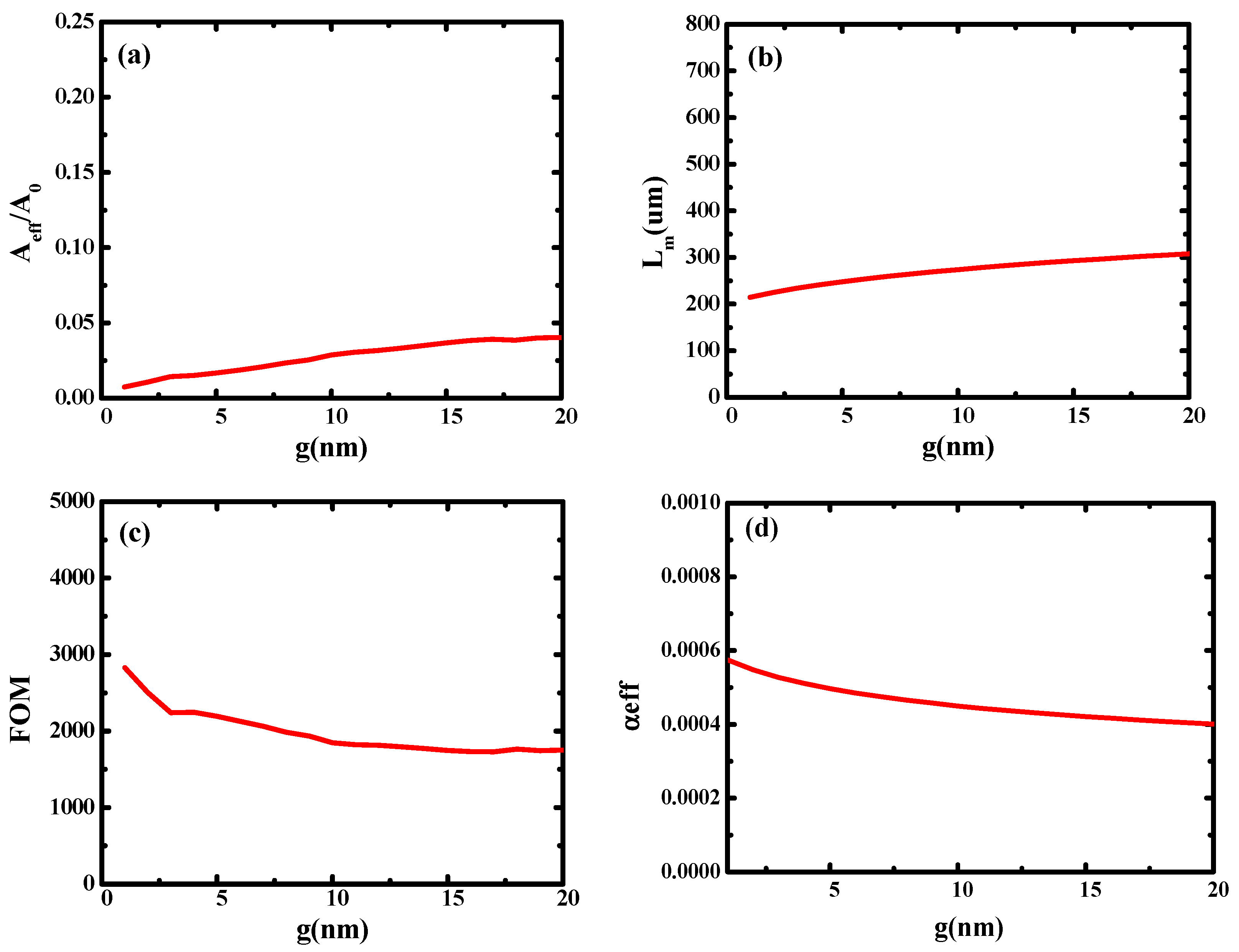
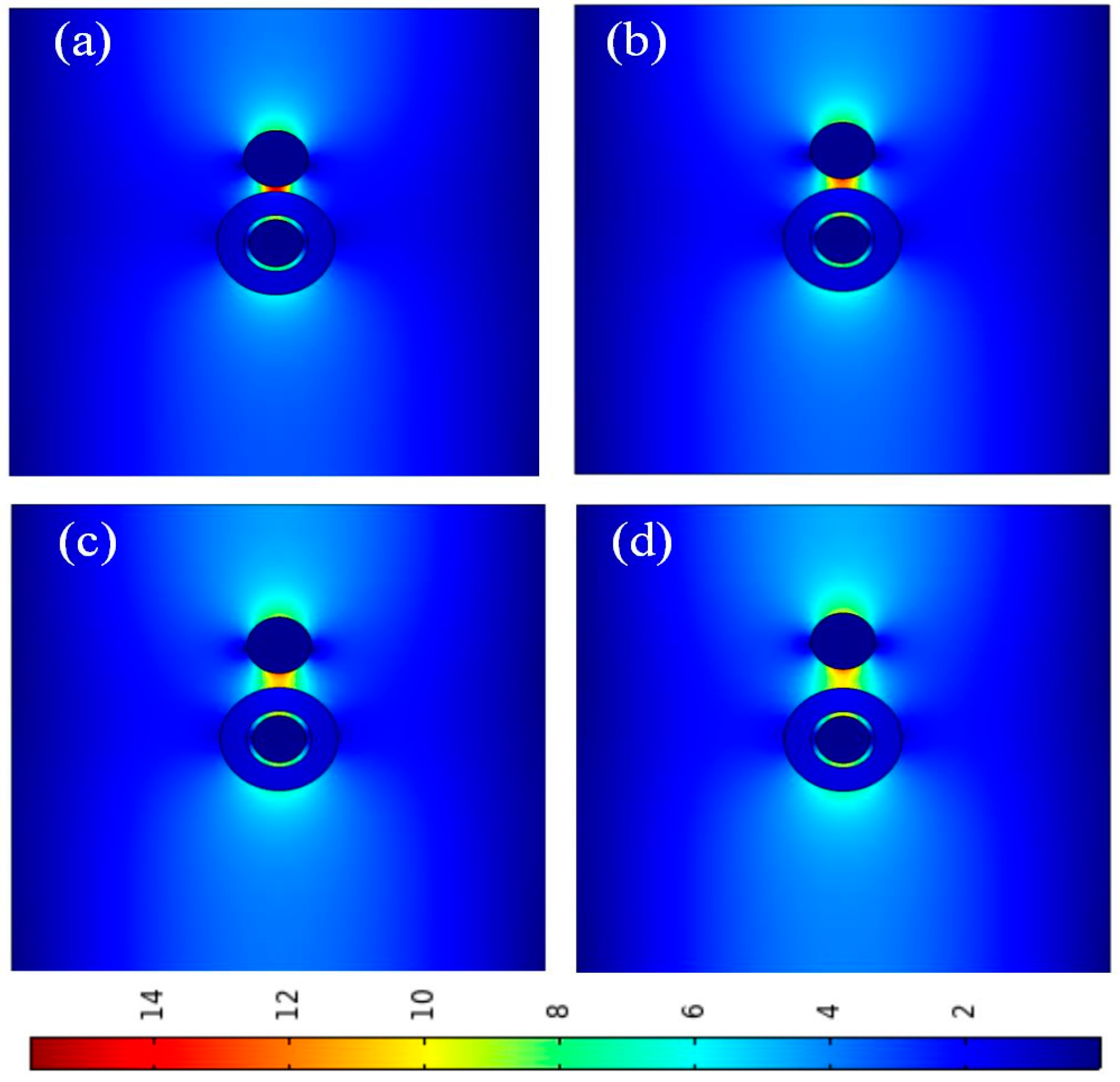
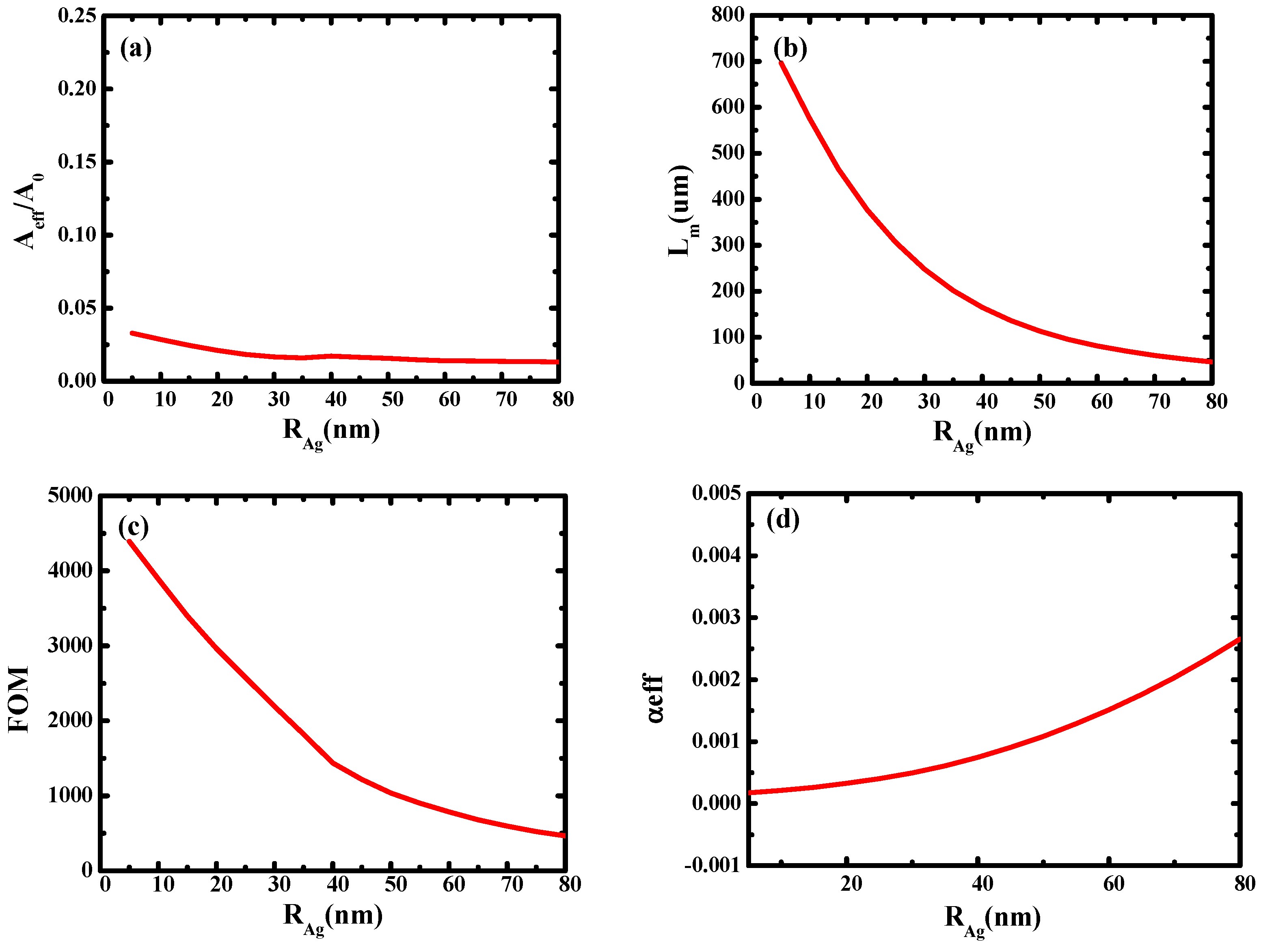
4. Results and Discussion

In this paper, the metal-based cylindrical hybrid waveguide was examined first, which consists of a cylindrical silver nanowire passing through the center of the silicon waveguide with a SiO2 gap between the silver nanowire and Si. The good characteristics of the waveguide were obtained through mode coupling of the silicon photonic mode with the silver nanowire SPP mode.
The waveguide was studied at the working wavelength of 1550 nm. We improved the waveguide’s performance by optimizing its geometric parameters. The characteristic parameters and electric field distribution of the waveguide were simulated by COMSOL Multiphysics software 5.4. At the 1550 nm working wavelength, the relative permittivity of Ag, Si, and SiO2 is −129 + 3.3i, 12.25, and 2.25, respectively [42,45].
Firstly, the propagation characteristics of waveguides with different silver nanowire radii (rAg) were studied. In this simulation, tSiO2 and tSi are fixed at 5 nm and 25 nm, and rAg varies from 5 nm to 50 nm. As illustrated in Figure 2a,b, the normalized effective mode area (Aeff/A0) is very high below 20 nm, decreases rapidly after 20 nm, and then increases slightly after 25 nm. Lm, however, has the opposite trend. The main reason for these phenomena is that when rAg is less than 20 nm, the radius of silver nanowire is too small and no mode coupling occurs, so the mode area is large and the optical transmission length is extremely short because of the heavy loss. After 25 nm, the coupling weakens with the increase in rAg, so Aeff/A0 increases.
Figure 2c–j shows the electric field distributions of waveguides at different silver nanowire radii (rAg), and the electric field distribution refers to the magnitude of the total electric field. It can be seen that when rAg = 20 nm, the electric field distribution is diffused in the cladding, and no mode coupling occurs. When rAg is equal to or greater than 25 nm, mode coupling occurs, and a strong electric field is concentrated in the SiO2 gap region. With the increase in rAg, mode coupling weakens, and electric field localization weakens. These results agree well with the calculated data in Figure 2a,b. In the subsequent simulation, rAg is set to 25 nm.
Next, the characteristics of the waveguide on SiO2 thicknesses (tSiO2) were studied. In this simulation, rAg is fixed at 25 nm and tSi is fixed at 30 nm, and tSiO2 varies from 1 nm to 20 nm. The results are shown in Figure 3a,b. It can be seen that with the increase in SiO2 thickness, the normalized effective mode area (Aeff/A0) and transmission length of the hybrid waveguide increase slightly. This is because larger SiO2 gaps will result in weaker mode coupling.
Figure 3c–f shows the electric field distribution of the metal-based cylindrical hybrid waveguide at different tSiO2. It can be seen that the electric field in Figure 3c is well localized, and electric field localization gradually weakens with the increase in tSiO2, which is in good agreement with Figure 3a,b. According to these simulation results, the optimal size of tSiO2 is 5 nm.
Then, the influence of silicon thickness (tSi) on waveguide characteristics was studied. rAg and tSiO2 are fixed at 25 nm and 5 nm, respectively. tSi ranges from 5 nm to 50 nm. The results are shown in Figure 4. When tSi is less than 35 nm, both the normalized effective mode area and the transmission distance decrease gradually, which is because the increase in silicon thickness leads to the enhancement of mode coupling, then optical localization increases and transmission length decreases. When tSi is greater than 35 nm, the normalized effective modal area increases rapidly, and the transmission distance decreases rapidly. This is because there is no mode coupling in the waveguide when tSi is in this interval, and light field dispersion causes serious loss, so the transmission distance is extremely small.
Figure 4c–j shows the electric field distributions at different silicon thicknesses (tSi). As illustrated in Figure 4c–i, with the increase in tSi, mode coupling becomes stronger, and the electric field becomes more localized. Figure 4j shows the electric field distribution at tSi = 40 nm. It can be seen that no mode coupling occurs at tSi = 40 nm, and the electric field is dispersed throughout the waveguide structure. These results are consistent with Figure 4a,b. The optimal value of tSi is 35 nm.
Then, on the basis of the metal-based cylindrical hybrid waveguide, we introduced dual-mode coupling, investigated its performance in detail, and optimized its geometric parameters. The structure of the dual-coupled hybrid waveguide is shown in Figure 1b. According to the simulation results of the metal-based cylindrical hybrid waveguide, the optimized structural parameters are tSi = 35 nm, rAg = 25 nm, tSiO2 = 5 nm, and RAg = 30 nm. Firstly, the influence of gap height (g) on hybrid waveguide performance was studied. As shown in Figure 5, with the increase in gap height (g), both the normalized effective modal area and the transmission length increase. Figure 5c shows the quality factor of the waveguide (FOM). Figure 5d shows the loss of light in the waveguide (αeff), and its change trend is opposite that of Lm. The main reason is that the mode coupling weakens with the increase in g, resulting in the weakening of optical localization, so Aeff/A0 increases and the transmission length of light increases. It can be seen that the double coupling of modes improves the performance of the waveguide significantly. The transmission length increases by an order of magnitude while the normalized mode area remains small, and FOM increases by 20 times.
Figure 6 shows the electric field distributions of waveguides at different gap heights (g). We can see that with an increase in g, the localization of the electric field decreases, and the electric field distribution becomes more dispersed. Due to the double coupling of the modes, the electric field is mainly concentrated in the SiO2 gap region between silver and silicon. The electric field is most concentrated at g = 5 nm. The results are consistent with Figure 5, so the best value for g is 5 nm.
Then, the influence of silver nanowire radius (RAg) on waveguide performance was studied. As shown in Figure 7, it can be seen that with the increase in RAg, the effective mode area and transmission length both decrease due to the enhancement of mode coupling. It can be concluded that an ultra-small area (0.01) and an ultra-long transmission length (700 μm) can be obtained by optimizing RAg, and FOM can reach 4000.
To further verify the above calculation results, Figure 8 lists the electric field distributions of the waveguide at different silver nanowire radii. It can be seen that as RAg increases, the electric field becomes more concentrated, and mode coupling becomes stronger. According to the results in Figure 7 and Figure 8, we made a compromise between Aeff/A0 and Lm and finally chose the value of RAg as 30 nm.
Based on the above research results, it can be concluded that the optimal size of the proposed dual-coupled hybrid waveguide is rAg = 25 nm, tSiO2 = 5 nm, tSi = 35 nm, g = 5 nm, and RAg = 30 nm. Under these conditions, the hybrid waveguide shows excellent waveguide characteristics.

5. Conclusions

In conclusion, we proposed a hybrid waveguide based on metal SPPs at 1550 nm. By adopting two coupling regions in the waveguide structure, extremely strong mode coupling is achieved. The results show that the hybrid waveguide has excellent performance, such as a small effective mode area of 0.01 and a long transmission length of 700 μm. In addition, the figure of merit (FOM) can be as high as 4000, and the cross-sectional area of the waveguide is 500 nm × 500 nm, which enables optical manipulation in the sub-wavelength range. These excellent characteristics enable our proposal to have great potential in optoelectronic integrated systems.

Author Contributions

Conceptualization, Y.W.; methodology, S.W.; software, J.Z. and M.X. All authors have read and agreed to the published version of the manuscript.

Funding

This research was funded by the Natural Science Basic Research Program of Shaanxi, grant number 2022JQ-634, and the Scientific Research Plan of the Shaanxi Education Department, grant number 22JK0301.

Data Availability Statement

Data are contained within the article.

Acknowledgments

We acknowledge Dong Lu and Qu Sheng for their contributions to this manuscript.

Conflicts of Interest

The authors declare no conflict of interest.

References

  1. Chandra, V.; Ranjan, R. Performance analysis of different slot waveguide structures for evanescent field based gas sensor applications. Opt. Quantum Electron. 2021, 53, 457. [Google Scholar] [CrossRef]
  2. Wang, Y.; Liu, H.; Wang, S.; Cai, M. Hybrid Nanowire–Rectangular Plasmonic Waveguide for Subwavelength Confinement at 1550 Nm. Micromachines 2022, 13, 1009. [Google Scholar] [CrossRef]
  3. Piels, M.; Bowers, J.E. Photodetectors for silicon photonic integrated circuits. In Photodetectors; Elsevier: Amsterdam, The Netherlands, 2023; pp. 419–436. [Google Scholar] [CrossRef]
  4. Ye, Z.; Tan, C.; Huang, X.; Ouyang, Y.; Yang, L.; Wang, Z.; Dong, M. Emerging MoS2 Wafer-Scale Technique for Integrated Circuits. Nano-Micro Lett. 2023, 15, 38. [Google Scholar] [CrossRef] [PubMed]
  5. Zhang, Y.; Wu, J.; Jia, L.; Qu, Y.; Yang, Y.; Jia, B.; Moss, D.J. Graphene oxide for nonlinear integrated photonics. Laser Photonics Rev. 2023, 17, 2200512. [Google Scholar] [CrossRef]
  6. Hu, Y.; Zhang, Y.; Su, G.; Zhao, M.; Li, B.; Liu, Y.; Li, Z. Realization of ultrathin waveguides by elastic metagratings. Commun. Phys. 2022, 5, 62. [Google Scholar] [CrossRef]
  7. Liu, L.; Yang, Y.; Yu, C.; Li, S.; Wu, H.; Sun, L.; Meng, F. A substrate integrated waveguide-based W-band antenna for microwave power transmission. Micromachines 2022, 13, 986. [Google Scholar] [CrossRef]
  8. Wang, Y.; Wang, S.; Cai, M.; Liu, H. A long propagation distance hybrid triangular prism waveguide for ultradeep subwavelength confinement. IEEE Sens. J. 2019, 19, 11159–11166. [Google Scholar] [CrossRef]
  9. Adhikari, R.; Sbeah, Z.; Chauhan, D.; Chang, S.H.; Dwivedi, R.P. A voyage from plasmonic to hybrid waveguide refractive index sensors based on wavelength interrogation technique: A review. Braz. J. Phys. 2022, 52, 61. [Google Scholar] [CrossRef]
  10. Ozcan, C.; Aitchison, J.S.; Mojahedi, M. Optimization of bulk sensitivity for strip, slot, and subwavelength grating-based waveguides for dual-polarization operation. Opt. Express 2023, 31, 3579–3594. [Google Scholar] [CrossRef]
  11. Chen, Y.; Zheng, X.; Zhang, X.; Pan, W.; Wang, Z.; Li, S.; Dong, S.; Liu, F.; He, Q.; Zhou, L. Efficient Meta-couplers Squeezing Propagating Light into On-Chip Subwavelength Devices in a Controllable Way. Nano Lett. 2023, 23, 3326–3333. [Google Scholar] [CrossRef]
  12. Sun, H.; Chen, L.R. Polarization independent Bragg gratings using tilted subwavelength grating waveguide Bragg gratings. Opt. Express 2023, 31, 1214–1223. [Google Scholar] [CrossRef] [PubMed]
  13. Dionne, J.; Sweatlock, L.; Atwater, H.; Polman, A. Plasmon slot waveguides: Towards chip-scale propagation with subwavelength-scale localization. Phys. Rev. B 2006, 73, 035407. [Google Scholar] [CrossRef]
  14. Oulton, R.F.; Sorger, V.J.; Genov, D.; Pile, D.; Zhang, X. A hybrid plasmonic waveguide for subwavelength confinement and long-range propagation. Nat. Photonics 2008, 2, 496–500. [Google Scholar] [CrossRef]
  15. Ghosh, S.K.; Das, S.; Bhattacharyya, S. Graphene-Metal Hybrid Metasurface for Tunable Bandpass Filter in Terahertz Region. In Proceedings of the 2021 IEEE Indian Conference on Antennas and Propagation (InCAP), Jaipur, India, 13–16 December 2021; pp. 812–815. [Google Scholar]
  16. Kumar, M.; Prasad, S. Mid-infrared sensor based on resonance excitation of graphene plasmon polariton-coupled Bloch surface modes at the interface of anisotropically truncated one-dimensional ternary photonic crystal. Waves Random Complex Media 2021, 1–16. [Google Scholar] [CrossRef]
  17. Zangeneh, A.M.R.; Farmani, A.; Mozaffari, M.H.; Mir, A. Enhanced sensing of terahertz surface plasmon polaritons in graphene/J-aggregate coupler using FDTD method. Diam. Relat. Mater. 2022, 125, 109005. [Google Scholar] [CrossRef]
  18. Kumar, V.; Nisika, N.; Kumar, M. Modified absorption and emission properties leading to intriguing applications in plasmonic–excitonic nanostructures. Adv. Opt. Mater. 2021, 9, 2001150. [Google Scholar] [CrossRef]
  19. Dai, Y.; Ghosh, A.; Yang, S.; Zhou, Z.; Huang, C.-B.; Petek, H. Poincaré engineering of surface plasmon polaritons. Nat. Rev. Phys. 2022, 4, 562–564. [Google Scholar] [CrossRef]
  20. He, X.; Hu, H.; Yang, Z.; Cai, Y.; Wang, W.; Han, Z.; Shi, J.; Xu, H. On-chip detection of multiwavelength surface plasmon polaritons based on plasmonic demultiplexers. ACS Photonics 2022, 9, 391–397. [Google Scholar] [CrossRef]
  21. Uqaili, J.A.; Qi, L.; Memon, K.A.; Bilal, H.M.; Memon, S.; Khan, H.A.; Uqaili, R.S.; Soomro, F.B. Research on Spoof Surface Plasmon Polaritons (SPPs) at Microwave Frequencies: A Bibliometric Review. Plasmonics 2022, 17, 1203–1230. [Google Scholar] [CrossRef]
  22. Wu, C.-H.; Ku, C.-J.; Yu, M.-W.; Yang, J.-H.; Lu, T.-C.; Lin, T.-R.; Yang, C.-S.; Chen, K.-P. Nonscattering Photodetection in the Propagation of Unidirectional Surface Plasmon Polaritons Embedded with Graphene. ACS Appl. Mater. Interfaces 2022, 14, 30299–30305. [Google Scholar] [CrossRef]
  23. Zahir, A.; Bashir, A.I.; Hayat, S.S. Quantum coherence-assisted optical properties and drag of SPPs on quantum dots and resonantly-coupled dots-metal plasmonic interfaces via interbands tunneling and Fano resonance. Opt. Mater. 2022, 126, 112227. [Google Scholar] [CrossRef]
  24. Wang, Y.; Liu, H.; Wang, S.; Cai, M.; Zhang, H.; Qiao, Y. Electrical phase control based on graphene surface plasmon polaritons in mid-infrared. Nanomaterials 2020, 10, 576. [Google Scholar] [CrossRef]
  25. Liu, J.F.; Wu, J.W.; Fu, X.; Zhang, H.C.; Tang, W.; Cui, T.J. Spin-Controlled Reconfigurable Excitations of Spoof Surface Plasmon Polaritons by a Compact Structure. Laser Photonics Rev. 2023, 17, 2200257. [Google Scholar] [CrossRef]
  26. Wang, Y.; Yu, J.; Mao, Y.-F.; Chen, J.; Wang, S.; Chen, H.-Z.; Zhang, Y.; Wang, S.-Y.; Chen, X.; Li, T. Stable, high-performance sodium-based plasmonic devices in the near infrared. Nature 2020, 581, 401–405. [Google Scholar] [CrossRef]
  27. Gao, J.; Hou, C.; Wang, F.; Liu, H.; Ma, T. A directional coupler based on graphene-enhanced Na-loaded plasmonic rib waveguide. Opt. Commun. 2021, 499, 127316. [Google Scholar] [CrossRef]
  28. Asadi, A.; Jafari, M.; Shahmansouri, M. Simulation optimized design of graphene-based hybrid plasmonic waveguide. Indian J. Phys. 2023, 97, 2515–2522. [Google Scholar] [CrossRef]
  29. Heydari, M.B. Tunable SPPs supported by hybrid graphene-gyroelectric waveguides: An analytical approach. Opt. Quantum Electron. 2022, 54, 136. [Google Scholar] [CrossRef]
  30. Kong, W.; Liu, Q.; Yin, R.; Ni, X. Mode confinement enhanced in hybrid Bloch surface wave long-range waveguide. Opt. Eng. 2023, 62, 015108. [Google Scholar] [CrossRef]
  31. Qin, Y.; Ma, C.; Huang, L.; Yuan, Y.; Sha, M.; Ye, X.; Zheng, K. Highly confined low-loss light transmission in linear array-enabled hybrid plasmonic waveguides. J. Opt. 2023, 25, 065802. [Google Scholar] [CrossRef]
  32. Zheng, K.; Yuan, Y.; He, J.; Gu, G.; Zhang, F.; Chen, Y.; Song, J.; Qu, J. Ultra-high light confinement and ultra-long propagation distance design for integratable optical chips based on plasmonic technology. Nanoscale 2019, 11, 4601–4613. [Google Scholar] [CrossRef]
  33. He, X.; Liu, F.; Lin, F.; Shi, W. Tunable 3D Dirac-semimetals supported mid-IR hybrid plasmonic waveguides. Opt. Lett. 2021, 46, 472–475. [Google Scholar] [CrossRef] [PubMed]
  34. Gao, Z.; Wildenborg, A.; Kocoj, C.A.; Liu, E.; Sheofsky, C.; Rawashdeh, A.; Qu, H.; Guo, P.; Suh, J.Y.; Yang, A. Low-Loss Plasmonics with Nanostructured Potassium and Sodium–Potassium Liquid Alloys. Nano Lett. 2023, 23, 7150–7156. [Google Scholar] [CrossRef] [PubMed]
  35. Teng, D.; Tian, Y.; Hu, X.; Guan, Z.; Gao, W.; Li, P.; Fang, H.; Yan, J.; Wang, Z.; Wang, K. Sodium-based cylindrical plasmonic waveguides in the near-infrared. Nanomaterials 2022, 12, 1950. [Google Scholar] [CrossRef] [PubMed]
  36. Cheng, Z.; Cao, R.; Wei, K.; Yao, Y.; Liu, X.; Kang, J.; Dong, J.; Shi, Z.; Zhang, H.; Zhang, X. 2D materials enabled next-generation integrated optoelectronics: From fabrication to applications. Adv. Sci. 2021, 8, 2003834. [Google Scholar] [CrossRef] [PubMed]
  37. Tang, Z.; Chen, S.; Li, D.; Wang, X.; Pan, A. Two-dimensional optoelectronic devices for silicon photonic integration. J. Mater. 2022, 9, 551–567. [Google Scholar] [CrossRef]
  38. Cheng, Z.; Guo, R.; Wang, J.; Wang, Y.; Xing, Z.; Ma, L.; Wei, W.; Yu, Y.; Tsang, H.K.; Liu, T. Integrated optoelectronics with two-dimensional materials. Natl. Sci. Open 2022, 1, 20220022. [Google Scholar] [CrossRef]
  39. Wang, Y.; Liu, H.; Wang, S.; Cai, M. A waveguide-integrated graphene-based subwavelength electro-optic switch at 1550 nm. Opt. Commun. 2021, 495, 127121. [Google Scholar] [CrossRef]
  40. Chen, P.-L.; Chen, Y.; Chang, T.-Y.; Li, W.-Q.; Li, J.-X.; Lee, S.; Fang, Z.; Li, M.; Majumdar, A.; Liu, C.-H. Waveguide-Integrated van der Waals Heterostructure Mid-Infrared Photodetector with High Performance. ACS Appl. Mater. Interfaces 2022, 14, 24856–24863. [Google Scholar] [CrossRef]
  41. Wang, S.; Chung, K.L.; Kong, F.; Du, L.; Li, K. A compact wide-angle frequency beam-scanning antenna using modulated composite waveguide based on half-mode substrate integrated waveguide and spoof surface plasmon polariton structure. AEU-Int. J. Electron. Commun. 2022, 145, 154078. [Google Scholar] [CrossRef]
  42. Dong, L.; Liu, H.; Wang, S.; Qu, S.; Wu, L. Hybrid Tube-Triangle Plasmonic Waveguide for Ultradeep Subwavelength Confinement. J. Light. Technol. 2017, 35, 2259–2265. [Google Scholar] [CrossRef]
  43. Bian, Y.; Gong, Q. Deep-subwavelength light confinement and transport in hybrid dielectric-loaded metal wedges. Laser Photonics Rev. 2014, 8, 549–561. [Google Scholar] [CrossRef]
  44. Bian, Y.; Zheng, Z.; Yang, P.; Xiao, J.; Wang, G.; Liu, L.; Liu, J.; Zhu, J.; Zhou, T. Silicon-slot-mediated guiding of plasmonic modes: The realization of subwavelength optical confinement with low propagation loss. IEEE J. Sel. Top. Quantum Electron. 2013, 20, 181–188. [Google Scholar] [CrossRef]
  45. Wang, Y.; Liu, H.; Wang, S.; Cai, M. Wide-range tunable narrow band-stop filter based on bilayer graphene in the mid-infrared region. IEEE Photonics J. 2020, 12, 1–9. [Google Scholar] [CrossRef]
Figure 1. The stereograph view of the proposed structure: (a) a metal-based cylindrical hybrid waveguide and (b) the proposed hybrid waveguide.
Micromachines 14 02167 g001
Figure 2. Dependence of waveguide characteristics on silver nanowire radius (rAg): (a) normalized mode area (Aeff/A0) and (b) propagation length (Lm); electric field distributions of waveguides at different rAg: (c) rAg = 20 nm; (d) rAg = 25 nm; (e) rAg = 30 nm; (f) rAg = 35 nm; (g) rAg = 40 nm; (h) rAg = 45 nm; (i) rAg = 50 nm; (j) rAg = 55 nm.
Micromachines 14 02167 g002
Figure 3. (a) Dependence of waveguide characteristics on SiO2 thicknesses (tSiO2): (a) normalized mode area (Aeff/A0) and (b) propagation length (Lm); electric field distributions at different SiO2 thicknesses (tSiO2): (c) tSiO2 = 5 nm; (d) tSiO2 = 10 nm; (e) tSiO2 = 15 nm; (f) tSiO2 = 20 nm.
Micromachines 14 02167 g003
Figure 4. Dependence of waveguide characteristics on silicon thickness (tSi): (a) normalized mode area (Aeff/A0) and (b) propagation length (Lm); electric field distributions at different tSi: (c) tSi = 5 nm; (d) tSi = 10 nm; (e) tSi = 15 nm; (f) tSi = 20 nm; (g) tSi = 25 nm; (h) tSi = 30 nm; (i) tSi = 35 nm; (j) tSi = 40 nm.
Micromachines 14 02167 g004
Figure 5. Dependence of waveguide characteristics on gap height (g): (a) normalized mode area (Aeff/A0); (b) propagation length (Lm); (c) the quality factor of the waveguide (FOM); (d) the loss of light in the waveguide (αeff).
Micromachines 14 02167 g005
Figure 6. Electric field distributions at different gap heights (g): (a) g = 5 nm; (b) g = 10 nm; (c) g = 15 nm; (d) g = 20 nm.
Micromachines 14 02167 g006
Figure 7. Dependence of waveguide characteristics on the silver nanowire radius (RAg): (a) normalized mode area (Aeff/A0); (b) propagation length (Lm); (c) the quality factor of the waveguide (FOM); (d) the loss of light in the waveguide (αeff).
Micromachines 14 02167 g007
Figure 8. Electric field distributions at different RAg: (a) RAg = 10 nm; (b) RAg = 20 nm; (c) RAg = 30 nm; (d) RAg = 40 nm; (e) RAg = 50 nm; (f) RAg = 60 nm; (g) RAg = 70 nm; (h) RAg = 80 nm.
Micromachines 14 02167 g008
Disclaimer/Publisher’s Note: The statements, opinions and data contained in all publications are solely those of the individual author(s) and contributor(s) and not of MDPI and/or the editor(s). MDPI and/or the editor(s) disclaim responsibility for any injury to people or property resulting from any ideas, methods, instructions or products referred to in the content.

