
Design and Analysis of a Low-Voltage VCO: Reliability and Variability Performance


Abstract
:1. Introduction
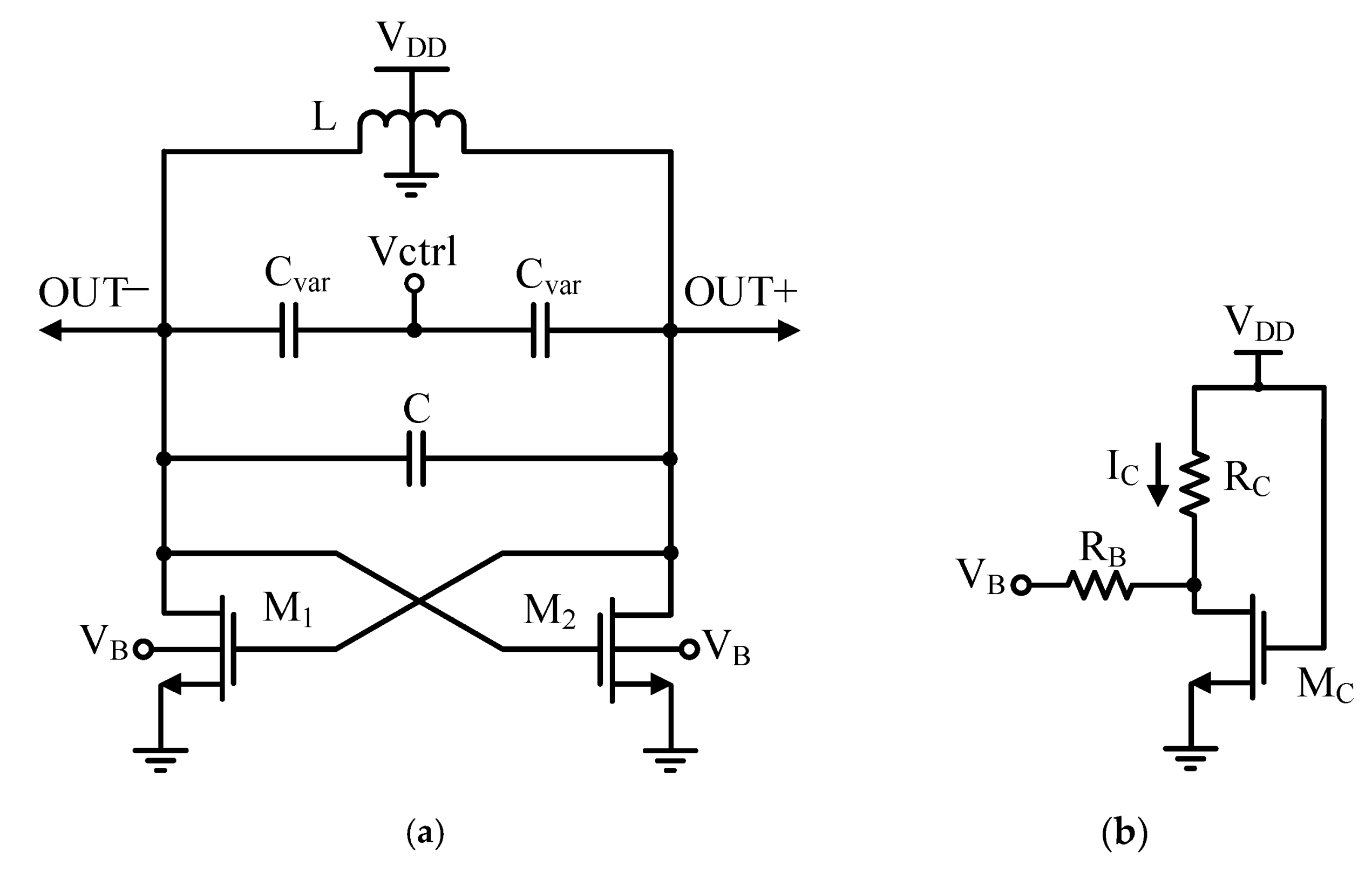
2. Circuit Design
2.1. Proposed Low-Voltage VCO Design
2.2. Analytical Equations
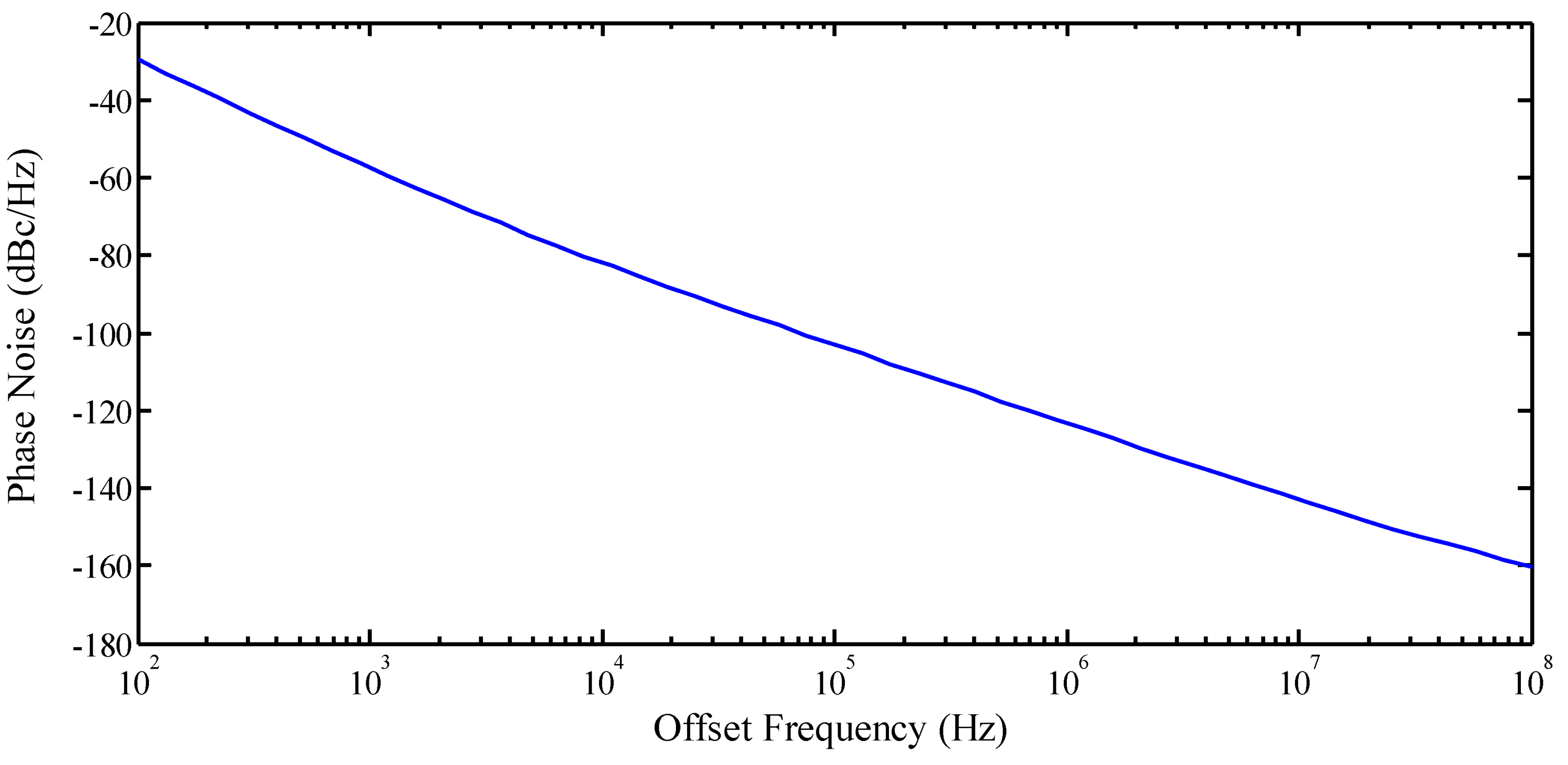
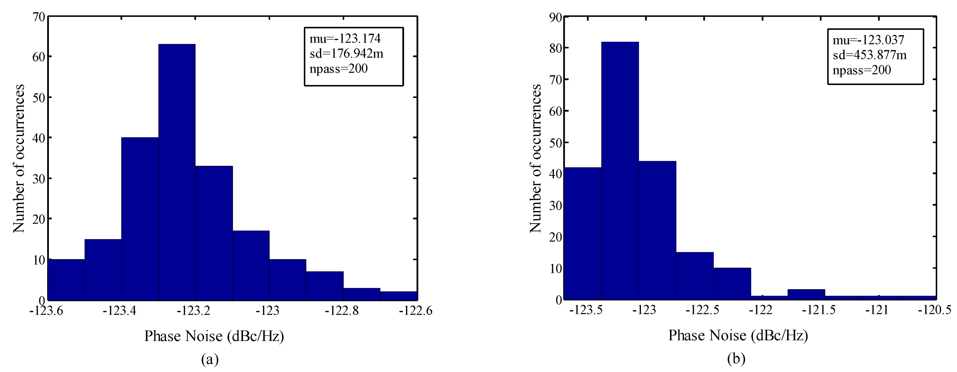
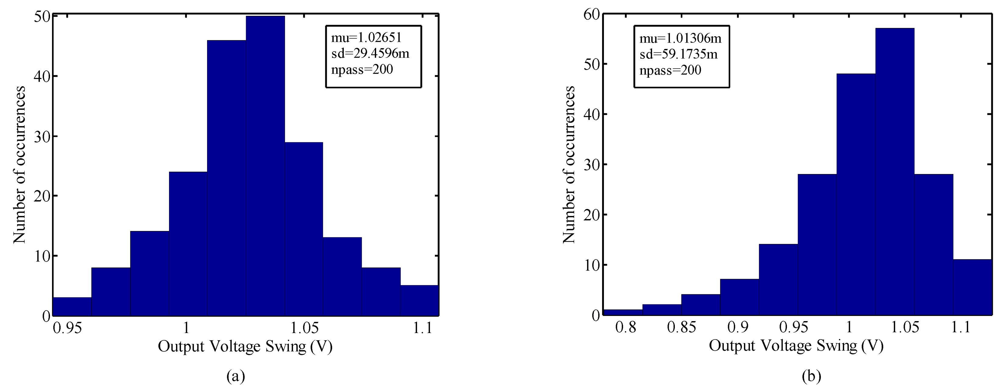
3. Post-Layout Simulation Results
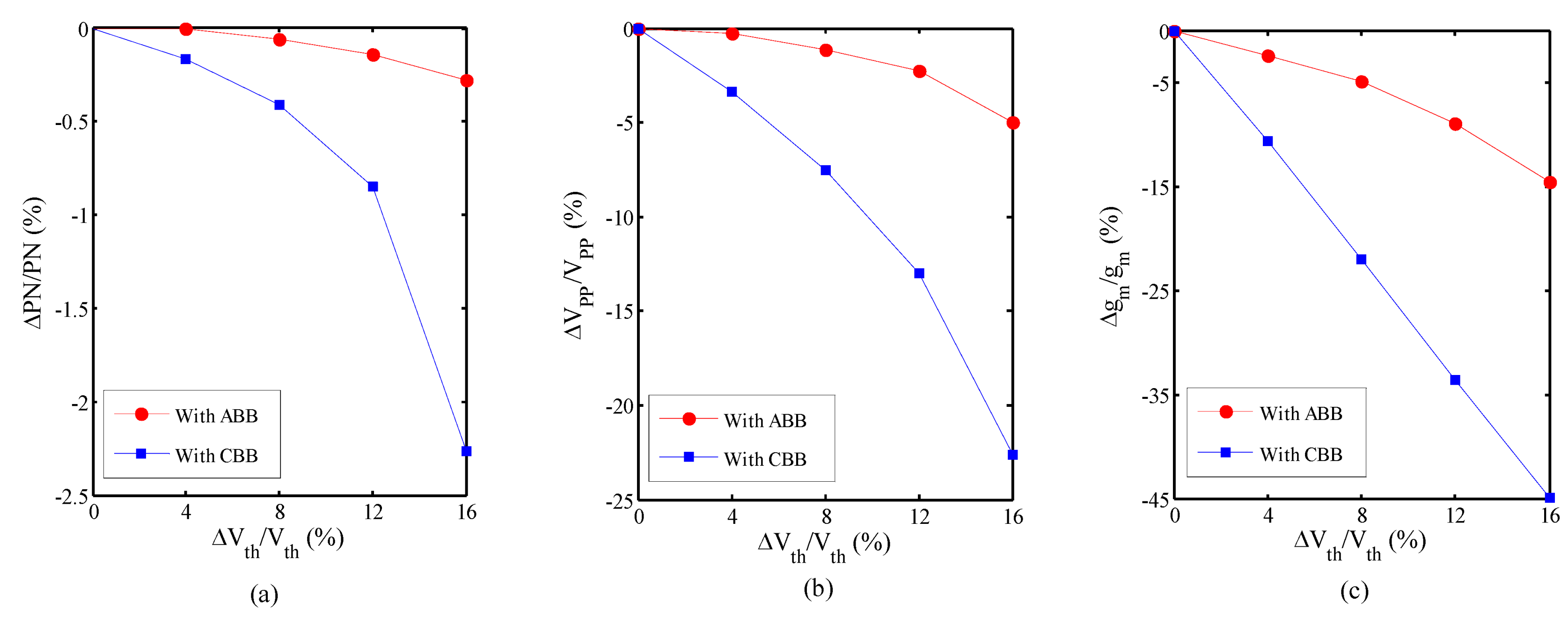
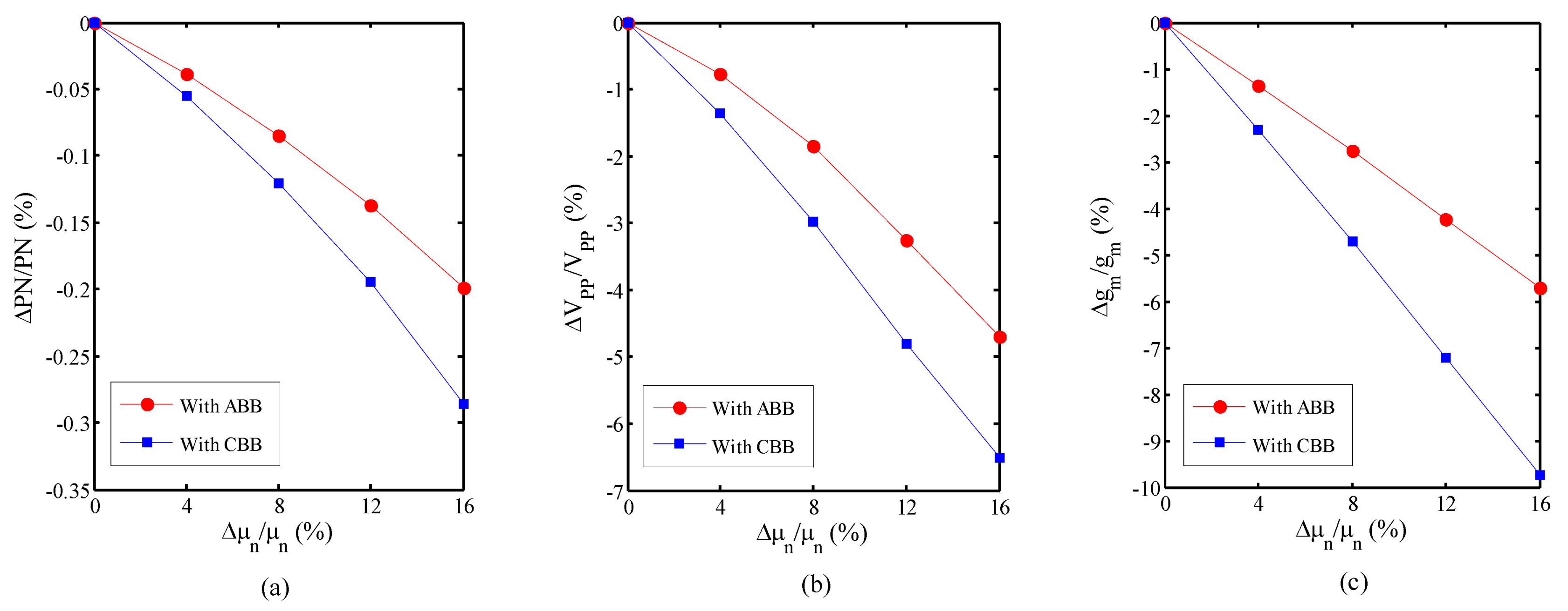
4. Post-Fabrication Practical Consideration
5. Conclusions
Author Contributions
Funding
Data Availability Statement
Conflicts of Interest
References
- Reddy, B., Jr.; Hassan, U.; Seymour, C.; Angus, D.C.; Isbell, T.S.; White, K.; Weir, W.; Yeh, L.; Vincent, A.; Bashir, R. Point-of-care sensors for the management of sepsis. Nat. Biomed. Eng. 2018, 2, 640–648. [Google Scholar] [CrossRef]
- John, A.S.; Price, C.P. Existing and emerging technologies for point-of-care testing. Clin. Biochem. Rev. 2014, 35, 155. [Google Scholar]
- Deng, W.; Wang, L.; Song, S.; Zuo, X. Biosensors in POCT application. Prog. Chem. 2016, 28, 1341. [Google Scholar]
- Rusling, J.F.; Kumar, C.V.; Gutkind, J.S.; Patel, V. Measurement of biomarker proteins for point-of-care early detection and monitoring of cancer. Analyst 2010, 135, 2496–2511. [Google Scholar] [CrossRef] [PubMed]
- Baryeh, K.; Takalkar, S.; Lund, M.; Liu, G. Medical Biosensors for Point of Care (POC) Applications; Elsevier: Amsterdam, The Netherlands, 2017. [Google Scholar]
- Chen, Y.T.; Lee, Y.C.; Lai, Y.H.; Lim, J.C.; Huang, N.T.; Lin, C.T.; Huang, J.J. Review of integrated optical biosensors for point-of-care applications. Biosensors 2020, 10, 209. [Google Scholar] [CrossRef]
- Wang, H. Integrated biosensors in CMOS. In Proceedings of the 2011 IEEE 54th International Midwest Symposium on Circuits and Systems (MWSCAS), Seoul, Republic of Korea, 7–10 August 2011; pp. 1–4. [Google Scholar]
- Singh, R.; Manickam, A.; Hassibi, A. CMOS biochips for hypothesis-driven DNA analysis. In Proceedings of the 2014 IEEE Biomedical Circuits and Systems Conference (BioCAS) Proceedings, Lausanne, Switzerland, 22–24 October 2014; pp. 484–487. [Google Scholar]
- Jang, B.; Hassibi, A. Biosensor systems in standard CMOS processes: Fact or fiction? IEEE Trans. Ind. Electron. 2009, 56, 979–985. [Google Scholar] [CrossRef]
- Ghafar-Zadeh, E.; Sawan, M.; Chodavarapu, V.P.; Hosseini-Nia, T. Bacteria growth monitoring through a differential CMOS capacitive sensor. IEEE Trans. Biomed. Circuits Syst. 2010, 4, 232–238. [Google Scholar] [CrossRef] [PubMed]
- Couniot, N.; Francis, L.A.; Flandre, D. A 16×__16 CMOS capacitive biosensor array towards detection of single bacterial cell. IEEE Trans. Biomed. Circuits Syst. 2015, 10, 364–374. [Google Scholar] [CrossRef]
- Senevirathna, B.P.; Lu, S.; Dandin, M.P.; Basile, J.; Smela, E.; Abshire, P.A. Real-time measurements of cell proliferation using a lab-on-CMOS capacitance sensor array. IEEE Trans. Biomed. Circuits Syst. 2018, 12, 510–520. [Google Scholar] [CrossRef]
- Tabrizi, H.O.; Farhanieh, O.; Owen, Q.; Magierowski, S.; Ghafar-Zadeh, E. Wide input dynamic range fully integrated capacitive sensor for life science applications. IEEE Trans. Biomed. Circuits Syst. 2021, 15, 339–350. [Google Scholar] [CrossRef]
- Tabrizi, H.O.; Forouhi, S.; Ghafar-Zadeh, E. A High Dynamic Range Dual 8× 16 Capacitive Sensor Array for Life Science Applications. IEEE Trans. Biomed. Circuits Syst. 2022, 16, 1191–1203. [Google Scholar] [CrossRef]
- Manickam, A.; Singh, R.; McDermott, M.W.; Wood, N.; Bolouki, S.; Naraghi-Arani, P.; Johnson, K.A.; Kuimelis, R.G.; Schoolnik, G.; Hassibi, A. A fully integrated CMOS fluorescence biochip for DNA and RNA testing. IEEE J. Solid-State Circuits 2017, 52, 2857–2870. [Google Scholar] [CrossRef]
- Adamopoulos, C.; Zarkos, P.; Buchbinder, S.; Bhargava, P.; Niknejad, A.; Anwar, M.; Stojanović, V. Lab-on-Chip for Everyone: Introducing an Electronic-Photonic Platform for Multiparametric Biosensing Using Standard CMOS Processes. IEEE Open J. Solid-State Circuits Soc. 2021, 1, 198–208. [Google Scholar] [CrossRef]
- Hong, L.; Li, H.; Yang, H.; Sengupta, K. Integrated angle-insensitive nanoplasmonic filters for ultraminiaturized fluorescence microarray in a 65 nm digital CMOS process. ACS Photonics 2018, 5, 4312–4322. [Google Scholar] [CrossRef]
- Hong, L.; Li, H.; Yang, H.; Sengupta, K. Fully integrated fluorescence biosensors on-chip employing multi-functional nanoplasmonic optical structures in CMOS. IEEE J. Solid-State Circuits 2017, 52, 2388–2406. [Google Scholar] [CrossRef]
- Eltoukhy, H.; Salama, K.; El Gamal, A. A 0.18 μm CMOS bioluminescence detection lab-on-chip. IEEE J. Solid-State Circuits 2006, 41, 651–662. [Google Scholar] [CrossRef]
- Sideris, C.; Hajimiri, A. An integrated magnetic spectrometer for multiplexed biosensing. In Proceedings of the 2013 IEEE International Solid-State Circuits Conference Digest of Technical Papers, San Francisco, CA, USA, 17–21 February 2013; pp. 300–301. [Google Scholar]
- Handwerker, J.; Pérez-Rodas, M.; Beyerlein, M.; Vincent, F.; Beck, A.; Freytag, N.; Yu, X.; Pohmann, R.; Anders, J.; Scheffler, K. A CMOS NMR needle for probing brain physiology with high spatial and temporal resolution. Nat. Methods 2020, 17, 64–67. [Google Scholar] [CrossRef]
- Lei, K.M.; Ha, D.; Song, Y.Q.; Westervelt, R.M.; Martins, R.; Mak, P.I.; Ham, D. Portable NMR with parallelism. Anal. Chem. 2020, 92, 2112–2120. [Google Scholar] [CrossRef]
- Dreyer, F.; Yang, Q.; Krüger, D.; Anders, J. A chip-based NMR relaxometry system for point-of-care analysis. In Proceedings of the 2022 IEEE Biomedical Circuits and Systems Conference (BioCAS), Taiwan, China, 13–15 October 2022; pp. 183–187. [Google Scholar]
- Wang, H.; Kosai, S.; Sideris, C.; Hajimiri, A. An ultrasensitive CMOS magnetic biosensor array with correlated double counting noise suppression. In Proceedings of the 2010 IEEE MTT-S International Microwave Symposium, Anaheim, CA, USA, 23–28 May 2010; pp. 616–619. [Google Scholar]
- Pai, A.; Khachaturian, A.; Chapman, S.; Hu, A.; Wang, H.; Hajimiri, A. A handheld magnetic sensing platform for antigen and nucleic acid detection. Analyst 2014, 139, 1403–1411. [Google Scholar] [CrossRef] [PubMed]
- Sideris, C.; Khial, P.P.; Ling, B.; Hajimiri, A. A 0.3 ppm dual-resonance transformer-based drift-cancelling reference-free magnetic sensor for biosensing applications. In Proceedings of the 2018 IEEE International Solid-State Circuits Conference-(ISSCC), San Francisco, CA, USA, 11–15 February 2018; pp. 190–192. [Google Scholar]
- Sun, N.; Yoon, T.J.; Lee, H.; Andress, W.; Demas, V.; Prado, P.; Weissleder, R.; Ham, D. Palm NMR and one-chip NMR. In Proceedings of the 2010 IEEE International Solid-State Circuits Conference-(ISSCC), San Francisco, CA, USA, 7–11 February 2010; pp. 488–489. [Google Scholar]
- Wang, H.; Mahdavi, A.; Tirrell, D.A.; Hajimiri, A. A magnetic cell-based sensor. Lab. Chip 2012, 12, 4465–4471. [Google Scholar] [CrossRef]
- Wang, H.; Sideris, C.; Hajimiri, A. A frequency-shift based CMOS magnetic biosensor with spatially uniform sensor transducer gain. In Proceedings of the IEEE Custom Integrated Circuits Conference 2010, San Jose, CA, USA, 19–22 September 2010; pp. 1–4. [Google Scholar]
- Lei, K.-M.; Mak, P.-I.; Law, M.-K.; Martins, R.P. A μNMR CMOS Transceiver Using a Butterfly-Coil Input for Integration with a Digital Microfluidic Device Inside a Portable Magnet. IEEE J. Solid-State Circuits 2016, 51, 2274–2286. [Google Scholar] [CrossRef]
- Wang, H.; Chen, Y.; Hassibi, A.; Scherer, A.; Hajimiri, A. A frequency-shift CMOS magnetic biosensor array with single-bead sensitivity and no external magnet. In Proceedings of the 2009 IEEE International Solid-State Circuits Conference-Digest of Technical Papers, San Francisco, CA, USA, 8–12 February 2009; pp. 438–439. [Google Scholar]
- Chalklen, T.; Jing, Q.; Kar-Narayan, S. Biosensors based on mechanical and electrical detection techniques. Sensors 2020, 20, 5605. [Google Scholar] [CrossRef]
- Arlett, J.L.; Myers, E.B.; Roukes, M.L. Comparative advantages of mechanical biosensors. Nat. Nanotechnol. 2011, 6, 203–215. [Google Scholar] [CrossRef] [PubMed]
- Someya, T.; Islam, A.K.M.M.; Sakurai, T.; Takamiya, M. An 11-nW CMOS temperature-to-digital converter utilizing sub-threshold current at sub-thermal drain voltage. IEEE J. Solid-State Circuits 2019, 54, 613–622. [Google Scholar] [CrossRef]
- Azcona, C.; Calvo, B.; Medrano, N.; Celma, S. 1.2 V–0.18 μm CMOS Temperature Sensors With Quasi-Digital Output for Portable Systems. IEEE Trans. Instrum. Meas. 2015, 64, 2565–2573. [Google Scholar] [CrossRef]
- Pan, S.; Angevare, J.A.; Makinwa, K.A.A. 5.4 A Hybrid Thermal-Diffusivity/Resistor-Based Temperature Sensor with a Self-Calibrated Inaccuracy of±0.25 °C (3 Σ) from −55 °C to 125 °C. In Proceedings of the 2021 IEEE International Solid-State Circuits Conference (ISSCC), San Francisco, CA, USA, 13–22 February 2021; pp. 78–80. [Google Scholar]
- Pan, S.; Makinwa, K.A.A. A 0.25 mm 2-Resistor-Based Temperature Sensor With an Inaccuracy of 0.12 °C (3$\sigma $) From −55 °C to 125 °C. IEEE J. Solid-State Circuits 2018, 53, 3347–3355. [Google Scholar] [CrossRef]
- Rabi, I.I.; Zacharias, J.R.; Millman, S.; Kusch, P. A new method of measuring nuclear magnetic moment. Phys. Rev. 1938, 53, 318. [Google Scholar] [CrossRef]
- Helmy, A.A.; Jeon, H.J.; Lo, Y.C.; Larsson, A.J.; Kulkarni, R.; Kim, J.; Silva-Martinez, J.; Entesari, K. A self-sustained CMOS microwave chemical sensor using a frequency synthesizer. IEEE J. Solid-State Circuits 2012, 47, 2467–2483. [Google Scholar] [CrossRef]
- Nehring, J.; Bartels, M.; Weigel, R.; Kissinger, D. A permittivity sensitive PLL based on a silicon-integrated capacitive sensor for microwave biosensing applications. In Proceedings of the 2015 IEEE Topical Conference on Biomedical Wireless Technologies, Networks, and Sensing Systems (BioWireleSS), San Diego, CA, USA, 25–28 January 2015; pp. 1–3. [Google Scholar]
- Elhadidy, O.; Elkholy, M.; Helmy, A.A.; Palermo, S.; Entesari, K. A CMOS fractional-N PLL-based microwave chemical sensor with 1.5% permittivity accuracy. IEEE Trans. Microw. Theory Tech. 2013, 61, 3402–3416. [Google Scholar] [CrossRef]
- Abdelhalim, K.; Kokarovtseva, L.; Velazquez, J.L.P.; Genov, R. 915-MHz FSK/OOK wireless neural recording SoC with 64 mixed-signal FIR filters. IEEE J. Solid-State Circuits 2013, 48, 2478–2493. [Google Scholar] [CrossRef]
- Lee, M.C.; Karimi-Bidhendi, A.; Malekzadeh-Arasteh, O.; Wang, P.T.; Do, A.H.; Nenadic, Z.; Heydari, P. A CMOS MedRadio Transceiver With Supply-Modulated Power Saving Technique for an Implantable Brain–Machine Interface System. IEEE J. Solid-State Circuits 2019, 54, 1541–1552. [Google Scholar] [CrossRef]
- Chuo, L.X.; Shi, Y.; Luo, Z.; Chiotellis, N.; Foo, Z.; Kim, G.; Kim, Y.; Grbic, A.; Wentzloff, D.; Kim, H.S.; et al. 7.4 A 915MHz asymmetric radio using Q-enhanced amplifier for a fully integrated 3 × 3 × 3 mm 3 wireless sensor node with 20 m non-line-of-sight communication. In Proceedings of the 2017 IEEE International Solid-State Circuits Conference (ISSCC), San Francisco, CA, USA, 5–9 February 2017; pp. 132–133. [Google Scholar]
- Harrison, R.R.; Kier, R.J.; Chestek, C.A.; Gilja, V.; Nuyujukian, P.; Ryu, S.; Greger, B.; Solzbacher, F.; Shenoy, K.V. Wireless neural recording with single low-power integrated circuit. IEEE Trans. Neural Syst. Rehabil. Eng. 2009, 17, 322–329. [Google Scholar] [CrossRef] [PubMed]
- Lee, S.B.; Lee, H.-M.; Kiani, M.; Jow, U.-M.; Ghovanloo, M. An inductively powered scalable 32-channel wireless neural recording system-on-a-chip for neuroscience applications. IEEE Trans. Biomed. Circuits Syst. 2010, 4, 360–371. [Google Scholar]
- Irazoqui-Pastor, P.; Mody, I.; Judy, J.W. In-vivo EEG recording using a wireless implantable neural transceiver. In Proceedings of the First International IEEE EMBS Conference on Neural Engineering, Capri, Italy, 20–22 March 2003; pp. 622–625. [Google Scholar]
- Bernstein, J.B.; Gurfinkel, M.; Li, X.; Walters, J.; Shapira, Y.; Talmor, M. Electronic circuit reliability modeling. Microelectron. Reliab. 2006, 46, 1957–1979. [Google Scholar] [CrossRef]
- Kumar, A.; Ning, T.H.; Fischetti, M.V.; Gusev, E. Hot-carrier charge trapping and reliability in high-k dielectrics. In Proceedings of the 2002 Symposium on VLSI Technology. Digest of Technical Papers (Cat. No.01CH37303), Honolulu, HI, USA, 11–13 June 2002; pp. 2–3. [Google Scholar] [CrossRef]
- Zafar, S.; Kumar, A.; Gusev, E.; Cartier, E. Threshold voltage instabilities in high-k gate dielectric stacks. IEEE Trans. Device Mater. Reliab. 2005, 5, 45–64. [Google Scholar] [CrossRef]
- Tahanout, C.; Tahi, H.; Nadji, B.; Hocini, L. Simple and fast simulation approach to investigate the NBTI effect on suspended gate MOS devices. Int. J. Electron. Lett. 2019, 8, 355–369. [Google Scholar] [CrossRef]
- Mark, W. Scaled CMOS Technology Reliability Users Guide; Jet Propulsion Laboratory, National Aeronautics and Space Administration: Pasadena, CA, USA, 2010. [Google Scholar]
- Afacan, E.; Yelten, M.B.; Dündar, G. Analog design methodologies for reliability in nanoscale CMOS circuits. In Proceedings of the 2017 14th International Conference on Synthesis, Modeling, Analysis and Simulation Methods and Applications to Circuit Design (SMACD), Giardini Naxos, Italy, 12–15 June 2017; pp. 1–4. [Google Scholar]
- Kerber, A.; Nigam, T. Bias temperature instability in scaled CMOS technologies: A circuit perspective. Microelectron. Reliab. 2018, 81, 31–40. [Google Scholar] [CrossRef]
- Parihar, N.; Southwick, R.G.; Wang, M.; Stathis, J.H.; Mahapatra, S. Modeling of NBTI kinetics in replacement metal gate Si and SiGe FinFETs—Part-II: AC stress and recovery. IEEE Trans. Electron. Devices 2018, 65, 1707–1713. [Google Scholar] [CrossRef]
- Chen, M.-J.; Ho, J.-S.; Huang, T.-H.; Yang, C.-H.; Jou, Y.-N.; Wu, T. Back-gate forward bias method for low-voltage CMOS digital circuits. IEEE Trans. Electron. Devices 1996, 43, 904–910. [Google Scholar] [CrossRef]
- Kumar, S.; Handa, M.; Bhasin, H.; Kanaujia, B.K.; Dwari, S.; Gautam, A.K. Optimized Threshold Voltage Variation for Tunable Body Biasing CMOS Power Amplifier. Wirel. Pers. Commun. 2016, 91, 439–452. [Google Scholar] [CrossRef]
- Yuan, J.S.; Chen, S. Power amplifier resilient design for process and temperature variations using an on-chip PLL sensing signal. Microelectron. Reliab. 2014, 54, 167–171. [Google Scholar] [CrossRef]
- Yuan, J.S.; Tang, H. CMOS RF design for reliability using adaptive gate–source biasing. IEEE Trans. Electron. Devices 2008, 55, 2348–2353. [Google Scholar] [CrossRef]
- Liu, Y.; Yuan, J.-S. CMOS RF low-noise amplifier design for variability and reliability. IEEE Trans. Device Mater. Reliab. 2011, 11, 450–457. [Google Scholar] [CrossRef]
- Liu, Y.; Yuan, J.-S. CMOS RF power amplifier variability and reliability resilient biasing design and analysis. IEEE Trans. Electron. Devices 2011, 58, 540–546. [Google Scholar] [CrossRef]
- Liu, Y. Reliability analysis of MOS varactor in CMOS LC VCO. Microelectron. J. 2011, 42, 330–333. [Google Scholar] [CrossRef]
- Hajimiri, A.; Lee, T.H. Design issues in CMOS differential LC oscillators. IEEE J. Solid-State Circuits 1999, 34, 717–724. [Google Scholar] [CrossRef]
- Lee, T.H.; Hajimiri, A. Oscillator phase noise: A tutorial. IEEE J. Solid-State Circuits 2000, 35, 326–336. [Google Scholar] [CrossRef]
- Cheng, K.-W.; Chang, S.-K.; Huang, Y.-C. Low-Power and Low-Phase-Noise Gm-Enhanced Current-Reuse Differential Colpitts VCO. IEEE Trans. Circuits Syst. II Express Briefs 2019, 66, 733–737. [Google Scholar]
- Azadmousavi, T.; Aghdam, E.N. A Low Power Current-Reuse LC-VCO with an Adaptive Body-Biasing Technique. AEU-Int. J. Electron. Commun. 2018, 89, 56–61. [Google Scholar] [CrossRef]
- Amer, A.G.; Ibrahim, S.A.; Ragai, H.F. A 1-mW 12-GHz LC VCO in 65-nm CMOS technology. In Proceedings of the 2016 IEEE International Conference on Electronics, Circuits and Systems, ICECS 2016, Monte Carlo, Monaco, 11–14 December 2016; pp. 456–459. [Google Scholar] [CrossRef]
- Jafari, B.; Sheikhaei, S. Low phase noise LC VCO with sinusoidal tail current shaping using cascode current source. AEU-Int. J. Electron. Commun. 2018, 83, 114–122. [Google Scholar] [CrossRef]
- Razavi, B. RF Microelectronics, 2nd ed.; Prentice Hall: Hoboken, NJ, USA, 2011. [Google Scholar]
- Razavi, B. Design of Analog CMOS Integrated Circuits; McGraw-Hill: Boston, MA, USA, 2001. [Google Scholar]
- Li, M.; Seok, S.; Rolland, N.; Rolland, P.-A. Design, realization and test of a 2.1 GHz ultra-low phase noise oscillator based on BAW resonator. AEU-Int. J. Electron. Commun. 2011, 65, 602–607. [Google Scholar] [CrossRef]
- Sadr, H.R.; Dousti, M. Purification of inductors and improvement of phase noise in monolithic differential LC-VCOs. AEU-Int. J. Electron. Commun. 2012, 66, 128–132. [Google Scholar] [CrossRef]
- Hajimiri, A.; Lee, T.H. A general theory of phase noise in electrical oscillators. IEEE J. Solid-State Circuits 1998, 33, 179–194. [Google Scholar] [CrossRef]
- Kebe, M.; Sanduleanu, M. A Low-Phase-Noise 8 GHz Linear-Band Sub-Millimeter-Wave Phase-Locked Loop in 22 nm FD-SOI CMOS. Micromachines 2023, 14, 1010. [Google Scholar] [CrossRef]
- Chee, Y.H.; Rabaey, J.M.; Niknejad, A. Ultra Low Power Transmitters for Wireless Sensor Networks. Ph.D. Thesis, University of California, Berkeley, CA, USA, 2006. [Google Scholar]
- Lavrič, A.; Batagelj, B.; Vidmar, M. Calibration of an RF/Microwave Phase Noise Meter with a Photonic Delay Line. Photonics 2022, 9, 533. [Google Scholar] [CrossRef]
- Yun, S.-J.; Shin, S.-B.; Choi, H.-C.; Lee, S.-G. A 1mW current-reuse CMOS differential LC-VCO with low phase noise. In Proceedings of the Solid-State Circuits Conference, San Francisco, CA, USA, 10 February 2005; pp. 540–616. [Google Scholar]
- Naseh, S.; Dooghabadi, M.Z.; Deen, M.J. A low-voltage low-noise superharmonic quadrature oscillator. In Proceedings of the 2008 15th IEEE International Conference on Electronics, Circuits and Systems, Malta, Italy, 31 August–3 September 2008; pp. 400–403. [Google Scholar]
- Ying, W.; Qin, P.; Jin, J.; Mo, T. A 1mW 5GHz current reuse CMOS VCO with low phase noise and balanced differential outputs. In Proceedings of the 2011 International Symposium on Integrated Circuits, Singapore, 12–14 December 2011; pp. 543–546. [Google Scholar]
- Hsu, M.-T.; Li, W.-J.; Hsu, S.-C. Design of low phase noise CMOS VCO using cross coupled topology with capacitor feedback. Microelectron. J. 2016, 54, 32–39. [Google Scholar] [CrossRef]


| Parameters | Values | Parameters | Values |
|---|---|---|---|
| WM1/LM1 | 6 × 2 µm/0.18 µm | L | 9.46 nH |
| WM1/LM1 | 6 × 2 µm/0.18 µm | RB | 20 kΩ |
| WMC/LMC | 1.5 µm/0.18 µm | RC | 25 kΩ |
| C | 190 fF |
| Corners | a SS | b FF | c FS | d SF |
|---|---|---|---|---|
| Phase Noise (dBc/Hz) | −122.1 | −123.18 | −123.55 | −122.83 |
| FoM (dBc/Hz) | −193.52 | −193.37 | −193.63 | −194.65 |
| Work | a [65] | b [68] | b [78] | b [79] | b [80] | b This Work |
|---|---|---|---|---|---|---|
| CMOS Process (nm) | 180 | 180 | 180 | 180 | 180 | 180 |
| Power Supply (V) | 1.1 | 1.8 | 1 | 1.2 | 0.8 | 0.6 |
| Power consumption (mW) | 1.4 | 1 | c 3 | 1 | 3.14 | 0.398 |
| Oscillation Frequency (GHz) | 2.4 | 4 | 5 | 5 | 5.4 | 2.4 |
| Phase Noise (dBc/Hz) @ 1 MHz | −122.85 | −116.8 | −108 | −117.7 | −119.5 | −123.19 |
| FoM (dBc/Hz) | −189 | −188.9 | −177.21 | −191.8 | −189.18 | −194.82 |
Disclaimer/Publisher’s Note: The statements, opinions and data contained in all publications are solely those of the individual author(s) and contributor(s) and not of MDPI and/or the editor(s). MDPI and/or the editor(s) disclaim responsibility for any injury to people or property resulting from any ideas, methods, instructions or products referred to in the content. |
© 2023 by the authors. Licensee MDPI, Basel, Switzerland. This article is an open access article distributed under the terms and conditions of the Creative Commons Attribution (CC BY) license (https://creativecommons.org/licenses/by/4.0/).
Share and Cite
Azadmousavi, T.; Ghafar-Zadeh, E. Design and Analysis of a Low-Voltage VCO: Reliability and Variability Performance. Micromachines 2023, 14, 2118. https://doi.org/10.3390/mi14112118
Azadmousavi T, Ghafar-Zadeh E. Design and Analysis of a Low-Voltage VCO: Reliability and Variability Performance. Micromachines. 2023; 14(11):2118. https://doi.org/10.3390/mi14112118
Chicago/Turabian StyleAzadmousavi, Tayebeh, and Ebrahim Ghafar-Zadeh. 2023. "Design and Analysis of a Low-Voltage VCO: Reliability and Variability Performance" Micromachines 14, no. 11: 2118. https://doi.org/10.3390/mi14112118
APA StyleAzadmousavi, T., & Ghafar-Zadeh, E. (2023). Design and Analysis of a Low-Voltage VCO: Reliability and Variability Performance. Micromachines, 14(11), 2118. https://doi.org/10.3390/mi14112118