Article

Compact Integration of Hydrogen–Resistant a–InGaZnO and Poly–Si Thin–Film Transistors

1
School of Electronic and Computer Engineering, Peking University, Shenzhen 518055, China
2
State Key Laboratory of Advanced Displays and Optoelectronics and Technologies, Department of Electronic & Computer Engineering, The Hong Kong University of Science and Technology, Hong Kong 999077, China
3
College of Electronic and Information Engineering, Shenzhen University, Shenzhen 518060, China
*
Author to whom correspondence should be addressed.
Micromachines 2022, 13(6), 839; https://doi.org/10.3390/mi13060839
Submission received: 6 May 2022 / Revised: 17 May 2022 / Accepted: 21 May 2022 / Published: 27 May 2022
(This article belongs to the Special Issue Recent Advances in Thin Film Transistors)

Abstract

:
The low–temperature poly–Si oxide (LTPO) backplane is realized by monolithically integrating low–temperature poly–Si (LTPS) and amorphous oxide semiconductor (AOS) thin–film transistors (TFTs) in the same display backplane. The LTPO–enabled dynamic refreshing rate can significantly reduce the display’s power consumption. However, the essential hydrogenation of LTPS would seriously deteriorate AOS TFTs by increasing the population of channel defects and carriers. Hydrogen (H) diffusion barriers were comparatively investigated to reduce the H content in amorphous indium–gallium–zinc oxide (a–IGZO). Moreover, the intrinsic H–resistance of a–IGZO was impressively enhanced by plasma treatments, such as fluorine and nitrous oxide. Enabled by the suppressed H conflict, a novel AOS/LTPS integration structure was tested by directly stacking the H–resistant a–IGZO on poly–Si TFT, dubbed metal–oxide–on–Si (MOOS). The noticeably shrunken layout footprint could support much higher resolution and pixel density for next–generation displays, especially AR and VR displays. Compared to the conventional LTPO circuits, the more compact MOOS circuits exhibited similar characteristics.

1. Introduction

As the amorphous silicon thin–film transistors (TFTs) cannot meet the elevated requirements of active–matrix displays on higher resolution, the lower power consumption, and higher flexibility, the low–temperature fabrication, the ultralow off–state current (Ioff), and other superiorities of AOS TFTs [1,2] have attracted attention in the rapidly growing field of research in in display [3] and flexible electronics [4]. The amorphous indium–gallium–zinc oxide (a–IGZO) TFT [5] is evidence of progress in this field. However, AOS TFTs exhibited relatively lower mobility and poorer stability compared to low–temperature poly–Si (LTPS) TFTs, restricting their applications to high–end displays and other cutting–edge electronic systems. To combine the metrics of both LTPS and AOS, the low–temperature poly–Si oxide (LTPO) technology was tested by monolithically integrating LTPS and AOS TFTs. This technology enables a dynamic refresh rate and, thus, considerably reduces power consumption [6]. Unfortunately, as the hydrogen (H) doping is essential for passivating the dangling bonds in LTPS [7], the AOS TFTs would be severely degraded by these H dopants diffused from the LTPS TFTs, due to the abundant generation of defects and donors in the AOS channels [8]. Thus, it is imperative for the further improvement of LTPO systems to suppress the detrimental H–influence on AOS TFTs [9,10].
Although metal films have strong H–blocking capabilities [11], they are not suitable for the hybrid integration structures due to potential problems, such as a short circuit. Previous studies proved that the atomic–layer–deposited (ALD) alumina (AlOX) was able to weaken H penetration [12,13,14,15,16]. However, the ALD process itself is rich in H and unsuited to large–area applications. The more compatible H–blocking layer was studied in this work. Furthermore, the H–resistant capability of the AOS channel needs fundamental enhancements. The fluorine (F) plasma treatment has been demonstrated to effectively suppress oxygen–related native defects and enhances the H–resilience of a–IGZO [11,14,17]. Given the corrosive effect of F on common dielectrics, a more moderate pretreatment was developed to realize the H–resistant AOS. Given the suppressed H conflict between LTPS and AOS, a more compact integration architecture of LTPO was proposed in this work for developing advanced displays with higher resolutions and pixels per inch (PPI).

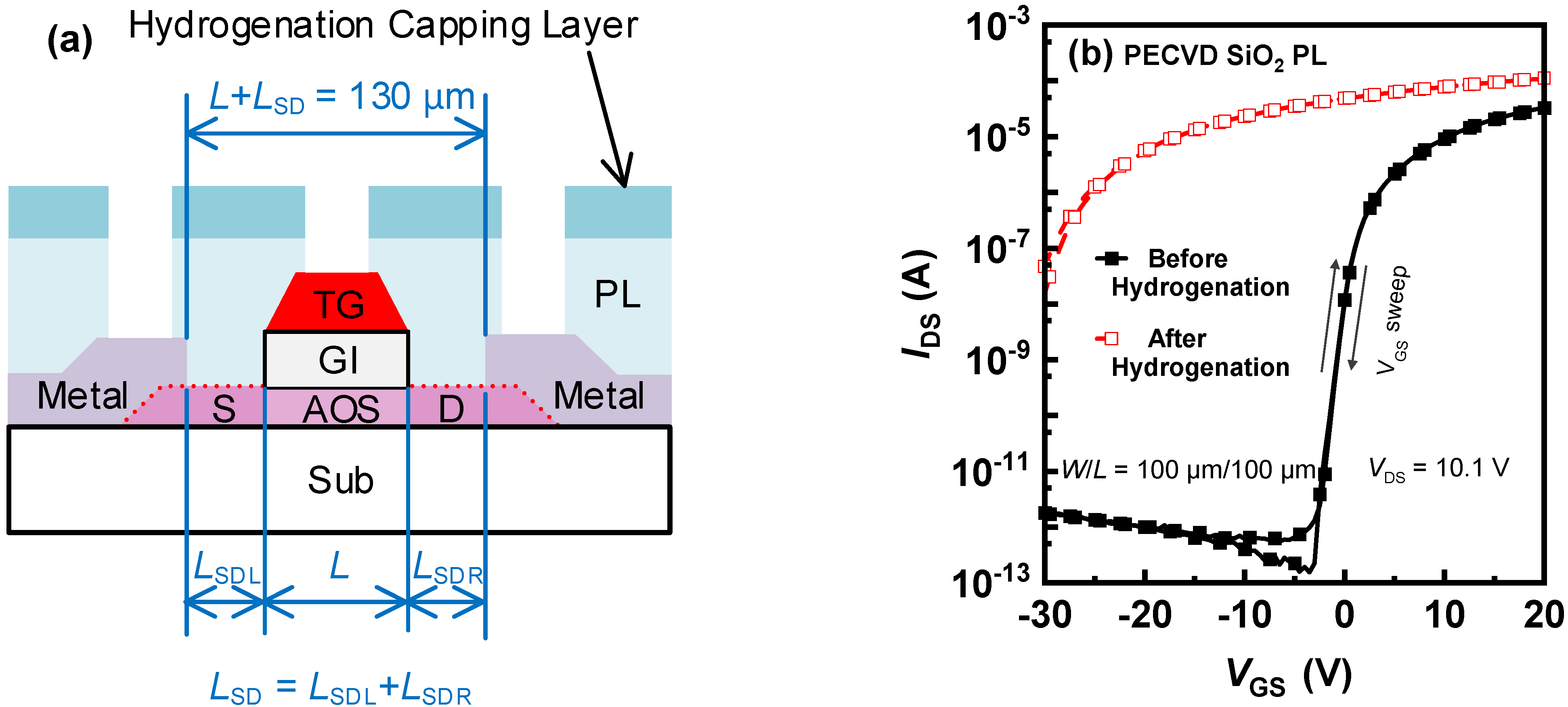
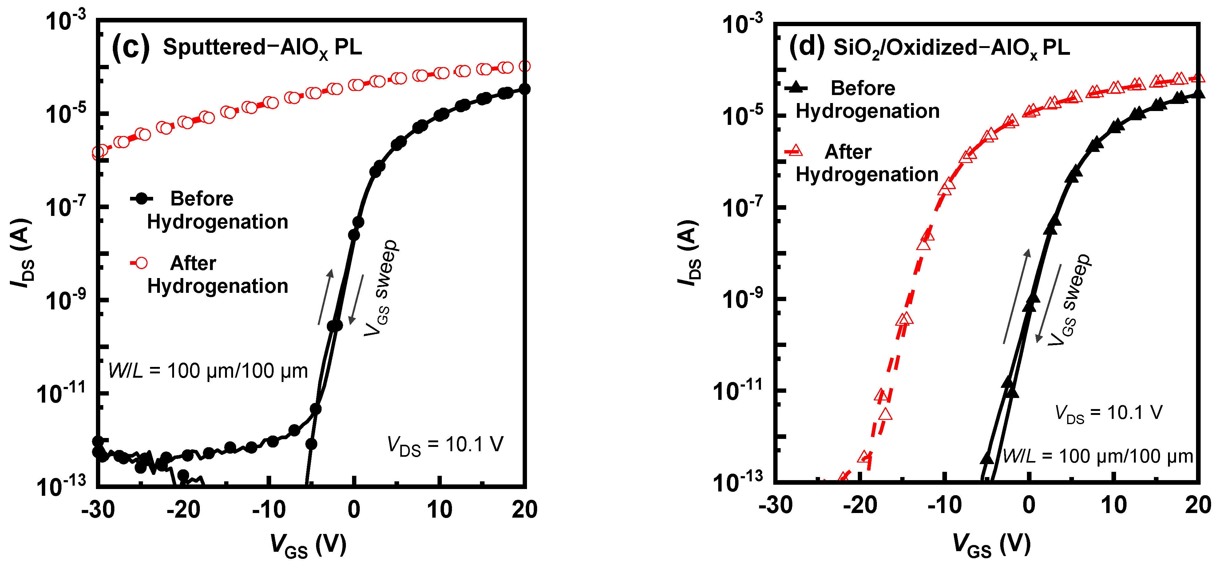
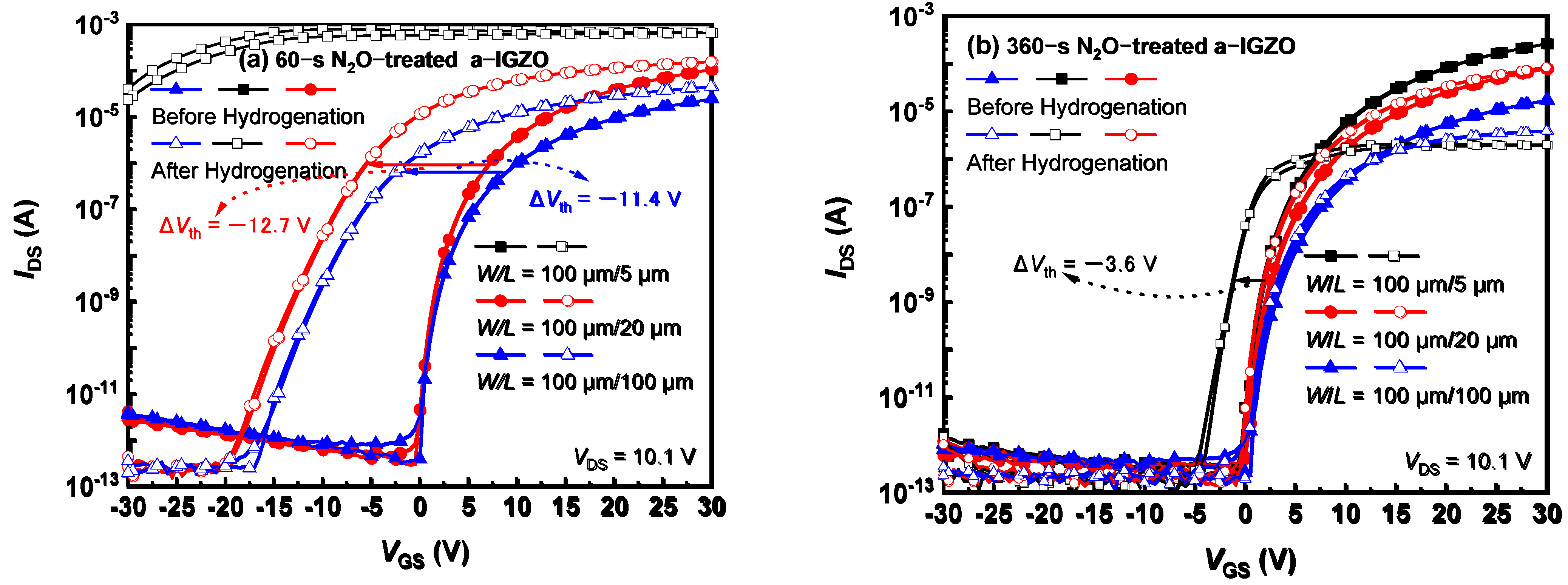
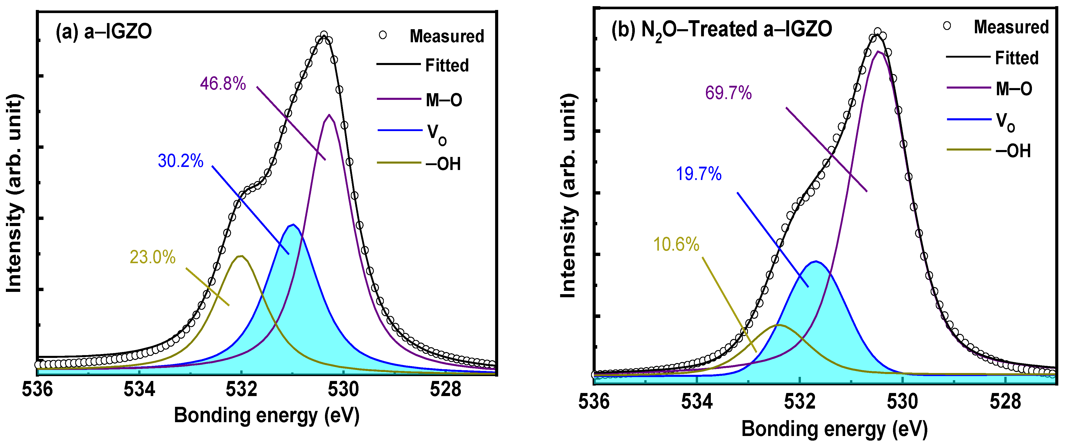
2. Development of Hydrogen–Resistant a–IGZO TFTs

As shown in Figure 1a, the a–IGZO TFTs were fabricated in the self–aligned top–gate (SATG) architecture; this procedure followed our previously reported process [11,14]. The H–blocking capabilities of passivation layers (PL) were compared to different passivation–layer materials. The controlled passivation layer was 200–nm–thick silicon oxide (SiO2) deposited using the plasma–enhanced chemical vapor deposition (PECVD) with silane (SiH4) and nitrous oxide (N2O) as the reactive gases. Another passivation layer of 200–nm–thick AlOX was reactively sputtered in the argon–O2 mixed ambience; the aluminum (Al) target was used for this procedure. On top of the PECVD–SiO2 passivation layer, a 5–nm sputtered Al film was fully oxidized in O2 at 200 °C for 30 s, forming the SiO2/Oxidized–AlOX bilayer. The hydrogenation treatment of these a–IGZO TFTs was implemented by capping these a–IGZO TFTs with H–rich PECVD silicon nitride (SiNX:H) deposited with the SiH4 and ammonia (NH3). These SATG a–IGZO TFTs with a different passivation layer were characterized with the B1500A Semiconductor Parameter Analyzer semiconductor analyzer, before and after the hydrogenation process.
The drain current (IDS) versus gate voltage (VGS) transfer curves of transistors with both a channel width (W) and a length (L) of 100 μm were measured at a drain voltage (VDS) of 10.1 V. The threshold voltage (Vth) was extracted as the VGS corresponding to an L/W-normalized IDS of 10−6 A. In Figure 1b, the Vth of the SiO2–passivated a–IGZO TFT was 0.5 V before the hydrogenation and severely degraded to −28.5 V after the hydrogenation, a result suggesting that abundant H dopants diffuse through the SiO2 passivation layer into a–IGZO channel [18]. The TFTs with a sputtered–AlOX passivation layer were short–circuited by the hydrogenation (Figure 1c), while the extracted Vth of the SiO2/AlOX–passivated TFT only shifted to −11 V (Figure 1d). The results indicated that the film compactness of sputtered AlOX was even worse than that of PECVD SiO2, leading to the heavily H–doped conductive channel. With the addition of only 5–nm thermally–oxidized AlOX, the SiO2/oxidized–AlOX bilayer exhibited much better H–blocking capability than the SiO2 single layer. However, the ultrathin thermally–oxidized AlOX cannot completely block the H diffusion, due to the self–limited nature of Al oxidization. Therefore, it is necessary to elevate the intrinsic H–resistance of AOS TFTs against the residual H dopants penetrating through the bilayer passivation layer.
The H–resistance of SiO2–passivated AOS TFTs was further investigated by additionally treating the a–IGZO islands with N2O plasma at 150 °C. In Figure 2a,b, the H–effects were compared on the a–IGZO TFTs with different N2O treatment times. As shown in Figure 1b, the untreated a–IGZO TFTs were seriously degraded by hydrogenation. The nearly shorted channel is caused by the numerous H dopants that penetrate the SiO2 passivation layer and diffuse into a–IGZO. For the same L of 100 μm, the H–induced ΔVth (Vth before and after the hydrogenation) was significantly decreased to −11.4 V by the 60–s N2O treatment, as shown in Figure 2a. This suggests that the H–resistance of the N2O–treated a–IGZO channel was effectively strengthened. However, the ΔVth of 20–μm–L TFT shifted to −12.7 V, and the 5–μm–L channel was still shorted. Such an apparent short–channel effect (SCE) reveals that the channel–carrier concentration is gradually increased by the lateral H diffusion; this evidence is consistent with the perfect H–blocking capability of the top metal gate [19].
When the N2O treatment was prolonged to 360 s (Figure 2b), the Vth of long–channel TFTs exhibited almost no degradation after the hydrogenation, while the ΔVth of 5–μm–L TFT only slightly shifted to −3.6 V, revealing a significantly strengthened H–resistance of such strongly oxidized a–IGZO. However, the on–state current (Ion) of such strongly oxidized a–IGZO TFT was degraded after the hydrogenation, especially for the 5–μm–L transistor, a result suggesting a significantly increased source/drain (S/D) resistance (RSD). Most plausibly, although the resistivity of strongly oxidized a–IGZO can still be effectively reduced by the argon plasma–induced donor defects [17,20], the additional H dopants suppress these donor defects rather than further supply donors; this process could result in an elevated RSD. As illustrated in Figure 1a, the LSD is even longer for the shorter–L transistor, causing an even larger RSD and thus seriously limiting the Ion of 5–μm–L TFT (Figure 2b).
To analyze the influence of N2O plasma treatment on a–IGZO, the O1s spectra of IGZO were measured by X–ray photoelectron spectroscopy (XPS). The O1s peak consists of three Gaussian subpeaks centered at 532.4 eV, 531.25 eV, and 530.15 eV, respectively corresponding to the hydroxy (–OH) group, oxygen deficiency, and the oxygen bonded with metal cations [21]. As shown in Figure 3, the N2O plasma treatment noticeably suppressed the oxygen deficiency peak in the a–IGZO, while the area percentage of the metal–oxygen (M–O) peak was increased by 22.9%. This result suggests that the N2O treatment effectively annihilates the defects in a–IGZO, such as oxygen vacancy (VO) and –OH. The H dopants in AOS are normally believed to either form –OH groups or occupy the Vo site to form metal-hydrogen (M–H) bonds [21], while the M–H bonds are much more thermally stable than the former [22]. With the Vo defects effectively suppressed by the N2O plasma, the less–defective a–IGZO may obtains certain capability of H–resistance or H–blocking, while the residual H effect can hardly be eliminated by the prolonged oxidization.
The fluorination can also effectively passivate the O– and H–related defects in AOS [23,24]; thus, it was combined with the N2O plasma in this work. The as–deposited a–IGZO was first immersed in the carbon tetrafluoride (CF4) plasma at 150 °C for 600 s to form the fluorinated a–IGZO (a–IGZO:F) and then treated with the N2O plasma for 360 s in the same PECVD reactor. As shown in Figure 4a, the key parameters of N2O–treated a–IGZO:F TFTs were well maintained after the hydrogenation, including the field–effect mobility (μFE), subthreshold slope (SS), and on/off ratio (Figure 4b). Even for 5–μm–L TFT, the ΔVth only slightly degraded by less than −1.5 V. In addition, the RSD after the hydrogenation of a–IGZO is 185.1 kΩ/sq, and a–IGZO:F is 110.0 kΩ/sq, which is reduced by 40%, a reduction that improves the serious degradation of Ion. The metal fluorine (M–F) bonds formed during the fluorination process have much higher dissociation energies than the counterpart M–O bond [25], as listed in the Inset. Therefore, the combination of fluorination and oxidization furthest suppresses the native defects in a–IGZO and thus effectively enhances the H–resistant capability of a–IGZO TFTs.

3. 3D Integration of IGZO and Poly–Si TFTs

The successful development of H–resistant AOS TFT blazes a new trail for LTPO architecture. Distinct from the conventional side–by–side LTPO structure [26], a 3D integration structure of LTPS and a–IGZO TFTs, dubbed metal–oxide–on–Si (MOOS) architecture, was proposed; the demonstration of a basic inverter circuit supported this proposal. The H–resistant a–IGZO:F TFT was also fabricated in the bottom–gate elevated–metal metal–oxide (EMMO) structure [16] and then integrated with the solid–phase–crystallized (SPC) LTPS TFT [27]. The source/drain (S/D) activation of n+ a–IGZO and p+ LTPS was implemented with the same O2 annealing process at 500 °C for 4 h. Distinct from the existing side–by–side LTPO structure [26], a 3D integration structure of LTPS and a–IGZO TFTs was proposed, and this proposal was supported by the demonstration of an inverter circuit module, dubbed metal–oxide–on–Si (MOOS) architecture. As shown in Figure 5a, the CMOS inverter built in the mainstream planar LTPO structure occupies a large footprint and thus cannot meet the increasing demands on high–resolution high–PPI display. The MOOS invertor exhibited a superior layout efficiency by saving nearly 16% area. However, the compact integration of a–IGZO and LTPS TFTs demands a strong H–immunity of IGZO transistor.
In Figure 6a, the full–swing CMOS inverters were successfully demonstrated by integrating the n–type a–IGZO:F TFT and the p–type poly–Si TFT. In light of the process flow of LTPS TFT, only one more photolithography mask of AOS island is added for realizing a compact CMOS circuit, while the traditional CMOS poly–Si circuits require at least two more masks than PMOS poly–Si circuits. Due to the absence of high–performance p–type AOS, the AOS inverters are normally made of unipolar AOS and thus hardly achieve the full swing, or the number of transistors has to be doubled to realize the pseudo–CMOS circuits [28]. The low–cost CMOS circuits can be achieved by hybrid integrating AOS and LTPS, and the integration density can be further enhanced by using the MOOS structure.
The dynamic performance of the traditional LTPO and the proposed MOOS were further compared using the 19–stage ring oscillator. As shown in Figure 6b, both kinds of ring oscillators worked properly, while the oscillating frequency of the MOOS–structure ring oscillator is 184 kHz, slightly smaller than the 201 kHz of the traditional LTPO counterpart. This may originate from the increased capacitance of crossover areas in the more compact MOOS integration structure, which could be improved using a more sophisticated layout design. This indicates that once the influence on AOS of H species from LTPS is considerably suppressed, a 3D integration of AOS and LTPS can be realized, exhibiting great potentials in advanced displays and other cutting–edge applications, such as virtual reality (VR) and augmented reality (AR).

4. Results

In this work, a–IGZO TFTs with different passivation layers were comparatively subjected to hydrogenation, and the results recommended the PECVD SiO2/thermally–oxidized AlOX bilayer as the H–blocking candidate. The combination of N2O pretreatment and fluorine doping was developed to significantly enhance the intrinsic H–resilience of a–IGZO channel by annihilating the native defects. Enabled by the effectively H–resistant AOS TFT, a novel LTPS/AOS integration architecture was tested by stacking the H–resistant IGZO on poly–Si, dubbed metal–oxide–on–Si (MOOS). Comparable electrical characteristics of basic circuits were achieved using both conventional 2D LTPO and 3D MOOS technologies. The significantly reduced layout of the MOOS scheme exhibits a great potential in high–resolution high–PPI displays, especially the next–generation VR/AR/MR displays.

Author Contributions

Conceptualization, M.W. and L.L.; methodology, Y.W. and L.L.; writing—original draft preparation, Y.Z., Z.X., W.Z., Y.W. and L.L.; writing—review and editing, M.Z. and S.Z.; project administration, Y.W. and F.S.Y.Y.; funding acquisition, M.W., H.S.K. and L.L. All authors have read and agreed to the published version of the manuscript.

Funding

This research was funded by Shenzhen Research Programs grant number JCYJ20190808154803565, JCYJ20200109140601691, SGDX20190918105001787, SGDX20201103095607022, SGDX20201103095610029 and GXWD20201231165807007–20200807025846001.

Data Availability Statement

Not applicable.

Conflicts of Interest

The authors declare no conflict of interest.

References

  1. Wang, D.; Furuta, M.; Tomai, S.; Yano, K. Understanding the Role of Temperature and Drain Current Stress in InSnZnO TFTs with Various Active Layer Thicknesses. Nanomaterials 2020, 10, 617. [Google Scholar] [CrossRef] [PubMed] [Green Version]
  2. Wang, D.; Furuta, M.; Tomai, S.; Yano, K. Impact of Photo-Excitation on Leakage Current and Negative Bias Instability in InSnZnO Thickness-Varied Thin-Film Transistors. Nanomaterials 2020, 10, 1782. [Google Scholar] [CrossRef] [PubMed]
  3. Chortos, A.; Zhu, C.; Oh, J.Y.; Yan, X.; Pochorovski, I.; To, J.W.-F.; Liu, N.; Kraft, U.; Murmann, B.; Bao, Z. Investigating Limiting Factors in Stretchable All-Carbon Transistors for Reliable Stretchable Electronics. ACS Nano 2017, 11, 7925–7937. [Google Scholar] [CrossRef] [PubMed]
  4. Magari, Y.; Kataoka, T.; Yeh, W.; Furuta, M. High-mobility hydrogenated polycrystalline In2O3 (In2O3:H) thin-film transistors. Nat. Commun. 2022, 13, 1078. [Google Scholar] [CrossRef]
  5. Um, J.K.; Lee, S.; Jin, S.; Mativenga, M.; Oh, S.Y.; Lee, C.H.; Jang, J. High-Performance Homojunction a-IGZO TFTs With Selectively Defined Low-Resistive a-IGZO Source/Drain Electrodes. IEEE Trans. Electron Devices 2015, 62, 2212–2218. [Google Scholar] [CrossRef]
  6. Chang, S.C.; Hung, M.-C.; Yu, C.-H.; Chang, T.-K.; Roudbari, A.J.; Lin, S.-C.; Kim, K.-W.; Huang, C.-Y.; Lee, S.-H.; Chen, Y.-C. Liquid Crystal Displays with Oxide-Based Thin-Film Tran-sistors. Application No US-0228070, 27 March 2014. [Google Scholar]
  7. Seager, C.H.; Ginley, D.S. Passivation of grain boundaries in polycrystalline silicon. Appl. Phys. Lett. 1979, 34, 337–340. [Google Scholar] [CrossRef]
  8. Bang, J.; Matsuishi, S.; Hosono, H. Hydrogen anion and subgap states in amorphous In–Ga–Zn–O thin films for TFT applications. Appl. Phys. Lett. 2017, 110, 232105. [Google Scholar] [CrossRef] [Green Version]
  9. Abliz, A.; Gao, Q.; Wan, D.; Liu, X.; Xu, L.; Liu, C.; Jiang, C.; Li, X.; Chen, H.; Guo, T.; et al. Effects of Nitrogen and Hydrogen Codoping on the Electrical Performance and Reliability of InGaZnO Thin-Film Transistors. ACS Appl. Mater. Interfaces 2017, 9, 10798–10804. [Google Scholar] [CrossRef]
  10. Abliz, A. Effects of hydrogen plasma treatment on the electrical performances and reliability of InGaZnO thin-film transistors. J. Alloys Compd. 2020, 831, 154694. [Google Scholar] [CrossRef]
  11. Lv, N.; Lu, L.; Wang, Z.; Wang, H.; Zhang, D.; Wong, M.; Wang, M. Suppression of the Short-Channel Effect in Dehydrogenated Elevated-Metal Metal- Oxide (EMMO) Thin-Film Transistors. IEEE Trans. Electron Devices 2020, 67, 3001–3004. [Google Scholar] [CrossRef]
  12. Hanyu, Y.; Domen, K.; Nomura, K.; Hiramatsu, H.; Kumomi, H.; Hosono, H.; Kamiya, T. Hydrogen passivation of electron trap in amorphous In-Ga-Zn-O thin-film transistors. Appl. Phys. Lett. 2013, 103, 202114. [Google Scholar] [CrossRef]
  13. Chowdhury, D.H.; Mativenga, M.; Um, J.G.; Mruthyunjaya, R.K.; Heiler, G.N.; Tredwell, T.J.; Jang, J. Effect of SiO2 and SiO2/SiNx Passivation on the Stability of Amorphous Indium-Gallium Zinc-Oxide Thin-Film Transistors Under High Humidity. IEEE Trans. Electron Devices 2015, 62, 869–874. [Google Scholar] [CrossRef]
  14. Peng, H.; Chang, B.; Fu, H.; Yang, H.; Zhang, Y.; Zhou, X.; Lu, L.; Zhang, S. Top-Gate Amorphous Indium-Gallium-Zinc-OxideThin-Film Transistors with Magnesium Metallized Source/Drain Regions. IEEE Trans. Electron Devices 2020, 67, 1619–1624. [Google Scholar] [CrossRef]
  15. Lu, L.; Li, J.; Feng, Z.Q.; Kwok, H.S.; Wong, M. Elevated-Metal Metal-Oxide (EMMO) Thin-Film Transistor: Technology and Characteristics. IEEE Electron Device Lett. 2016, 37, 728–730. [Google Scholar] [CrossRef]
  16. Wang, S.; Shi, R.; Li, J.; Lu, L.; Xia, Z.; Kwok, H.S.; Wong, M. Resilience of Fluorinated Indium-Gallium-Zinc Oxide Thin-Film Transistor Against Hydrogen-Induced Degradation. IEEE Electron Device Lett. 2020, 41, 729–732. [Google Scholar] [CrossRef]
  17. Wang, S.; Li, J.; Shi, R.; Xia, Z.; Lu, L.; Kwok, H.S.; Wong, M. Fluorinated indium-gallium-zinc oxide thin-film transistor with reduced vulnerability to hydrogen-induced degradation. J. Soc. Inf. Disp. 2020, 28, 520–527. [Google Scholar] [CrossRef]
  18. Kim, D.-G.; Kim, J.-U.; Lee, J.-S.; Park, K.-S.; Chang, Y.-G.; Kim, M.-H.; Choi, D.-K. Negative threshold voltage shift in an a-IGZO thin film transistor under X-ray irradiation. RSC Adv. 2019, 9, 20865–20870. [Google Scholar] [CrossRef] [Green Version]
  19. Luo, C.; Yin, G.; Shu, Z.; Liu, G.; Ai, F. P-2: High-Performance LTPO TFT-LCD Using Metal as Hydrogen Barrier Layer. SID Symp. Dig. Tech. Pap. 2021, 52, 1063–1066. [Google Scholar] [CrossRef]
  20. Ide, K.; Nomura, K.; Hosono, H.; Kamiya, T. Electronic Defects in Amorphous Oxide Semiconductors: A Review. Phys. Status solidi (a) 2019, 216, 1800372. [Google Scholar] [CrossRef]
  21. Jeong, H.-Y.; Lee, B.-Y.; Lee, Y.-J.; Lee, J.-I.; Yang, M.-S.; Kang, I.-B.; Mativenga, M.; Jang, J. Coplanar amorphous-indium-gallium-zinc-oxide thin film transistor with He plasma treated heavily doped layer. Appl. Phys. Lett. 2014, 104, 022115. [Google Scholar] [CrossRef]
  22. Noh, H.Y.; Kim, J.; Kim, J.-S.; Lee, M.-J.; Lee, H.-J. Role of Hydrogen in Active Layer of Oxide-Semiconductor-Based Thin Film Transistors. Crystals 2019, 9, 75. [Google Scholar] [CrossRef] [Green Version]
  23. Knobelspies, S.; Takabayashi, A.; Daus, A.; Cantarella, G.; Münzenrieder, N.; Tröster, G. Improvement of contact resistance in flexible a-IGZO thin-film transistors by CF4/O2 plasma treatment. Solid-state Electron. 2018, 150, 23–27. [Google Scholar] [CrossRef]
  24. Park, J.; Kim, S.; Kim, C.; Kim, S.; Song, I.; Yin, H.; Kim, K.-K.; Lee, S.; Hong, K.; Lee, J.; et al. High-performance amorphous gallium indium zinc oxide thin-film transistors through N2O plasma passivation. Appl. Phys. Lett. 2008, 93, 733. [Google Scholar] [CrossRef]
  25. Guo, Y.; Zhu, L.; Li, Y.; Niu, W.; Zhang, X.; Ye, Z. Interaction of H and F atoms—Origin of the high conductive stability of hydrogen-incorporated F-doped ZnO thin films. Thin Solid Films 2015, 589, 85–89. [Google Scholar] [CrossRef]
  26. Sinatra, L.; Lutfullin, M.; Abbas, A.S.; Pan, J.; Bakr, O.M. P-203: Late News Poster: Novel Techniques for Highly Stable Luminescent Per-Ovskite Halide Quantum Dots; Society for Information Display: San Jose, CA, USA, 2018; pp. 1681–1684. [Google Scholar]
  27. Zhou, W.; Meng, Z.; Zhao, S.; Zhang, M.; Chen, R.; Wong, M.; Kwok, H.-S. Bridged-Grain Solid-Phase-Crystallized Polycrystalline-Silicon Thin-Film Transistors. IEEE Electron Device Lett. 2012, 33, 1414–1416. [Google Scholar] [CrossRef]
  28. Huang, T.-C.; Fukuda, K.; Lo, C.-M.; Yeh, Y.-H.; Sekitani, T.; Someya, T.; Cheng, K.-T. Pseudo-CMOS: A Design Style for Low-Cost and Robust Flexible Elec-tronics. IEEE Trans. Electron Devices 2010, 58, 141–150. [Google Scholar] [CrossRef]
Figure 1. (a) The schematic cross–section of the SATG IGZO TFT with hydrogenation capping layer. Transfer characteristics of a–IGZO TFTs with (b) PECVD SiO2 passivation layer, (c) sputtered–AlOX passivation layer, and (d) SiO2/Oxidized–AlOX passivation layer before and after the hydrogenation.
Micromachines 13 00839 g001aMicromachines 13 00839 g001b
Figure 2. The transfer characteristics of TFTs with a–IGZO pretreated by N2O plasma for (a) 60 s and (b) 360 s before and after the hydrogenation.
Micromachines 13 00839 g002
Figure 3. O1s XPS of (a) a–IGZO and (b) N2O–treated a–IGZO without the hydrogenation.
Micromachines 13 00839 g003
Figure 4. (a) The transfer characteristics of 360–s N2O–treated a–IGZO:F TFTs and (b) corresponding key parameters before and after the hydrogenation of the 5–μm–L a–IGZO:F TFTs.
Micromachines 13 00839 g004
Figure 5. LTPO inverter layouts of the (a) side–by–side and (b) MOOS structures. The cross–sections along (c) A–A’ and (d) B–B’ directions.
Micromachines 13 00839 g005
Figure 6. The comparison characteristics of LTPO Inverter (a) and 19–stage Ring Oscillators (b) in the Side–by–side & MOOS structures.
Micromachines 13 00839 g006
Publisher’s Note: MDPI stays neutral with regard to jurisdictional claims in published maps and institutional affiliations.

