
Study of a Lead-Free Perovskite Solar Cell Using CZTS as HTL to Achieve a 20% PCE by SCAPS-1D Simulation


 , , ,
, , ,  , ,
, ,
Abstract
:1. Introduction
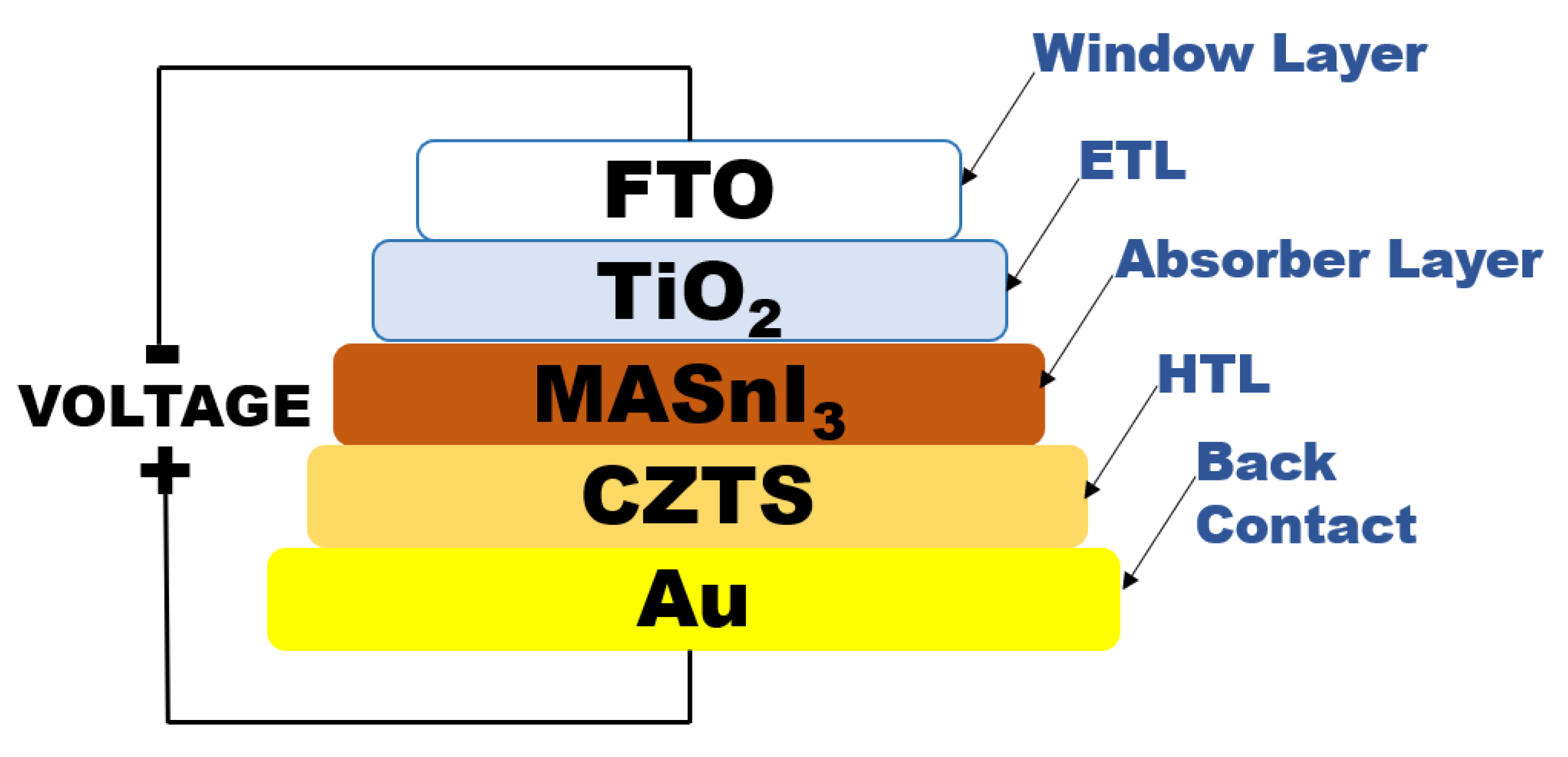
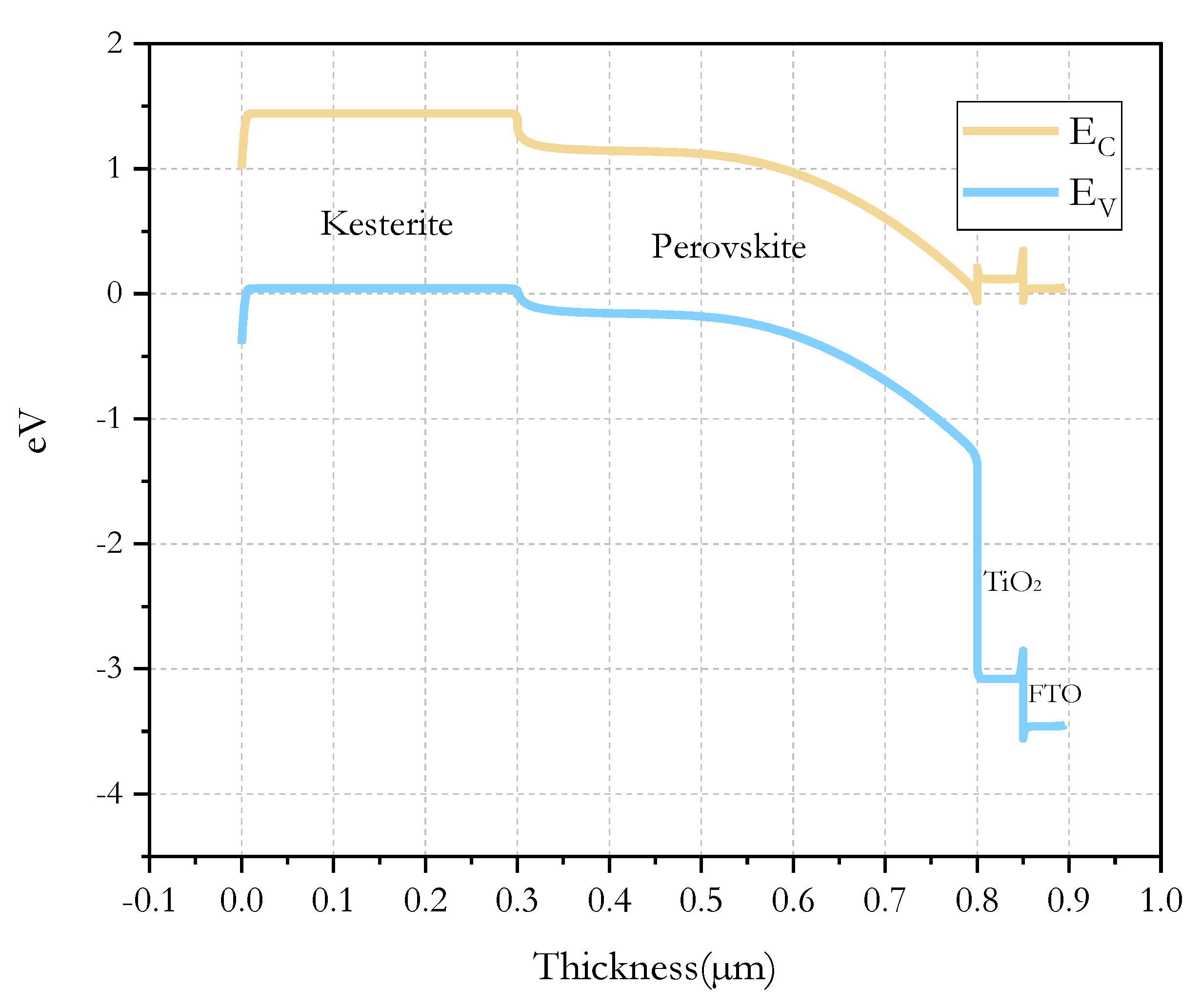
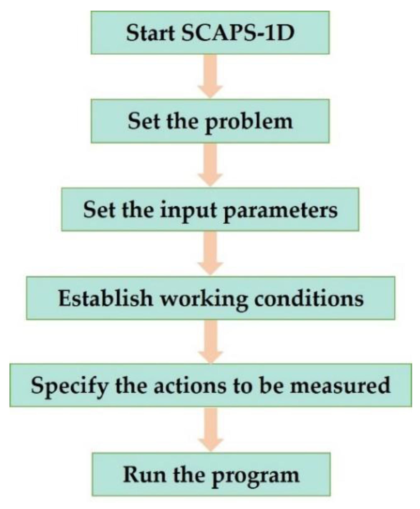
2. Materials and Methods
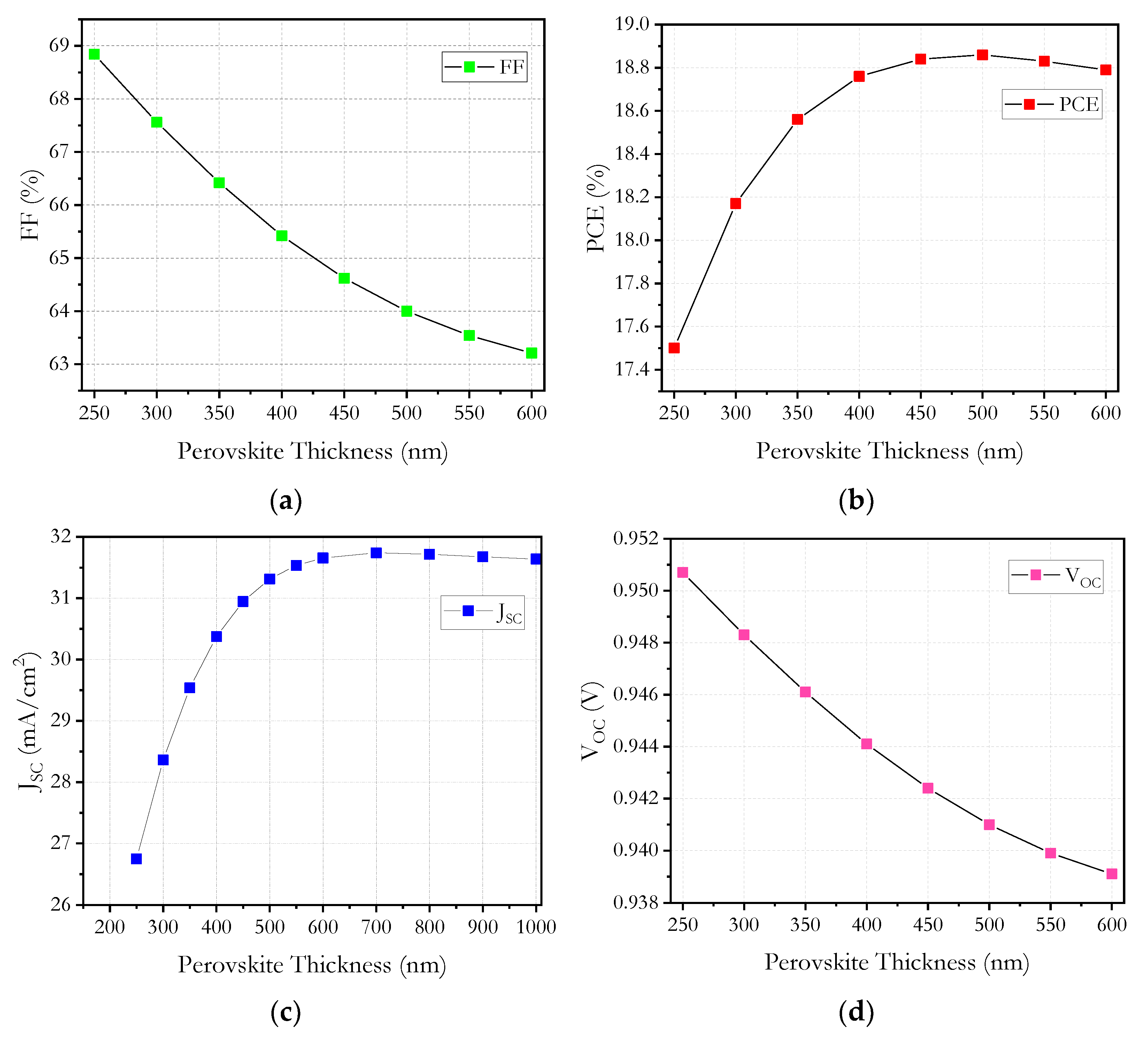
3. Analysis of Absorber Layer Thickness
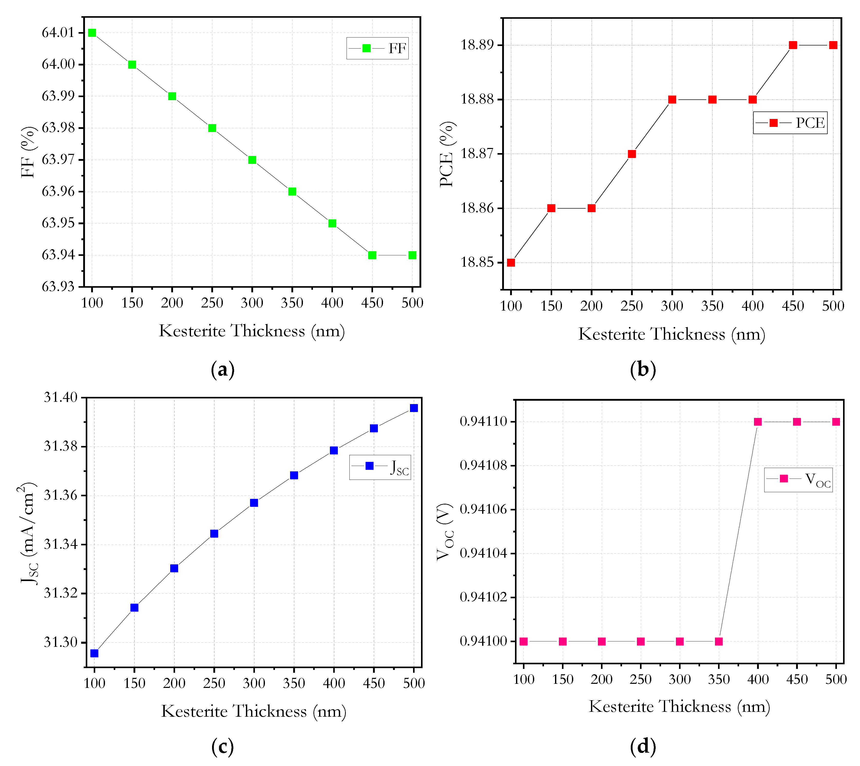
4. Analysis of Hole Transporting Layer Thickness
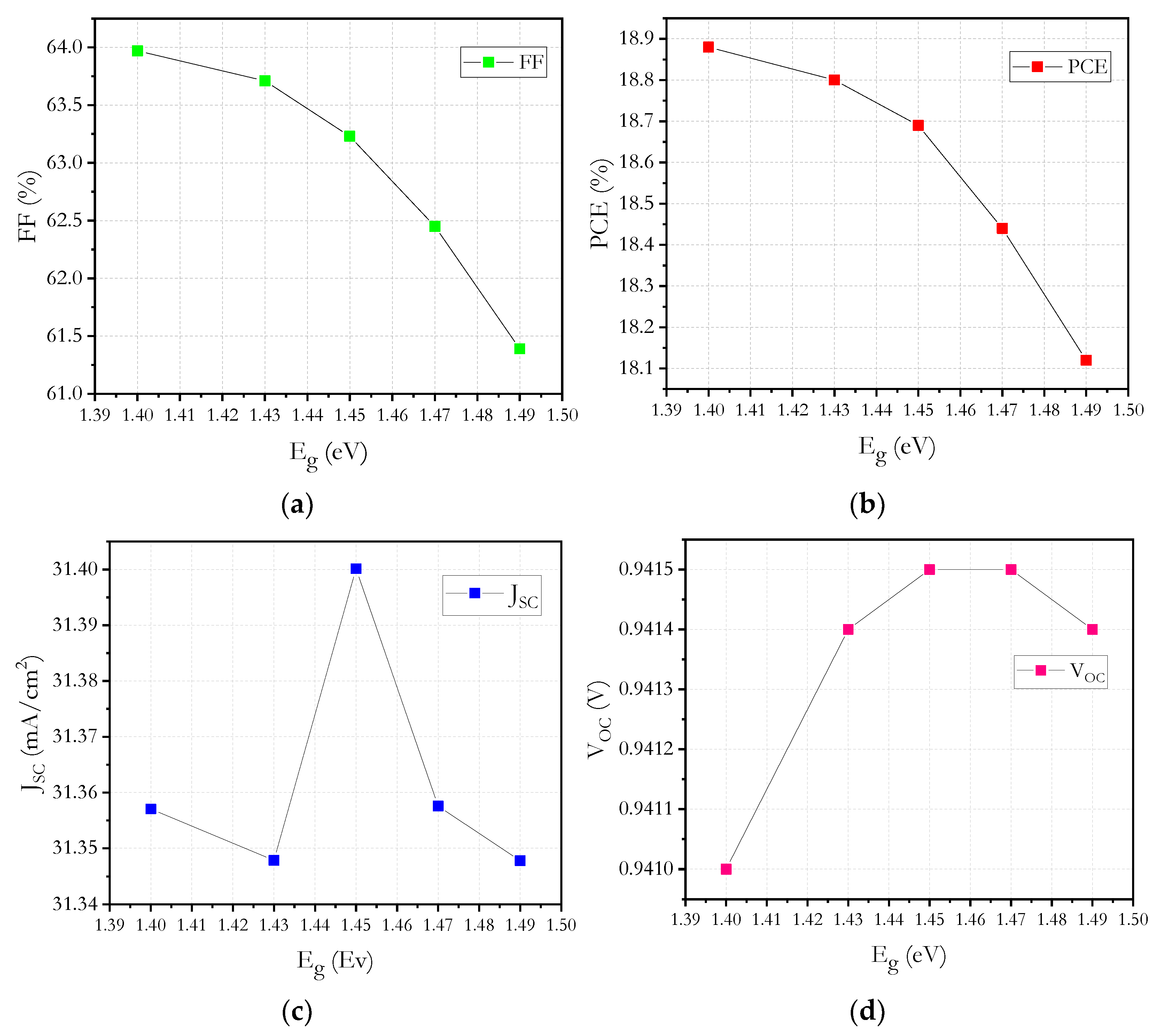
5. Tuning Band Gap Energy in Kesterite Layer (HTL)
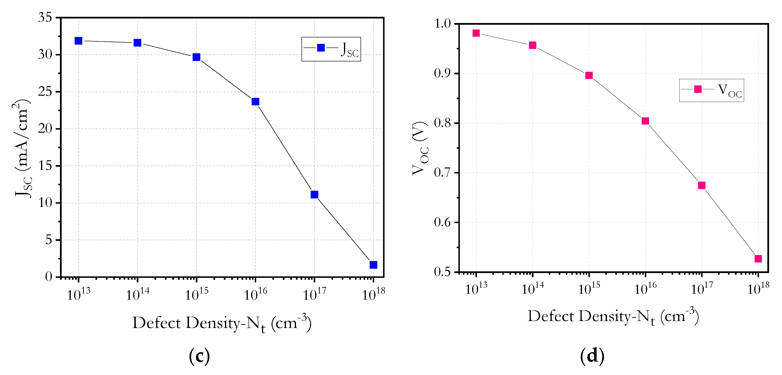
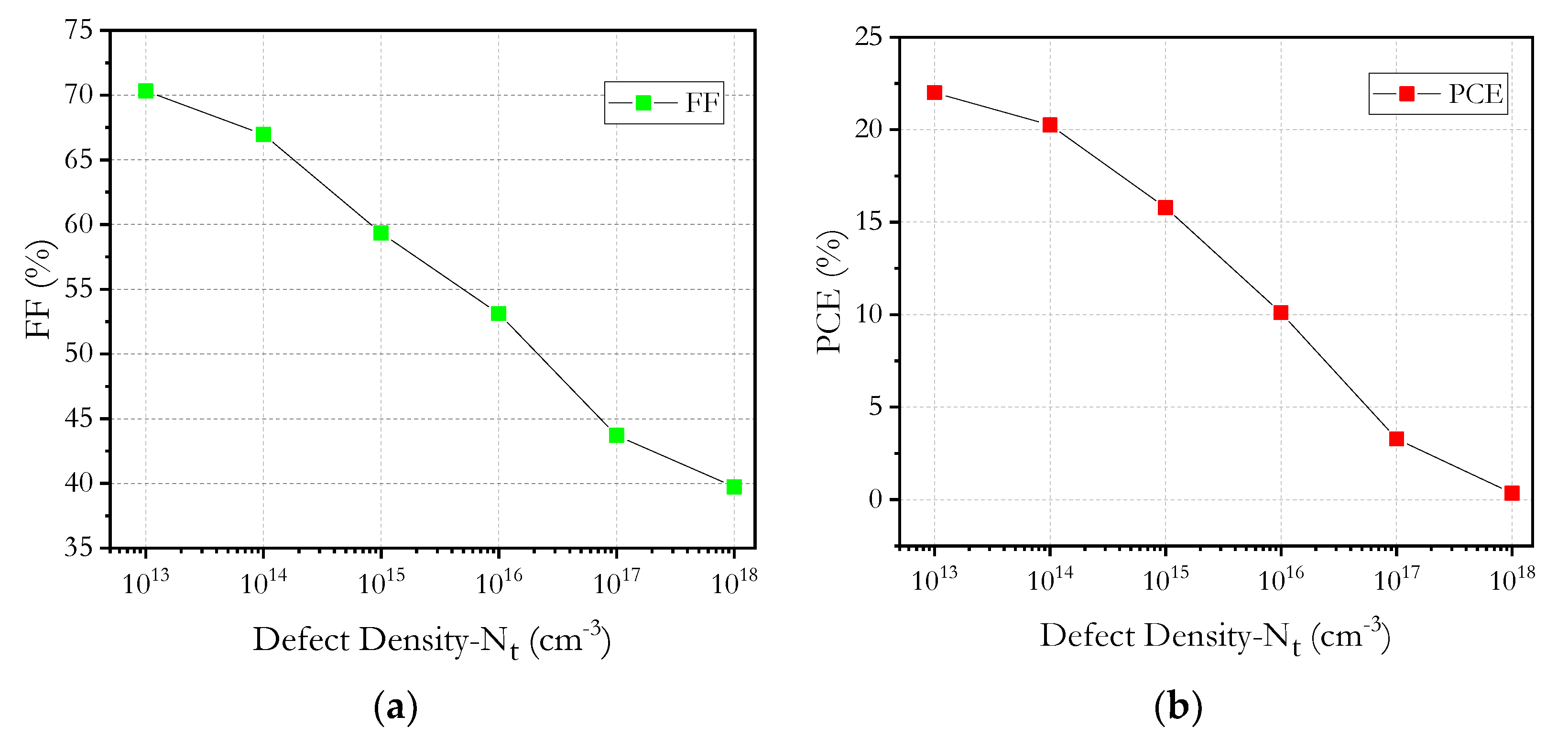
6. Analysis of Defect Density (Nt) in Absorber Layer
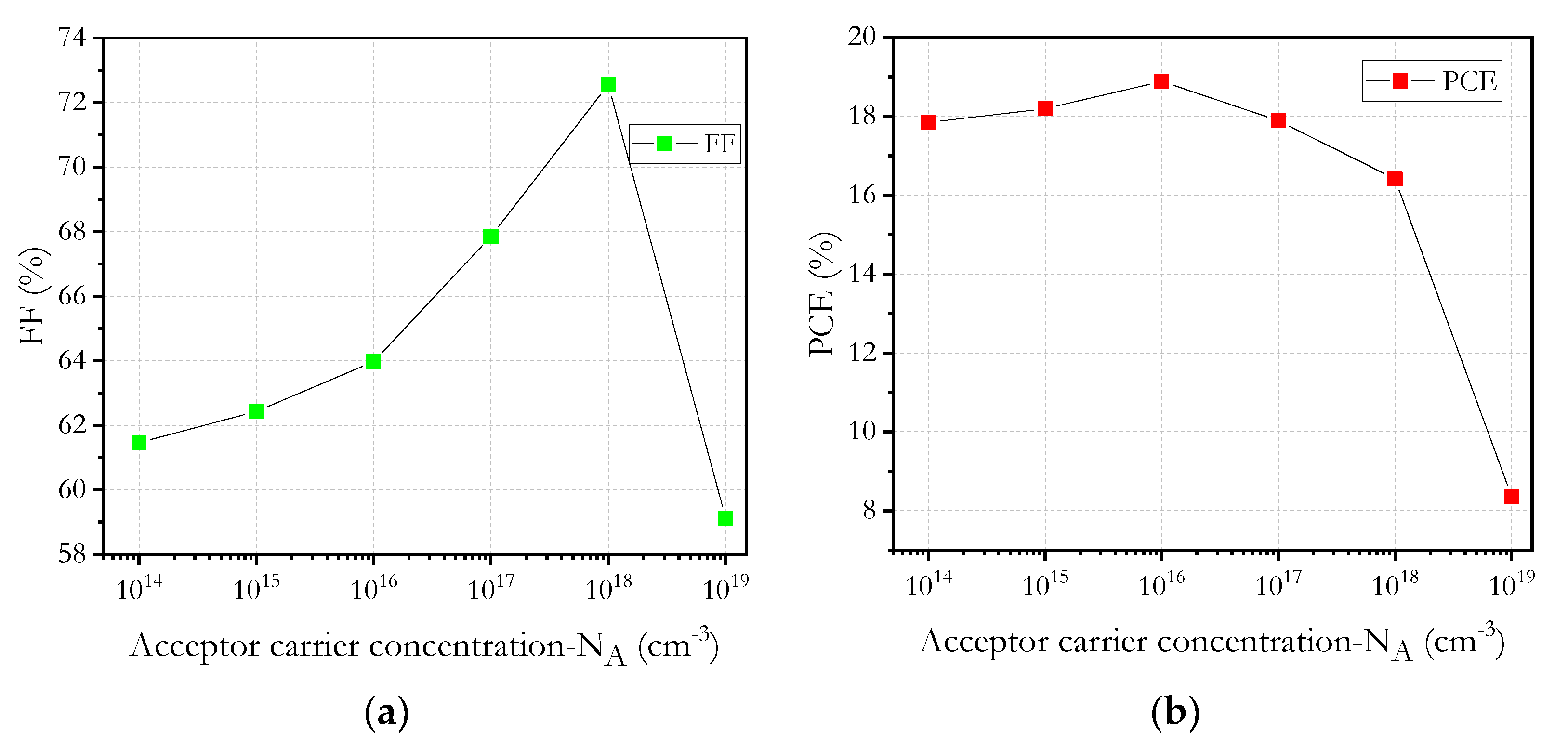
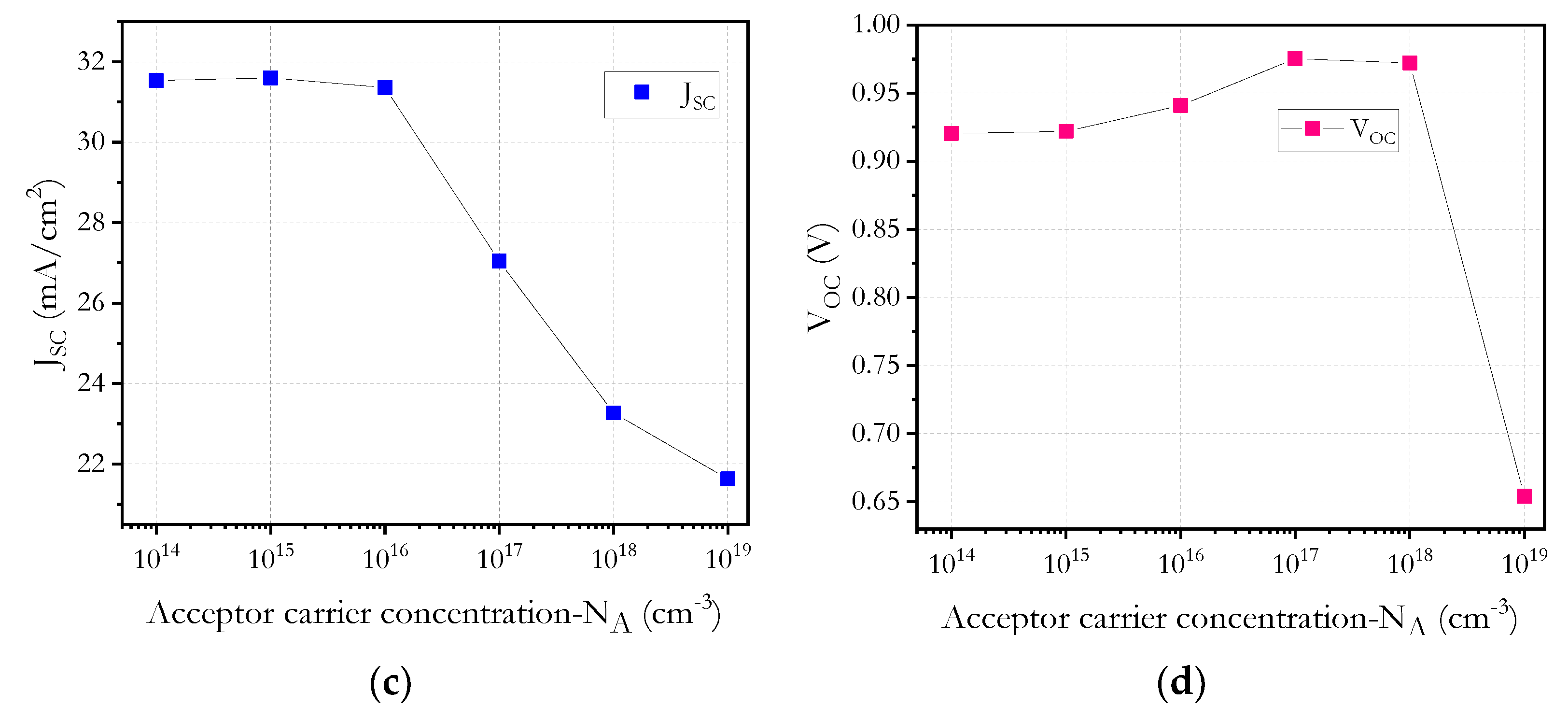
7. Analysis of Acceptor Carrier Concentration (NA) in Absorber Layer
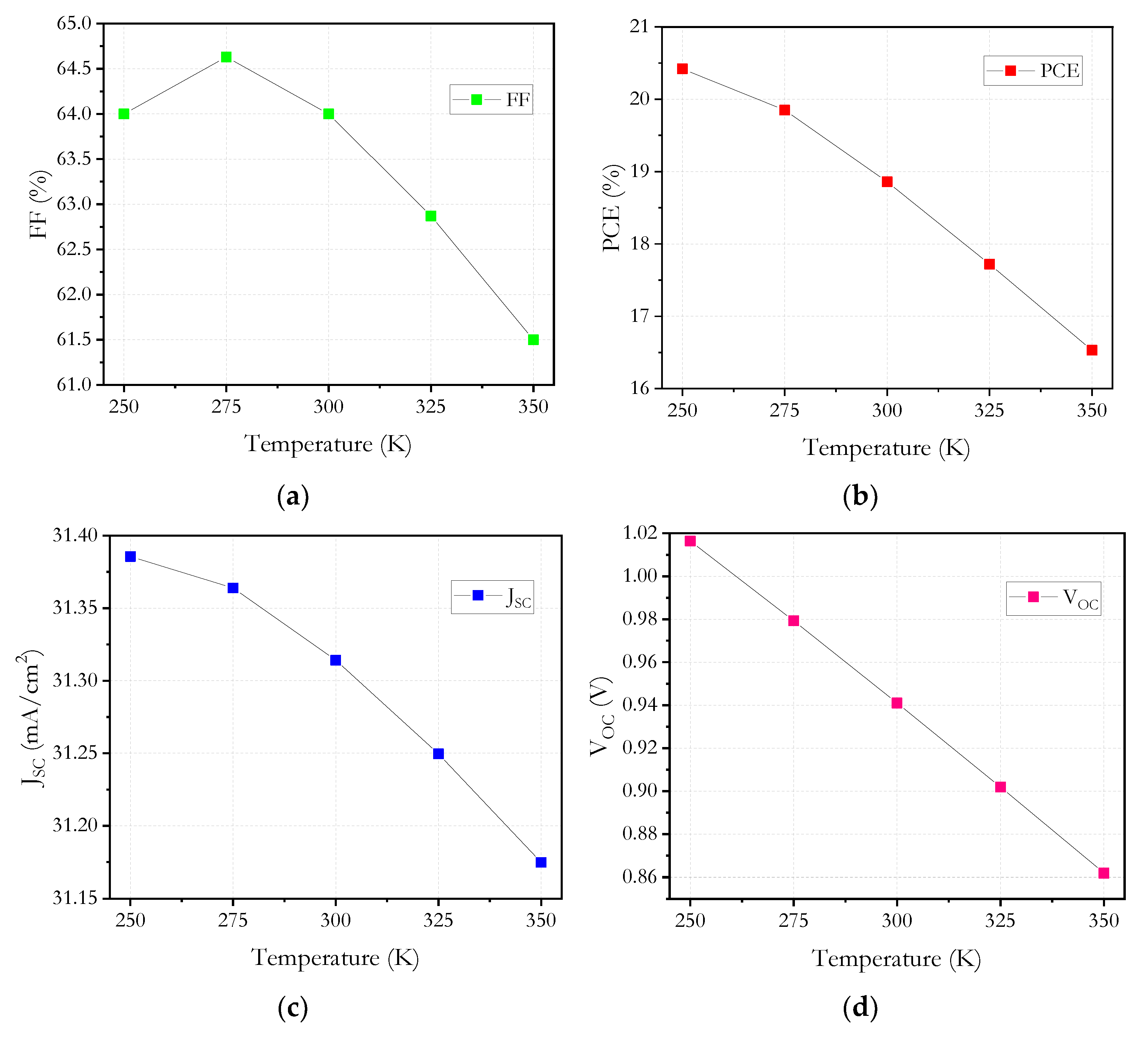
8. Effect of Operating Temperature
9. Conclusions
Author Contributions
Funding
Acknowledgments
Conflicts of Interest
References
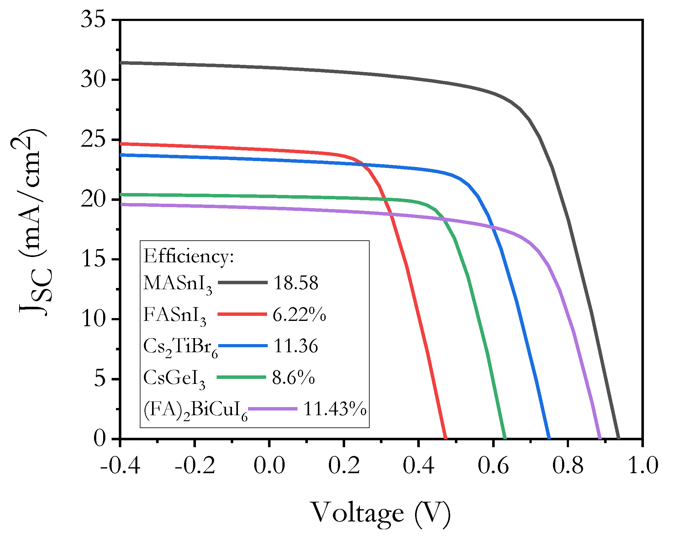
- Kiziroglou, M.E.; Yeatman, E.M. Materials and techniques for energy harvesting. Funct. Mater. Sustain. Energy Appl. 2012, 541–572. [Google Scholar]
- Jeong, Y.; Shin, D.; Park, J.H.; Park, J.; Yi, Y.; Im, S. Integrated advantages from perovskite photovoltaic cell and 2D MoTe2 transistor towards self-power energy harvesting and photosensing. Nano Energy 2019, 63, 103833. [Google Scholar] [CrossRef]
- Benami, A. Effect of CZTS Parameters on Photovoltaic Solar Cell from Numerical Simulation. J. Energy Power Eng. 2019, 13, 32–36. [Google Scholar]
- Devi, C.; Mehra, R. Device simulation of lead-free MASnI3 solar cell with CuSbS2 (copper antimony sulfide). J. Mater. Sci. 2019, 54, 5615–5624. [Google Scholar] [CrossRef]
- Fujihara, T.; Terakawa, S.; Matsushima, T.; Qin, C.; Yahiro, M.; Adachi, C. Fabrication of high coverage MASnI3 perovskite films for stable, planar heterojunction solar cells. J. Mater. Chem. C 2017, 5, 1121–1127. [Google Scholar] [CrossRef]
- Wang, Y.C.; Chang, J.; Zhu, L.; Li, X.; Song, C.; Fang, J. Electron-Transport-Layer-Assisted Crystallization of Perovskite Films for High-Efficiency Planar Heterojunction Solar Cells. Adv. Funct. Mater. 2018, 28, 1706317. [Google Scholar] [CrossRef]
- Wang, Y.C.; Huang, S.K.; Nakamura, T.; Kao, Y.T.; Chiang, C.H.; Wang, D.Y.; Chang, Y.J.; Koshida, N.; Shimada, T.; Liu, S.; et al. Quantum-assisted photoelectric gain effects in perovskite solar cells. NPG Asia Mater. 2020, 12, 54. [Google Scholar] [CrossRef]
- Baig, F.; Khattak, Y.H.; Marí, B.; Beg, S.; Gillani, S.R.; Ahmed, A. Mitigation of interface recombination by careful selection of ETL for efficiency enhancement of MASnI3 solar cell. Optik 2018, 170, 463–474. [Google Scholar] [CrossRef]
- Alam, I.; Ashraf, M.A. Effect of different device parameters on tin-based perovskite solar cell coupled with In2S3 electron transport layer and CuSCN and Spiro-OMeTAD alternative hole transport layers for high-efficiency performance. Energy Sources Part A Recovery Util. Environ. Eff. 2020, 1–17. [Google Scholar] [CrossRef]
- Patel, P.K. Device simulation of highly efficient eco-friendly CH3NH3SnI3 perovskite solar cell. Sci. Rep. 2021, 11, 3082. [Google Scholar] [CrossRef] [PubMed]
- Bhattarai, S.; Das, T.D. Optimization of the perovskite solar cell design to achieve a highly improved efficiency. Opt. Mater. 2021, 111, 110661. [Google Scholar] [CrossRef]
- Todorov, T.; Gershon, T.; Gunawan, O.; Sturdevant, C.; Guha, S. Perovskite-kesterite monolithic tandem solar cells with high open-circuit voltage. Appl. Phys. Lett. 2014, 105, 173902. [Google Scholar] [CrossRef]
- Khattak, Y.H.; Baig, F.; Toura, H.; Beg, S.; Soucase, B.M. CZTSe Kesterite as an Alternative Hole Transport Layer for MASnI3 Perovskite Solar Cells. J. Electron. Mater. 2019, 48, 5723–5733. [Google Scholar] [CrossRef]
- Wu, Q.; Xue, C.; Li, Y.; Zhou, P.; Liu, W.; Zhu, J.; Dai, S.; Zhu, C.; Yang, S. Kesterite Cu2ZnSnS4 as a Low-Cost Inorganic Hole-Transporting Material for High-Efficiency Perovskite Solar Cells. ACS Appl. Mater. Interfaces 2015, 7, 28466–28473. [Google Scholar] [CrossRef]
- Chen, S.; Walsh, A.; Luo, Y.; Yang, J.H.; Gong, X.G.; Wei, S.H. Wurtzite-derived polytypes of kesterite and stannite quaternary chalcogenide semiconductors. Phys. Rev. B Condens. Matter Mater. Phys. 2010, 82, 195203. [Google Scholar] [CrossRef] [Green Version]
- Mebarkia, C.; Dib, D.; Zerfaoui, H.; Belghit, R. Energy efficiency of a photovoltaic cell based thin films CZTS by SCAPS. J. Fundam. Appl. Sci. 2016, 8, 363. [Google Scholar] [CrossRef] [Green Version]
- Nguyen, T.H.; Kawaguchi, T.; Chantana, J.; Minemoto, T.; Harada, T.; Nakanishi, S.; Ikeda, S. Structural and Solar Cell Properties of a Ag-Containing Cu2ZnSnS4 Thin Film Derived from Spray Pyrolysis. ACS Appl. Mater. Interfaces 2018, 10, 5455–5463. [Google Scholar] [CrossRef] [PubMed]
- Elhmaidi, Z.O.; Pandiyan, R.; Abd-Lefdil, M.; Saucedo, E.; el Khakani, M.A. In-situ tuning of the zinc content of pulsed-laser-deposited CZTS films and its effect on the photoconversion efficiency of p-CZTS/n-Si heterojunction photovoltaic devices. Appl. Surf. Sci. 2020, 507, 145003. [Google Scholar] [CrossRef]
- Li, X.; Zhao, X.; Gu, Y.; Yin, X.; Nan, H.; Tai, M.; Chen, H.; Shen, H.; Lin, H. Solution-processed kesterite Cu2ZnSnS4 as efficient hole extraction layer for inverted perovskite solar cells. Chem. Lett. 2018, 47, 817–820. [Google Scholar] [CrossRef]
- Wallace, S.K.; Mitzi, D.B.; Walsh, A. The steady rise of kesterite solar cells. ACS Energy Lett. 2017, 2, 776–779. [Google Scholar] [CrossRef] [Green Version]
- Bello, I.T.; Awodele, M.K.; Adedokun, O.; Akinrinola, O.; Awodugba, A.O. Modeling and simulation of CZTS-perovskite sandwiched tandem solar cell. Turk. J. Phys. 2018, 42, 321–328. [Google Scholar]
- Slami, A.; Belkaid, A.B. Numerical Study of Based Perovskite Solar Cells by SCAPS-1D Solar cells. Int. J. Energy Environ. 2019, 13, 17–21. [Google Scholar]
- Azri, F.; Meftah, A.; Sengouga, N.; Meftah, A. Electron and hole transport layers optimization by numerical simulation of a perovskite solar cell. Sol. Energy 2019, 181, 372–378. [Google Scholar] [CrossRef]
- Abdelaziz, S.; Zekry, A.; Shaker, A.; Abouelatta, M. Investigating the performance of formamidinium tin-based perovskite solar cell by SCAPS device simulation. Opt. Mater. 2020, 101, 109738. [Google Scholar] [CrossRef]
- Chakraborty, K.; Choudhury, M.G.; Paul, S. Numerical study of Cs2TiX6 (X = Br−, I−, F− and Cl−) based perovskite solar cell using SCAPS-1D device simulation. Sol. Energy 2019, 194, 886–892. [Google Scholar] [CrossRef]
- Hussain, S.S.; Riaz, S.; Nowsherwan, G.A.; Jahangir, K.; Raza, A.; Iqbal, M.J.; Sadiq, I.; Hussain, S.M.; Naseem, S. Numerical Modeling and Optimization of Lead-Free Hybrid Double Perovskite Solar Cell by Using SCAPS-1D. J. Renew. Energy 2021, 1–12. [Google Scholar] [CrossRef]
- Raj, A.; Kumar, M.; Bherwani, H.; Gupta, A.; Anshul, A. Evidence of improved power conversion efficiency in lead-free CsGeI3 based perovskite solar cell heterostructure via scaps simulation. J. Vac. Sci. Technol. B 2021, 39, 012401. [Google Scholar] [CrossRef]
- Ashebir, G.Y.; Dong, C.; Wan, Z.; Qi, J.; Chen, J.; Zhao, Q.; Chen, W.; Wang, M. Solution-processed Cu2ZnSnS4 nanoparticle film as efficient hole transporting layer for stable perovskite solar cells. J. Phys. Chem. Solids 2019, 129, 204–208. [Google Scholar] [CrossRef]
- Ghahremanirad, E.; Olyaee, S.; Nejand, B.A.; Nazari, P.; Ahmadi, V.; Abedi, K. Improving the performance of perovskite solar cells using kesterite mesostructure and plasmonic network. Sol. Energy 2018, 169, 498–504. [Google Scholar] [CrossRef]
- Yuan, M.; Zhang, X.; Kong, J.; Zhou, W.; Zhou, Z.; Tian, Q.; Meng, Y.; Wu, S.; Kou, D. Controlling the Band Gap to Improve Open-Circuit Voltage in Metal Chalcogenide based Perovskite Solar Cells. Electrochim. Acta 2016, 215, 374–379. [Google Scholar] [CrossRef]
- Khanzada, L.S.; Levchuk, I.; Hou, Y.; Azimi, H.; Osvet, A.; Ahmad, R.; Brandl, M.; Herre, P.; Distaso, M.; Hock, R.; et al. Effective Ligand Engineering of the Cu2ZnSnS4 Nanocrystal Surface for Increasing Hole Transport Efficiency in Perovskite Solar Cells. Adv. Funct. Mater. 2016, 26, 8300–8306. [Google Scholar] [CrossRef]
- Patel, S.B.; Patel, A.H.; Gohel, J.V. A novel and cost effective CZTS hole transport material applied in perovskite solar cells. CrystEngComm 2018, 20, 7677–7687. [Google Scholar] [CrossRef]
- Simya, O.K.; Mahaboobbatcha, A.; Balachander, K. A comparative study on the performance of Kesterite based thin film solar cells using SCAPS simulation program. Superlattices Microstruct. 2015, 82, 248–261. [Google Scholar] [CrossRef]
- Ojeda-Durán, E.; Monfil-Leyva, K.; Andrade-Arvizu, J.; Becerril-Romero, I.; Sánchez, Y.; Fonoll-Rubio, R.; Guc, M.; Jehl, Z.; Luna-López, J.A.; Muñoz-Zurita, A.L.; et al. CZTS solar cells and the possibility of increasing VOC using evaporated Al2O3 at the CZTS/CdS interface. Sol. Energy 2020, 198, 696–703. [Google Scholar] [CrossRef]
- Sahu, M.; Reddy, V.R.M.; Park, C.; Sharma, P. Review article on the lattice defect and interface loss mechanisms in kesterite materials and their impact on solar cell performance. Sol. Energy 2021, 230, 13–58. [Google Scholar] [CrossRef]
- Khattak, Y.H.; Baig, F.; Toura, H.; Ullah, S.; Marí, B.; Beg, S.; Ullah, H. Effect of CZTSe BSF and minority carrier life time on the efficiency enhancement of CZTS kesterite solar cell. Curr. Appl. Phys. 2018, 18, 633–641. [Google Scholar] [CrossRef]
- Wu, N.; Wu, Y.; Walter, D.; Shen, H.; Duong, T.; Grant, D.; Barugkin, C.; Fu, X.; Peng, J.; White, T.; et al. Identifying the Cause of Voltage and Fill Factor Losses in Perovskite Solar Cells by Using Luminescence Measurements. Energy Technol. 2017, 5, 1827–1835. [Google Scholar] [CrossRef] [Green Version]
- Liu, F.; Zhu, J.; Wei, J.; Li, Y.; Lv, M.; Yang, S.; Zhang, B.; Yao, J.; Dai, S. Numerical simulation: Toward the design of high-efficiency planar perovskite solar cells. Appl. Phys. Lett. 2014, 104, 253508. [Google Scholar] [CrossRef]
- Liu, Q.; Fan, L.; Zhang, Q.E.; Zhou, A.A.; Wang, B.; Bai, H.; Tian, Q.; Fan, B.; Zhang, T. Benzoyl Peroxide as an Efficient Dopant for Spiro-OMeTAD in Perovskite Solar Cells. ChemSusChem 2017, 10, 3098–3104. [Google Scholar] [CrossRef]
- Li, M.; Wang, J.; Jiang, A.; Xia, D.; Du, X.; Dong, Y.; Wang, P.; Fan, R.; Yang, Y. Metal organic framework doped Spiro-OMeTAD with increased conductivity for improving perovskite solar cell performance. Sol. Energy 2019, 188, 380–385. [Google Scholar] [CrossRef]
- Tan, K.; Lin, P.; Wang, G.; Liu, Y.; Xu, Z.; Lin, Y. Controllable design of solid-state perovskite solar cells by SCAPS device simulation. Solid-State Electron. 2016, 126, 75–80. [Google Scholar] [CrossRef]
- Adewoyin, A.D.; Olopade, M.A.; Oyebola, O.O.; Chendo, M.A. Development of CZTGS/CZTS tandem thin film solar cell using SCAPS-1D. Optik 2019, 176, 132–142. [Google Scholar] [CrossRef]
- Baig, F.; Khattak, Y.H.; Marí, B.; Beg, S.; Ahmed, A.; Khan, K. Efficiency Enhancement of CH3NH3SnI3 Solar Cells by Device Modeling. J. Electron. Mater. 2018, 47, 5275–5282. [Google Scholar] [CrossRef]
- Roy, P.; Sinha, N.K.; Khare, A. An investigation on the impact of temperature variation over the performance of tin-based perovskite solar cell: A numerical simulation approach. Mater. Today Proc. 2019, 39, 2022–2026. [Google Scholar] [CrossRef]


| Solar Cell Structure | Voc (V) | Jsc (mA/cm2) | FF (%) | PCE (%) | Ref. |
|---|---|---|---|---|---|
| o/Cu2ZnSn(S,Se)4/CdS/ITO/PEDOT:PSS/CH3NH3PbI3/PCBM/Al | 1.40 | 15.50 | 73.60 | 16.00 | [12] |
| FTO/TiO2/MASnI3/CZTSe | 0.86 | 29.45 | 76.74 | 19.52 | [13] |
| FTO/TiO2/CH3NH3SnI3/CZTS/Au | 1.06 | 20.54 | 58.70 | 12.75 | [14] |
| FTO/TiO2/CH3NH3SnI3/CZTS/Au | 0.94 | 20.31 | 72.00 | 13.75 | [19] |
| ITO/CZST/CH3NH3PbI3/PCBM/BCP/Ag | 0.82 | 9.70 | 76.10 | 6.02 | [28] |
| ITO/NiO/meso-CZTSe: MAPbI3/ZnO/Al | 1.05 | 19.19 | 83.30 | 16.80 | [29] |
| FTO/TiO2/CH3NH3PbI3/CZTS/Ag | 0.94 | 18.75 | 60.50 | 10.72 | [30] |
| ITO/LT-CZTS/Perovskite/PCBM/PrCMA/Ag | 0.92 | 20.70 | 81.00 | 15.40 | [31] |
| FTO/TiO2/ZnO/CH3NH3Pb0.5Sn0.5I3−yCly/CZTS/Pt-FTO | 0.79 | 19.10 | 64.00 | 9.66 | [32] |
| FTO/TiO2/MASnI3/CZTS/Au (this work [T.W.]) | 0.96 | 31.66 | 67.00 | 20.28 | [T.W.] |
| Parameters | Symbol | p-CZTS | i-MASnI3 | n-TiO2 | n-FTO |
|---|---|---|---|---|---|
| Thickness | W (nm) | 300 | 500 | 50 | 50 |
| Band gap | Eg (eV) | 1.4 | 1.3 | 3.2 | 3.5 |
| Electron affinity | X (eV) | 4.1 | 4.17 | 3.9 | 4.3 |
| Dielec. Permittivity | Ԑr | 9 | 8.2 | 9 | 9 |
| (Conduction Band) Effective density of states | NC (cm−3) | 2.20 × 10¹⁸ | 2.80 × 10¹⁸ | 1.00 × 10²¹ | 1.00 × 10¹⁹ |
| (Valence Band) Effective | NV (cm−3) | 1.80 × 10¹⁸ | 3.90 × 10¹⁸ | 2.00 × 10²⁰ | 1.00 × 10¹⁹ |
| Electron mobility | µe (cm2/Vs) | 1.00 × 10² | 1.60 × 10⁻¹ | 2.50 × 10 | 2.50 × 10 |
| Hole mobility | µp (cm2/Vs | 1.25 × 10 | 1.60 × 10⁻¹ | 1.00 × 10² | 1.00 × 10² |
| Shallow uniform donor | n (1/cm3) | / | / | 1.00 × 10¹⁹ | 2.00 × 10¹⁸ |
| Shallow uniform acceptor | p (1/cm3) | 1.00 × 10¹⁹ | 1.00 × 10¹⁶ | / | / |
| Parameters | Symbol | Au | FTO |
|---|---|---|---|
| Metal work function | ϕ (eV) | 5.1 | 4.4 |
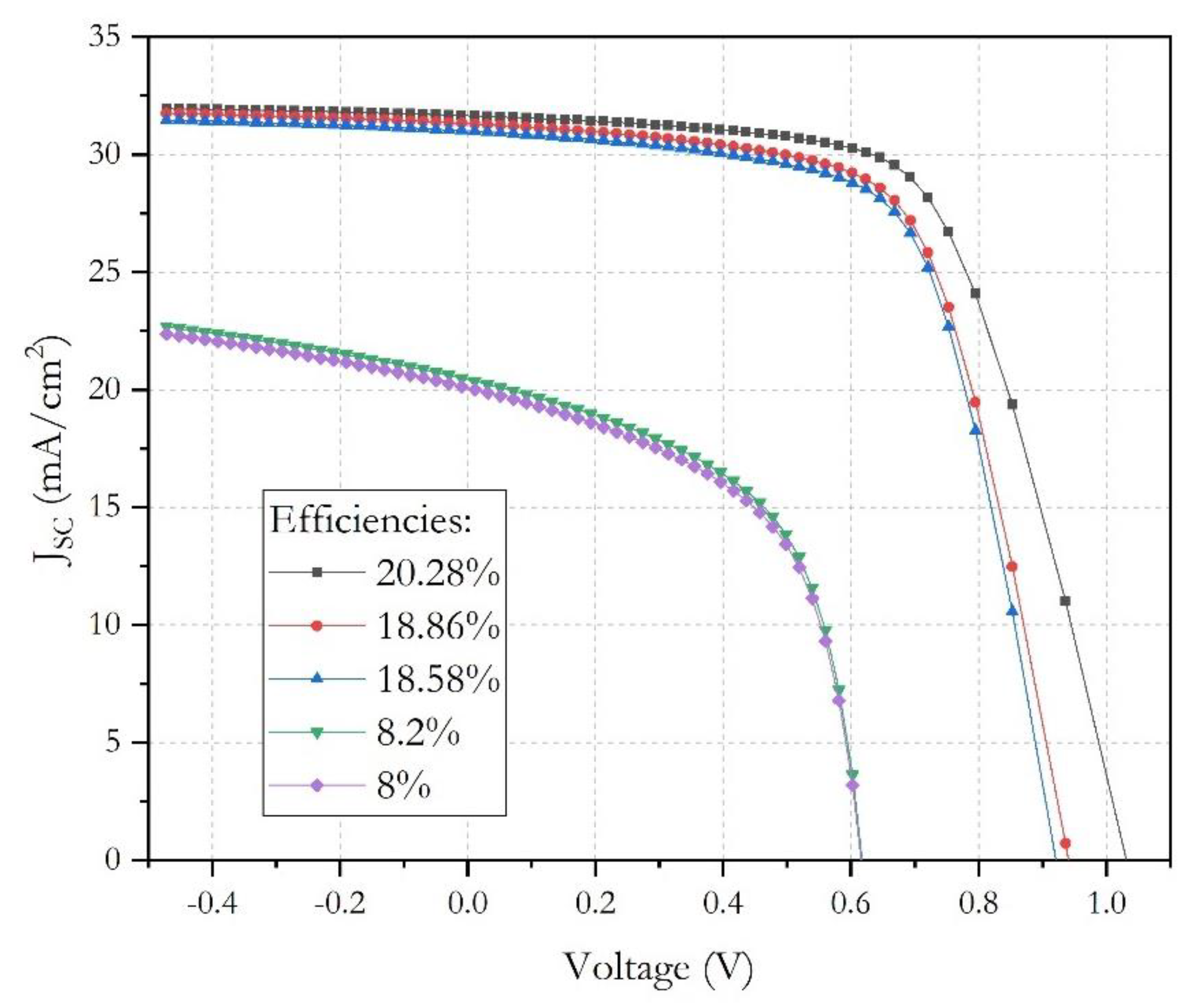
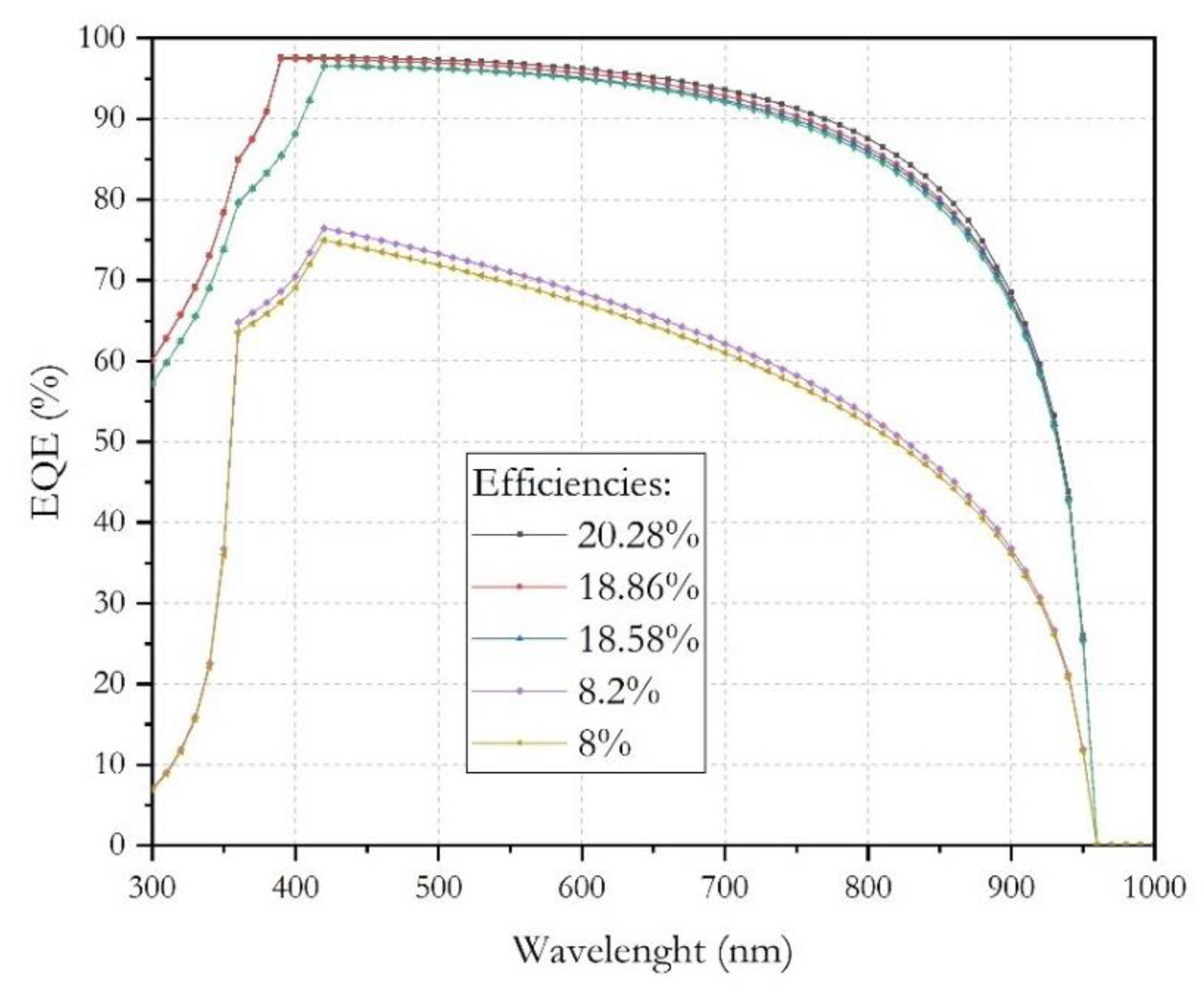
| Voc (V) | Jsc (mA/cm2) | FF (%) | PCE (%) | Perovskite NA | Perovskite Nt | Kesterite (nm) | TiO2 (eV) | TiO2 ND |
|---|---|---|---|---|---|---|---|---|
| 0.77 | 20.45 | 51 | 8.00 | 1.00 × 10¹⁶ | 2.00 × 10¹⁵ | 100 | 3 | 9.00 × 10¹⁶ |
| 0.77 | 20.78 | 51 | 8.20 | 1.00 × 10¹⁶ | 2.00 × 10¹⁵ | 100 | 3 | 1.00 × 10¹⁸ |
| 0.94 | 31.00 | 64 | 18.58 | 1.00 × 10¹⁶ | 2.00 × 10¹⁴ | 100 | 3 | 1.00 × 10¹⁹ |
| 0.94 | 31.31 | 64 | 18.86 | 1.00 × 10¹⁹ | 1.00 × 10¹⁴ | 150 | 3.2 | 1.00 × 10¹⁹ |
| 0.96 | 31.66 | 67 | 20.28 | 1.00 × 10¹⁹ | 1.00 × 10¹⁴ | 300 | 3.2 | 1.00 × 10¹⁹ |
Publisher’s Note: MDPI stays neutral with regard to jurisdictional claims in published maps and institutional affiliations. |
© 2021 by the authors. Licensee MDPI, Basel, Switzerland. This article is an open access article distributed under the terms and conditions of the Creative Commons Attribution (CC BY) license (https://creativecommons.org/licenses/by/4.0/).
Share and Cite
Piñón Reyes, A.C.; Ambrosio Lázaro, R.C.; Monfil Leyva, K.; Luna López, J.A.; Flores Méndez, J.; Heredia Jiménez, A.H.; Muñoz Zurita, A.L.; Severiano Carrillo, F.; Ojeda Durán, E. Study of a Lead-Free Perovskite Solar Cell Using CZTS as HTL to Achieve a 20% PCE by SCAPS-1D Simulation. Micromachines 2021, 12, 1508. https://doi.org/10.3390/mi12121508
Piñón Reyes AC, Ambrosio Lázaro RC, Monfil Leyva K, Luna López JA, Flores Méndez J, Heredia Jiménez AH, Muñoz Zurita AL, Severiano Carrillo F, Ojeda Durán E. Study of a Lead-Free Perovskite Solar Cell Using CZTS as HTL to Achieve a 20% PCE by SCAPS-1D Simulation. Micromachines. 2021; 12(12):1508. https://doi.org/10.3390/mi12121508
Chicago/Turabian StylePiñón Reyes, Ana C., Roberto C. Ambrosio Lázaro, Karim Monfil Leyva, José A. Luna López, Javier Flores Méndez, Aurelio H. Heredia Jiménez, Ana L. Muñoz Zurita, Francisco Severiano Carrillo, and Esteban Ojeda Durán. 2021. "Study of a Lead-Free Perovskite Solar Cell Using CZTS as HTL to Achieve a 20% PCE by SCAPS-1D Simulation" Micromachines 12, no. 12: 1508. https://doi.org/10.3390/mi12121508
APA StylePiñón Reyes, A. C., Ambrosio Lázaro, R. C., Monfil Leyva, K., Luna López, J. A., Flores Méndez, J., Heredia Jiménez, A. H., Muñoz Zurita, A. L., Severiano Carrillo, F., & Ojeda Durán, E. (2021). Study of a Lead-Free Perovskite Solar Cell Using CZTS as HTL to Achieve a 20% PCE by SCAPS-1D Simulation. Micromachines, 12(12), 1508. https://doi.org/10.3390/mi12121508