In-Built N+ Pocket Electrically Doped Tunnel FET With Improved DC and Analog/RF Performance


Abstract
:1. Introduction
2. Device Structure and Operating Principle
3. Simulation Results and Discussions
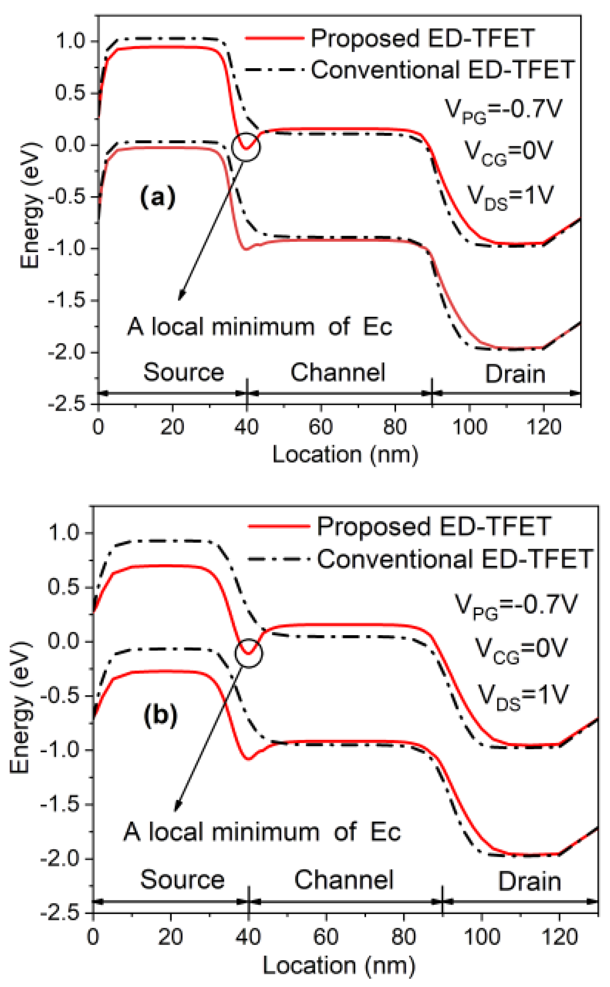
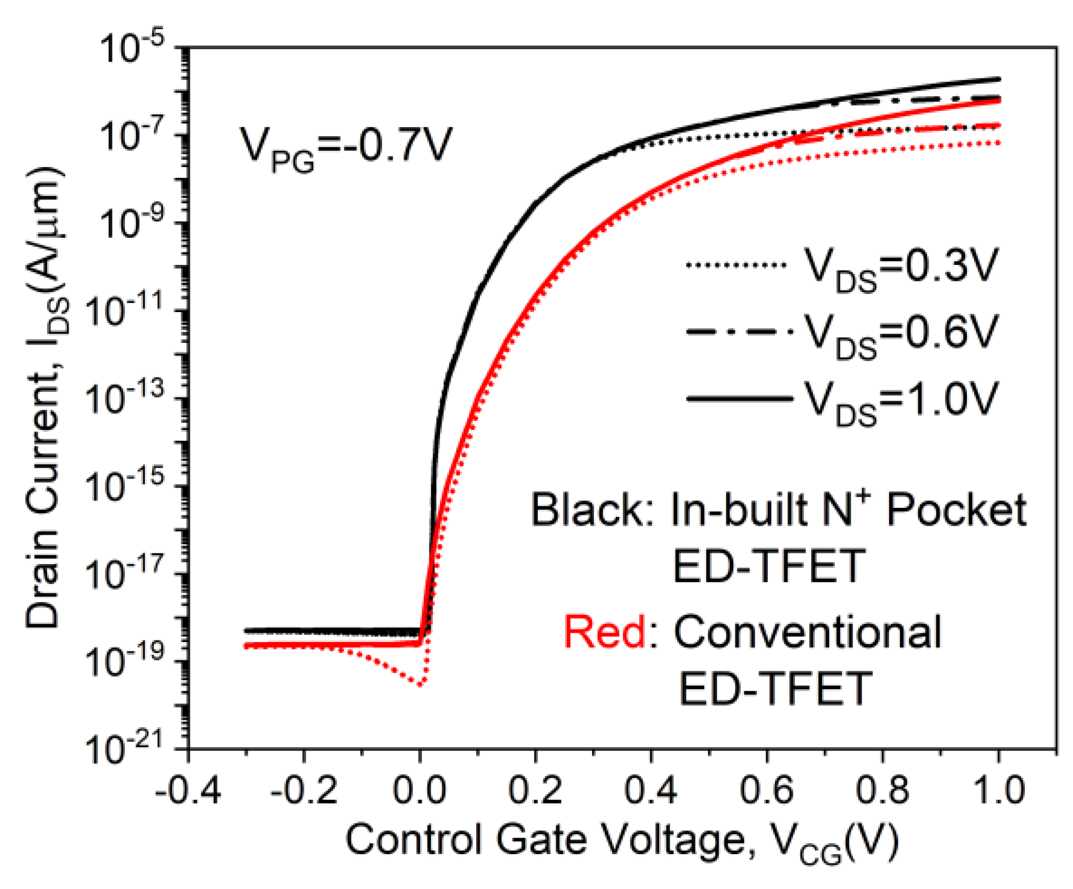
3.1. DC Characteristics
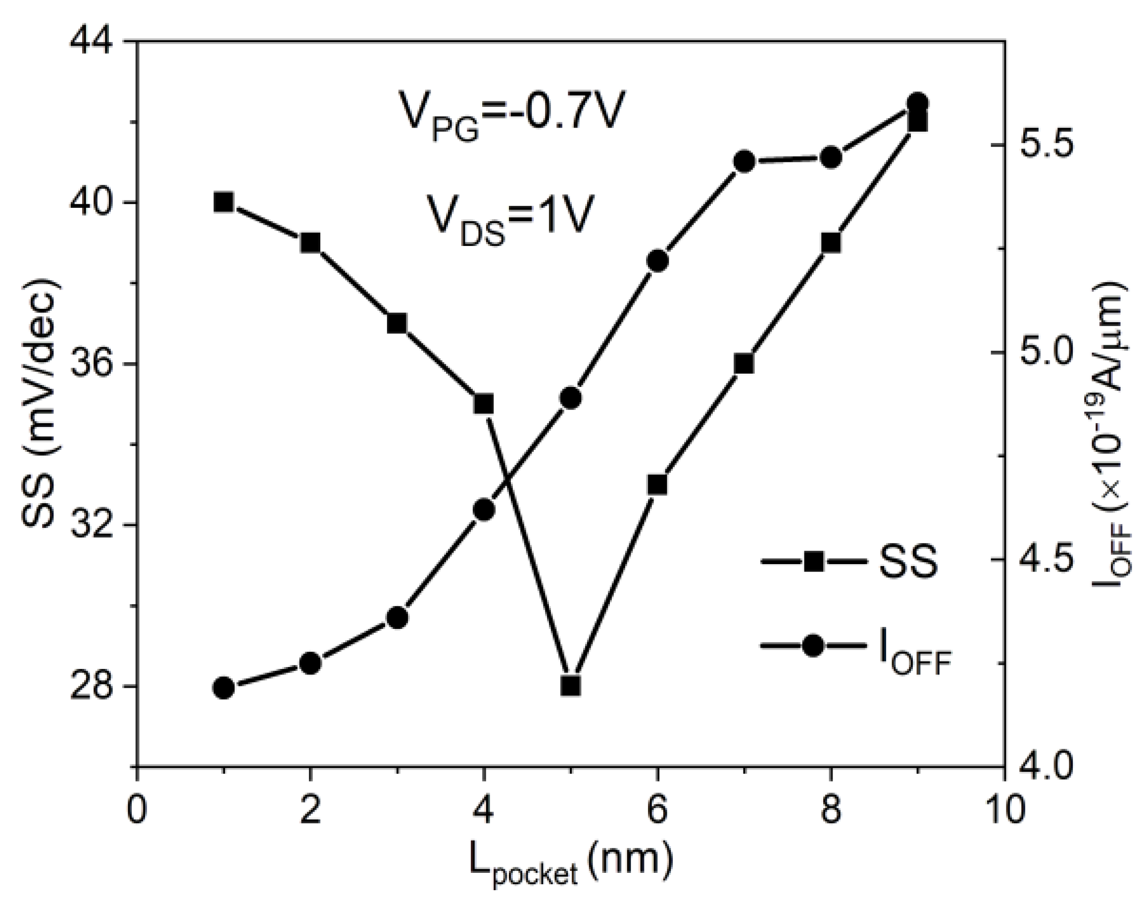
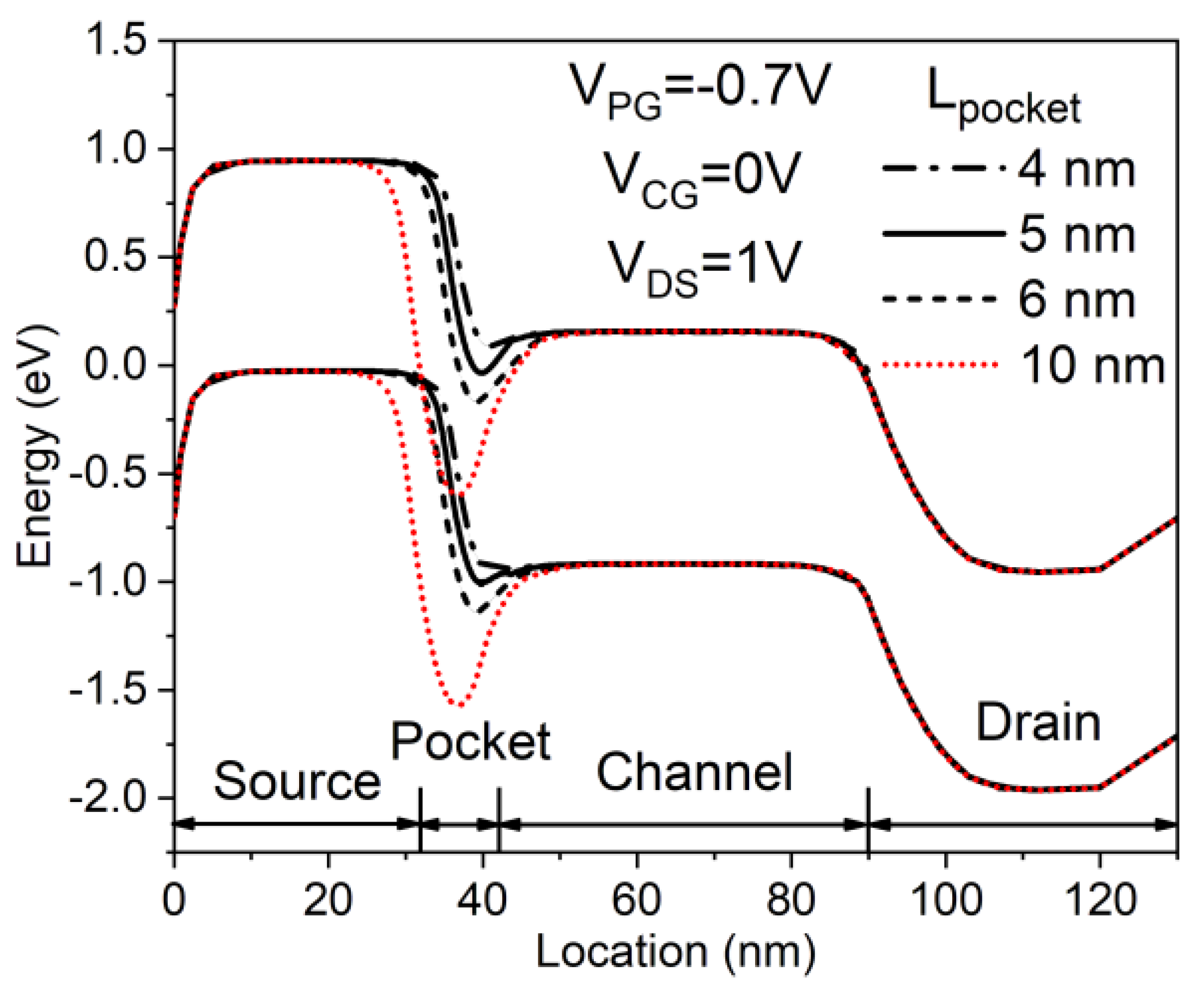
3.2. Device Optimizations
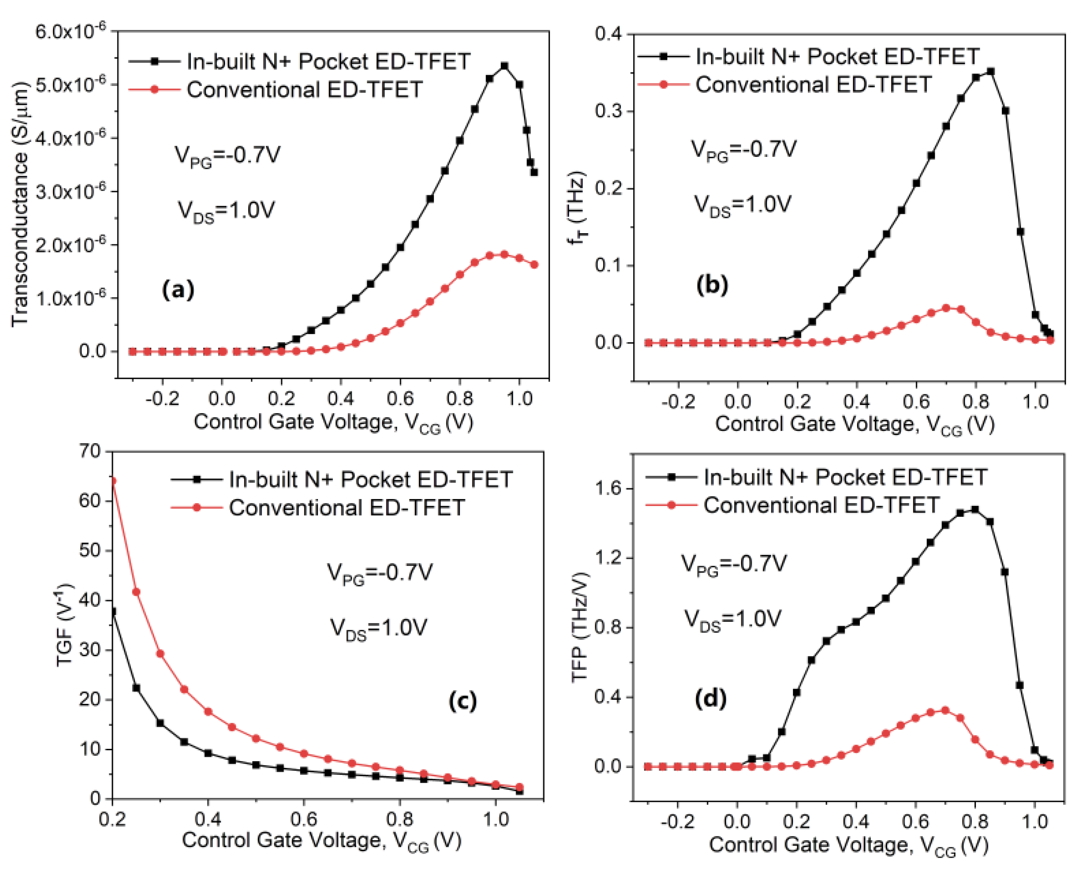
3.3. Analog/RF Performance
4. Conclusions
Author Contributions
Funding
Conflicts of Interest
References
- Tamersit, K. Computational study of p-n carbon nanotube tunnel field-effect transistor. IEEE Trans. Electron Devices 2020, 67, 704–710. [Google Scholar] [CrossRef]
- Saurabh, S.; Kumar, M.J. Novel attributes of a dual material gate nanoscale tunnel field-effect transistor. IEEE Trans. Electron Devices 2010, 58, 404–410. [Google Scholar] [CrossRef] [Green Version]
- Bhattacharyya, A.; De Chanda, M.D. Performance assessment of new dual-pocket vertical heterostructure tunnel FET-based biosensor considering steric hindrance issue. IEEE Trans. Electron Devices 2019, 66, 3988–3993. [Google Scholar] [CrossRef]
- Ghosh, B.; Akram, M.W. Junctionless tunnel field effect transistor. IEEE Electron Device Lett. 2013, 34, 584–586. [Google Scholar] [CrossRef]
- Shaikh, M.R.U.; Loan, S.A. Drain-engineered TFET with fully suppressed ambipolarity for high-frequency application. IEEE Trans. Electron Devices 2019, 66, 1628–1634. [Google Scholar] [CrossRef]
- Tura, A.; Woo, J.C.S. Performance comparison of silicon steep subthreshold FETs. IEEE Trans. Electron Devices 2010, 57, 1362–1368. [Google Scholar] [CrossRef]
- Nagavarapu, V.; Jhaveri, R.; Woo, J.C.S. The tunnel source (PNPN) n-MOSFET: A novel high performance transistor. IEEE Trans. Electron Devices 2008, 55, 1013–1019. [Google Scholar] [CrossRef]
- Cho, S.; Kang, I.M. Design optimization of tunneling field-effect transistor based on silicon nanowire PNPN structure and its radio frequency characteristics. Curr. Appl. Phys. 2012, 12, 673–677. [Google Scholar] [CrossRef]
- Cao, W.; Yao, C.J.; Jiao, G.F.; Huang, D.; Yu, H.Y.; Li, M.F. Improvement in reliability of tunneling field-effect transistor with pnin structure. IEEE Trans. Electron Devices 2011, 58. [Google Scholar] [CrossRef]
- Verreck, D.; Verhulst, A.S.; Kao, K.H.; Vandenberghe, W.G.; De Meyer, K.; Groeseneken, G. Quantum mechanical performance predictions of pnin versus pocketed line tunnel field-effect transistors. IEEE Trans. Electron Device 2013, 60, 2128–2134. [Google Scholar] [CrossRef]
- Jhaveri, R.; Nagavarapu, V.; Woo, J.C.S. Effect of pocket doping and annealing schemes on the source-pocket tunnel field-effect transistor. IEEE Trans. Electron Devices 2010, 58, 80–86. [Google Scholar] [CrossRef]
- Tura, A.; Zhang, Z.; Liu, P.; Xie, Y.H.; Woo, J.C. Vertical silicon pnpn tunnel nMOSFET with MBE-grown tunneling junction. IEEE Trans. Electron Devices 2011, 58, 1907–1913. [Google Scholar] [CrossRef]
- Chang, H.Y.; Adams, B.; Chien, P.Y.; Li, J.; Woo, J.C. Improved subthreshold and output characteristics of source-pocket Si tunnel FET by the application of laser annealing. IEEE Trans. Electron Devices 2012, 60, 92–96. [Google Scholar] [CrossRef]
- Zhang, Y.; Chu, H. Tunneling Field Effect Transistor (TFET) with Ultra-Shallow Pockets Formed by Asymmetric Ion Implantation and Method of Making Same. US Patent 20140158990, 12 June 2014. [Google Scholar]
- De Marchi, M.; Zhang, J.; Frache, S.; Sacchetto, D.; Gaillardon, P.E.; Leblebici, Y.; De Micheli, G. Configurable logic gates using polarity-controlled silicon nanowire gate-all-around FETs. IEEE Electron Device Lett. 2014, 35, 880–882. [Google Scholar] [CrossRef] [Green Version]
- De Marchi, M.; Sacchetto, D.; Frache, S.; Zhang, J.; Gaillardon, P.E.; Leblebici, Y.; De Micheli, G. Polarity control in double-gate, gate-all-around vertically stacked silicon nanowire FETs. In Proceedings of the 2012 International Electron Devices Meeting, San Francisco, CA, USA, 10–13 December 2012. [Google Scholar] [CrossRef] [Green Version]
- Lahgere, A.; Sahu, C.; Singh, J. PVT-aware design of dopingless dynamically configurable tunnel FET. IEEE Trans. Electron Devices 2015, 62, 2404–2409. [Google Scholar] [CrossRef]
- Zervas, M.; Sacchetto, D.; De Micheli, G.; Leblebici, Y. Top-down fabrication of very-high density vertically stacked silicon nanowire arrays with low temperature budget. Microelectron. Eng. 2011, 88, 3127–3132. [Google Scholar] [CrossRef] [Green Version]
- Kondekar, P.N.; Nigam, K.; Pandey, S.; Sharma, D. Design and analysis of polarity controlled electrically doped tunnel FET with bandgap engineering for analog/RF applications. IEEE Trans. Electron Devices 2016, 64, 412–418. [Google Scholar] [CrossRef]
- Choi, W.Y.; Lee, W. Hetero-gate-dielectric tunneling field-effect transistors. IEEE Trans. Electron Devices 2010, 57, 2317–2319. [Google Scholar] [CrossRef]
- Abdi, D.B.; Kumar, M.J. In-built N+ pocket pnpn tunnel field-effect transistor. IEEE Electron Device Lett. 2014, 35, 1170–1172. [Google Scholar] [CrossRef]
- Ram, M.S.; Abdi, D.B. Dopingless PNPN tunnel FET with improved performance: Design and analysis. Superlattices Microstruct. 2015, 82, 430–437. [Google Scholar] [CrossRef]
- ATLAS Device Simulation Software; Silvaco: Santa Clara, CA, USA, 2018.
- Padilla, J.L.; Gamiz, F.; Godoy, A. Impact of quantum confinement on gate threshold voltage and subthreshold swings in double-gate tunnel FETs. IEEE Trans. Electron Devices 2012, 59, 3205–3211. [Google Scholar] [CrossRef]
- Fahad, H.M.; Hussain, M.M. High-performance silicon nanotube tunneling FET for ultralow-power logic applications. IEEE Trans. Electron Devices 2013, 60, 1034–1039. [Google Scholar] [CrossRef]
- Boucart, K.; Ionescu, A.M. Double-gate tunnel FET with high-κ gate dielectric. IEEE Trans. Electron Devices 2007, 54, 1725–1733. [Google Scholar] [CrossRef]
- Kumar, M.J.; Janardhanan, S. Doping-less tunnel field effect transistor: Design and investigation. IEEE Trans. Electron Devices 2013, 60, 3285–3290. [Google Scholar] [CrossRef] [Green Version]
- Imenabadi, R.M.; Saremi, M.; Vandenberghe, W.G. A novel PNPN-like Z-shaped tunnel field-effect transistor with improved ambipolar behavior and RF performance. IEEE Trans. Electron Devices 2017, 64, 4752–4758. [Google Scholar] [CrossRef]
- Raad, B.R.; Nigam, K.; Sharma, D.; Kondekar, P.N. Performance investigation of bandgap, gate material work function and gate dielectric engineered TFET with device reliability improvement. Superlattices Microstruct. 2016, 94, 138–146. [Google Scholar] [CrossRef]
- Tirkey, S.; Sharma, D.; Yadav, D.S.; Yadav, S. Analysis of a novel metal implant junctionless tunnel FET for better DC and analog/RF electrostatic parameters. IEEE Trans. Electron Devices 2017, 64, 3943–3950. [Google Scholar] [CrossRef]
- Madan, J.; Chaujar, R. Interfacial charge analysis of heterogeneous gate dielectric-gate all around-tunnel FET for improved device reliability. IEEE Trans. Device Mater. Reliab. 2016, 16, 227–234. [Google Scholar] [CrossRef]


| Parameter | Conventional ED-TFET 1 | In-Built N+ pocket ED-TFET |
|---|---|---|
| Effective Gate Oxide Thickness (EOT 2) | 0.8 nm | 0.8 nm |
| Silicon Film Thickness (TSi) | 10 nm | 10 nm |
| Control Gate Length | 50 nm | 50 nm |
| Spacer Thickness between CG 3 and PG 4 | 5 nm | 1~9 nm |
| Channel Doping | 1 × 1019 cm−3 (N+) | 1 × 1017 cm−3 (P-) |
| Source Doping | 1 × 1019 cm−3 (N+) | 4 × 1019 cm−3 (N+) |
| Drain Doping | 1 × 1019 cm−3 (N+) | 5 × 1018 cm−3 (N+) |
| Control Gate Work-Function | 4.74 eV | 4.74 eV |
| Polarity Gate Work-Function | 4.74 eV | 4.33 eV |
Publisher’s Note: MDPI stays neutral with regard to jurisdictional claims in published maps and institutional affiliations. |
© 2020 by the authors. Licensee MDPI, Basel, Switzerland. This article is an open access article distributed under the terms and conditions of the Creative Commons Attribution (CC BY) license (http://creativecommons.org/licenses/by/4.0/).
Share and Cite
Li, J.; Liu, Y.; Wei, S.-f.; Shan, C. In-Built N+ Pocket Electrically Doped Tunnel FET With Improved DC and Analog/RF Performance. Micromachines 2020, 11, 960. https://doi.org/10.3390/mi11110960
Li J, Liu Y, Wei S-f, Shan C. In-Built N+ Pocket Electrically Doped Tunnel FET With Improved DC and Analog/RF Performance. Micromachines. 2020; 11(11):960. https://doi.org/10.3390/mi11110960
Chicago/Turabian StyleLi, Jun, Ying Liu, Su-fen Wei, and Chan Shan. 2020. "In-Built N+ Pocket Electrically Doped Tunnel FET With Improved DC and Analog/RF Performance" Micromachines 11, no. 11: 960. https://doi.org/10.3390/mi11110960
APA StyleLi, J., Liu, Y., Wei, S.-f., & Shan, C. (2020). In-Built N+ Pocket Electrically Doped Tunnel FET With Improved DC and Analog/RF Performance. Micromachines, 11(11), 960. https://doi.org/10.3390/mi11110960