1. Introduction
This work experimentally studied the application of the inexpensive and relatively simple chemical vapor etching (CV etching) method for the silicon surface grooving of silicon solar cells. Various methods are used for silicon surface grooving, with each having its own advantages and specific applications. Plasma etching, which uses plasma to remove material from the silicon surface, is one commonly employed method because it provides good control over groove dimensions and achieves a high degree of precision [
1,
2]. Another method is reactive ion etching (RIE) [
3], which is a variant of plasma etching that utilizes ionized reactive gases to offer even greater control and anisotropic etching (i.e., vertical sidewalls). Similarly, deep reactive ion etching (DRIE) [
4] is used to create deep, high-aspect-ratio grooves on a silicon surface, and it is commonly used for fabricating microelectromechanical systems (MEMS). In laser ablation, high-energy lasers are used to selectively remove silicon material and create grooves on the surface [
5], and this offers precise control with minimal damage to surrounding areas. Diamond saw cutting [
6,
7], meanwhile, uses diamond saws to mechanically cut grooves into a silicon surface, and while it is simpler than other methods, it may not offer the same level of precision. Silicon nanowires (SiNWs) have significant potential for use in the surface grooving of solar cells and other silicon-based electronic devices due to their ability to enhance light absorption, reduce reflectance, improve charge carrier collection, and provide surface passivation, making them a promising means for optimizing device performance [
8,
9,
10,
11]. However, while SiNWs offer numerous benefits, there are manufacturing-related challenges in terms of scalability, integration, and process control, and these need to be carefully addressed for any successful practical application [
12,
13,
14].
All of the above methods have their own advantages and limitations, and the most suitable choice will depend on various factors, such as the desired surface structure, scale of production needed, material compatibility, and specific requirements of the application. Moreover, researchers and manufacturers have continually explored and developed these methods to optimize their effectiveness and customize them for various applications. In addition, innovative research has found that silicon substrates can be grooved using the inexpensive and relatively simple CV etching [
13] technique for creating grooves [
14] on silicon wafers with the use of an effective anti-acid mask. This technique causes a thick, porous layer of powder to form, one that can be easily dissolved in water to leave patterned grooved areas on a silicon substrate. In addition, different acid mixtures and conditions can result in various distinct groove patterns and depths. Thus, this present study set out to etch precise grooves on mc-Si substrates by applying the CV etching technique for the front deep contacts of solar cells and determining how this affected the photovoltaic performance of the cells in comparison to untreated multicrystalline silicon solar cells. A combination of microscopy and quantum efficiency measurements were taken to provide a comprehensive analysis of the material, structural, and performance aspects of the modified solar cells. This comparison helps quantify the impact of the modifications on various wavelengths of light, since different wavelengths have varying probabilities of being absorbed and generating charge carriers. In other words, it measures how effectively the cell generates current in response to incident light. Internal quantum efficiency (IQE) is also an important parameter to consider when assessing the performance of solar cells and other optoelectronic devices. This technology contributes to achieving sustainable development by meeting energy requirements and protecting the environment.
2. Materials and Methods
A simple, low-cost CV etching technique was employed to create grooves on mc-Si wafers using a suitable anti-acid mask and acid vapor. On applying the anti-acid mask to the mc-Si wafer, it is exposed to ultraviolet (UV) light [
15,
16,
17], which then triggers a chemical reaction in the mask material that makes it resistant to acid vapor. When UV light is applied to an mc-Si substrate that has been coated with the negative anti-acid mask, it chemically alters the layer’s characteristics, rendering it resistant to removal by acid vapor and insoluble in some solvents. It acts as a protective barrier during the CV etching process, which selectively etches away the unprotected silicon areas and destroys material in only the desired locations, resulting in the grooves or patterns that are desired. This technique can improve the fabrication of high-quality solar cells. It is also crucial for the fabrication of various semiconductor devices because it enables the formation of specific patterns and structures that can enhance the performance of these devices. The characteristics of the silicon used in the experiment were the following:
The CV etching process was performed in an airtight reactor placed in a specialized hood that was equipped with a filter exhaust fan system. This airtight setup ensured that the reaction environment was tightly controlled, thus minimizing the potential for contamination or interference from external factors. During the CV etching process, a relatively high volume ratio of HNO
3 (65%) to HF (40%) was used, namely 1:2 in this case. For an HNO
3/HF acid solution that is high in HNO
3, a considerable amount of NO
2 reacts with silicon in the presence of HF, allowing for the production of (NH
4) 2SiF
6 powder as a byproduct during the etching process [
18]. This powder is easily dissolved in water, leaving grooved areas. These patterned grooves are the desired outcome of the etching process, and they can be useful for various applications, such as the fabrication of solar cells with front buried contacts [
19] or other semiconductor devices. The controlled environment and precise chemical ratios in the CV etching process play a crucial role in achieving accurate and repeatable results in terms of creating the desired patterns on the silicon substrate. As mentioned above, the volume ratio of HNO
3 (nitric acid) to HF (hydrofluoric acid) was fixed at 1:2 to achieve the desired etching properties for the mc-Si wafer. The volume of the free acid container portion located between the acid solution surface and the substrate was saturated with acid vapors at a certain temperature. Acid vapor may exceed the limit corresponding to saturation as the temperature increases. As a result, it forms a mist, resulting in the formation of tiny drops on the container walls and, in particular, the Si substrate, preventing the formation of uniform grooves. In order to help prevent the vapor from condensing on the silicon surface throughout the engraving process, the temperatures of the acid solution and the silicon substrate were carefully controlled and kept at 30 °C and 45 °C, respectively. Moreover, the higher temperature of the silicon substrate accelerated the grooving reactions (
Figure 1b), meaning that the etching process occurred more quickly, which in turn facilitated the efficient and controlled formation of the desired grooves or patterns on the mc-Si wafer. Proper temperature control is therefore crucial for achieving high-quality results in semiconductor device fabrication processes. The different steps used to create the mc-Si grooves are illustrated in
Figure 1.
Once the CV etching process was complete, the resin was dissolved using an organic solvent to reveal the etched pattern on the surface of the silicon. As mentioned earlier, the acid vapor reaction leads to a thick, porous layer of powder forming as a byproduct of the reaction between the acid vapor and the silicon surface. The formation of this porous layer enables grooves to be created with varying widths and depths on the mc-Si wafer at a reasonable level of precision, while its dissolution reveals patterned grooves on the silicon substrate. This process can be useful for various semiconductor applications, such as microelectronics and solar cells. The entire process, including the use of resin, acid vapor etching, and powder dissolution, was carefully controlled to achieve accurate and repeatable results in terms of creating the desired groove patterns on the mc-Si substrate.
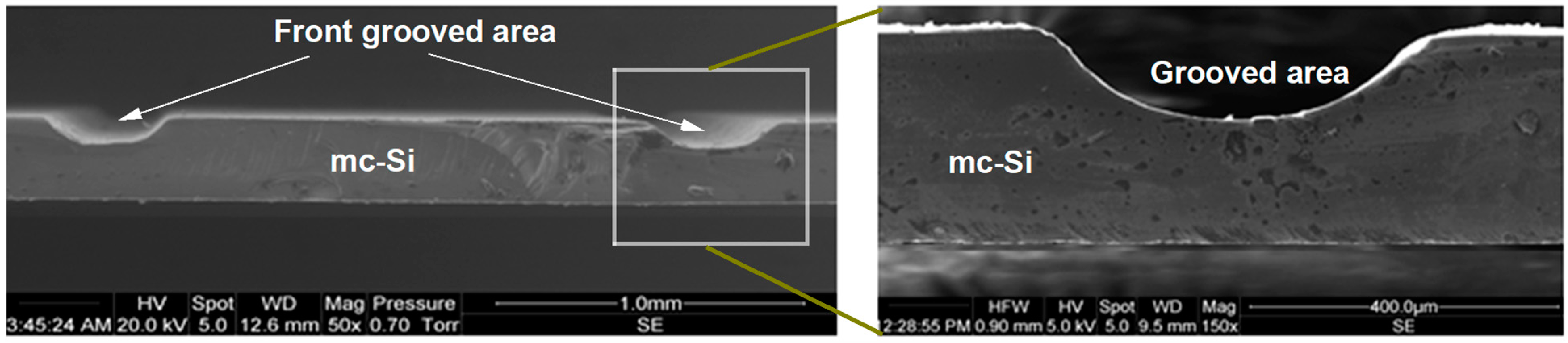
The depths of the etched patterns play a significant role in the manufacture of solar cells. In order to evaluate the sample thickness accurately and directly, laboratory measurements were taken using Fourier-transform infrared spectroscopy (FTIR). To limit the area exposed to radiation, the sample was mounted to a diaphragm with a 2 mm square aperture on each side. The well-known “fringing effect” [
20,
21] results from the IR beam’s constructive and destructive interference with the prepared samples’ parallel surfaces, often through their smooth surfaces and parallel sides. The grooved sample’s FTIR spectrum, as shown in
Figure 2, clearly illustrates this effect.
Nevertheless, we used the following formula (Bragg’s law) to determine the grooved sample’s thickness based on this fringing effect:
In Equation (1), e is the etched thickness of the silicon wafer, n is the refractive index, N is the number of fringes in a particular spectral region, and i and j are the start and end points of the spectrum, respectively, in cm−1.
Despite the fact that the silicon’s refractive index n changes with wavelength, it tends to be 3.42 [
22] for the longer wavelengths where the transmission peaks are the highest.
We chose start (i) and end (j) points in the spectral ranges of 3010.384 and 2919.745 cm
−1, respectively, based on the spectrum depicted in
Figure 3 and we calculated the total number of fringes throughout this spectrum region as 6. We then chose the spectrum’s start and end points as its minima and maxima, respectively, and then tallied the number of opposite minima or maxima. In this case, if we chose minima values for the spectrum’s start and end points, we also chose maxima points to determine how many fringes there were. On entering these numbers into our calculation, we determined the sample thickness of the grooved area to be 96.77 microns. This computed value compared favorably with the anticipated thickness of the silicon wafer, and an example of the grooved area in mc-Si is shown in
Figure 3, obtained by the CV etching method.
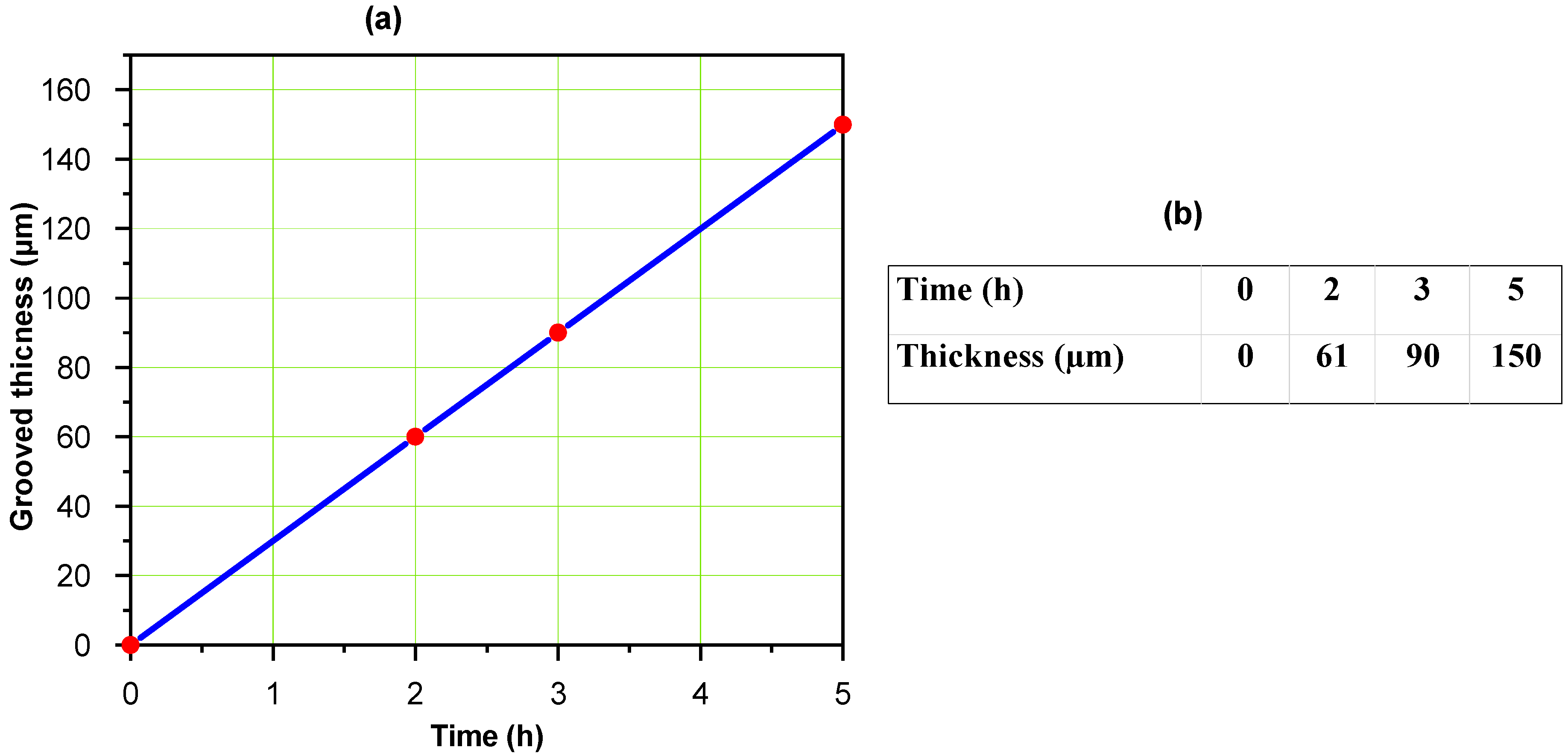
The observed experimental law e = f(t) represents the variation in the etched thickness (e) over time (t) during the etching process.
Figure 4a shows the linear dependence of the curve e = f(t), meaning that the etched thickness increases linearly over time during the etching reaction. It also suggests that the etching process follows a constant etch rate with a fixed amount of material being removed in a set unit of time. Such linear behavior can occur under certain etching conditions and mechanisms, such as when the etching rate is primarily determined by a diffusion-controlled process. The linear dependence observed in
Figure 4a provides some valuable information for understanding the kinetics of the etching reaction, and it allows researchers to calculate the etch rate, which is the rate at which the material is being removed. In turn, this helps to predict the thickness of the material at different points in the etching process. In our case, the etch rate was approximately 30 microns per hour, as shown in
Figure 4b. Two factors mainly make this process a linear one, namely (i) the nature of the layer formed, which is so porous that it provides no protection to the silicon substrate against contact with acid vapors, and (ii) the concentration of the stock solution, which remains virtually unchanged during the etching process thanks to its long life. Having this linear relationship between etched thickness and time is advantageous in certain applications. In the semiconductor and microfabrication sectors, the etching process’ linear reliance on time is useful for obtaining precision and reproducibility. It offers a simple and dependable way to manage the etching depth and, consequently, the size and characteristics of produced structures and devices. Furthermore, for quality assurance, precise and repeatable etching is crucial. The use of linear etching techniques helps manufacturers in the semiconductor and microfabrication sectors achieve stringent norms and requirements.
The linear relationship between etched thickness and time, as demonstrated in
Figure 4a, suggests that it is possible to reasonably and precisely create grooves of different widths and depths on mc-Si. Indeed, this procedure enables grooves to be formed on mc-Si with a resolution of just a few micrometers. Such grooving is of interest due to its applications for manufacturing specific components in microelectronics, such as mc-Si solar cells with front deep contacts. In addition, the use of hemispherical grooves in applications like microelectronics engineering, micromachining, and buried metal contacts in solar cells offers several advantages. One such advantage is the ability to produce low-cost grooves on mc-Si, thus greatly reducing manufacturing costs and making these devices more accessible and affordable. Furthermore, the ability to control the groove depth based on three external parameters is a crucial feature of this technology. By adjusting these parameters, manufacturers can precisely control the depth of the grooves to meet their specific requirements. This in turn allows grooves to be customized for various applications while ensuring that the produced devices have the desired functionality and performance. These three external parameters are the solution temperature, substrate temperature, and acid vapor etching time, because they all directly influence the etching rate and depth of the grooves. By carefully adjusting these parameters, manufacturers can create grooves with precise depths, shapes, and dimensions for their intended application. Overall, the opportunity for low-cost production while ensuring precise control over groove depth makes this technology attractive for its potential to achieve innovative designs and enhanced functionality for a wide range of devices. It could, therefore, drive advancements in microfabrication and semiconductor technologies and offer sustainable development.
3. Results and Discussion
To ensure that the results of the solar cell were comparable before and after the CV etching, the wafers used in the study needed to have sufficiently similar properties, including a crystal distribution and impurity content. Thus, the wafers used in this study were consecutively cut from the same bricks, also known as twin wafers. These wafers were p-type mc-Si with a resistivity of 0.5–2 Ω.cm, dimensions of 5 cm × 5 cm, and a thickness of 330 µm. After cutting the mc-Si, the wafers were cleaned with an acid solution to eliminate any metallic traces and surface defects that resulted from the cutting operation [
23]. On cleaning the mc-Si samples, a diode structure needed to be created to prepare them for solar cell fabrication [
24]. This involved doping the mc-Si samples with phosphorus using the spin-on method, which entailed depositing a few drops of a POCl
3 solution diluted in acetone onto the mc-Si wafer to achieve a uniform layer before drying the samples on a hot plate at 250 °C for 2 min. Over this time, vapors were released due to the combustion of organic solvents. To facilitate the effective diffusion of phosphorus, the samples were positioned vertically on a quartz boat inside an oven with a controlled gaseous atmosphere which included oxygen and nitrogen. The manufacturing process and the quantity of pre-deposited POCl
3 have a significant influence on the performance of mc-Si solar cells. The wafers were maintained at a temperature of 925 °C for 30 min under a flow of nitrogen. The pre-deposited POCl
3 decomposed under the effect of oxygen according to the following reactions:
The doping phosphorus penetrated further depending upon the temperature, resulting in a completed n–p junction. To connect the n–p junction to the external circuit for use, we needed to construct ohmic contacts at the terminals of the junction, something that is achieved when the selected metal forms an ohmic contact with the mc-Si substrate. This metallization was achieved using the screen printing technique. The most commonly used technique for this is sputtering for several reasons. First, it offers an advantageous price thanks to a low loss of time and materials when compared to thermal evaporation, and it enables a large production capacity at speed. The rear surface contact was formed from a specially made silver/aluminum alloy that had been designed for solar cells, because adding silver ensures good weldability. Once the metal layer masked the rear surface of the cell without touching the edges, the cell was then annealed at a temperature of 850 °C. Both the drying and annealing were performed in an infrared furnace. Thanks to the high annealing temperature, the aluminum diffused, causing the rear face of the substrate to become heavily doped (P+), leading to an increased Vco due to the presence of an additional P–P+ rear barrier. The front contact was made using a silver paste specifically designed for solar cells, with the geometric shape and dimensions of the grid being chosen to achieve a low coverage rate. The silver paste was then annealed at a temperature of 720 °C. Annealing at higher temperatures was avoided for two reasons: (i) to minimize the risk of the contact penetrating into the N layer, which could in turn result in the contact reaching the P zone due to the thinness of the N zone and increase the risk of a short circuit, and (ii) to protect the cell from being contaminated by the aluminum vapors released during the annealing of the rear face.
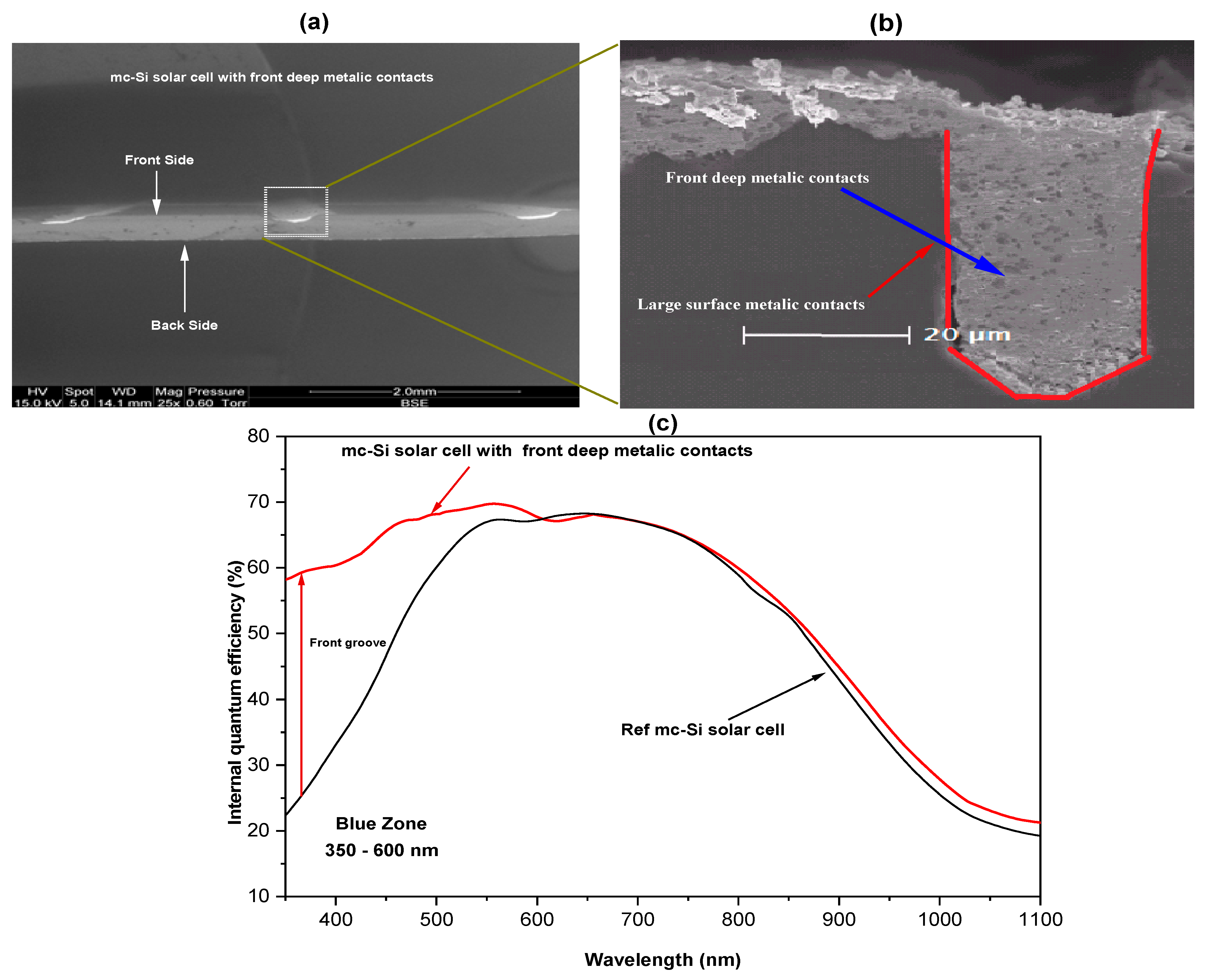
Assessing the direct effect of grooves on carrier generation and collection efficiency can be achieved in a clear and quantitative manner by comparing the IQE of multicrystalline silicon solar cells with and without front deep contacts. This method could inform further study and innovation in solar cell design, and it is a crucial step in comprehending the possible significance of grooves for increasing cell performance. This study therefore sheds some important light on how grooves affect solar cell performance, particularly in terms of their potential to increase overall cell efficiency. Indeed, using front deep contacts is a valuable approach for enhancing the performance of multicrystalline silicon (mc-Si) solar cells, because they offer a specialized electrode configuration that optimizes charge carrier collection and reduces recombination losses (see
Figure 5 and
Figure 6). More specifically, the interlocking finger-like structures of the contacts on the front surface of the cell create shorter pathways for charge carriers to travel to their respective contacts, thus minimizing the overall distance they need to traverse and reducing the chance of a charge carrier recombining within the silicon material.
In fact, we did not treat the surface because the silicon surface exposed to solar radiation was not treated, but we compared two solar cells before and after buried metal contact. That is, the first cell is shown in
Figure 5a with the metal contact form on its surface, while the second cell shown in
Figure 5b has the buried metal contact form in the depth of the cell, as shows in
Figure 5.
The buried contact solar cell refers to the silicon solar cell in which the metal was buried in the formed groove inside of it.
Solar cells with buried metal contacts (
Figure 5b) improve charge carrier extraction by providing larger contact surfaces and reducing the distance traveled by the carriers compared to the simple contact model (
Figure 5a) with small contact surfaces and a large distance traveled by the carriers. In photovoltaic cells, carriers generated by incident light need to travel across a large distance within the semiconductor material to reach the metal contacts. If there is significant recombination along this path, it can reduce the overall efficiency of the solar cell. When carriers have to travel over a large distance within the semiconductor and encounter small contact surfaces, there is a higher probability of recombination events occurring, Thus, a solar cell with a buried metal contact (
Figure 5b) increases the collection area, reduces contact resistance, and has a low probability of recombination, resulting in improved solar cell efficiency.
The measurements of the internal quantum efficiency (IQE) as a function of the wavelength of the mc-Si solar cell, before and after having front deep contacts, are shown in
Figure 6.
Figure 6c shows the quantum efficiency of a reference mc-Si solar cell compared to that of a mc-Si solar cell with front deep contacts. It can be seen how the addition of front-buried metallic contacts affects the quantum efficiency of mc-Si solar cells in the 350 nm to 600 nm wavelength range by reducing the effective thickness of the cell. This leads to an increase in the collection probability of minority carriers at short wavelengths (350–600 nm), thus enhancing the quantum efficiency of the mc-Si solar cell in this spectral region (Blue Zone in
Figure 6c). Indeed, the quantum efficiency of mc-Si solar cells can be enhanced by up to 35% in the short wavelength range. A thinner base width combined with front deep contacts facilitates more efficient charge carrier extraction by providing larger contact surfaces and reducing travel distances for carriers, as shown by the red line in
Figure 6b. This optimization positively affects cell performance and quantum efficiency, resulting in greater efficiency and better overall performance for the mc-Si solar cell. The results obtained here surpass those obtained through front silicon solar cell passivation [
25,
26,
27,
28] and are comparable to those reported in other studies [
29,
30,
31,
32,
33].
In summary, front deep contacts enhance mc-Si solar cell performance by improving carrier collection in response to sunlight [
34], while the interlocking fingers facilitate the quick and effective transport of carriers to the contacts. In addition, recombination losses are reduced thanks to the shorter carrier pathways, thus contributing to a higher overall energy conversion efficiency. What is more, the finger-like structures of front deep contacts minimize shadowing effects (see in
Figure 6a), thus allowing more incident light to reach the cell’s surface and increasing the potential for light absorption. This can lead to the internal quantum efficiency improving for shorter wavelengths, thus enabling sunlight to be converted into usable electrical energy more easily [
35,
36].


 ,
, 