
Design and Performance Evaluation of a Step-Up DC–DC Converter with Dual Loop Controllers for Two Stages Grid Connected PV Inverter


Abstract
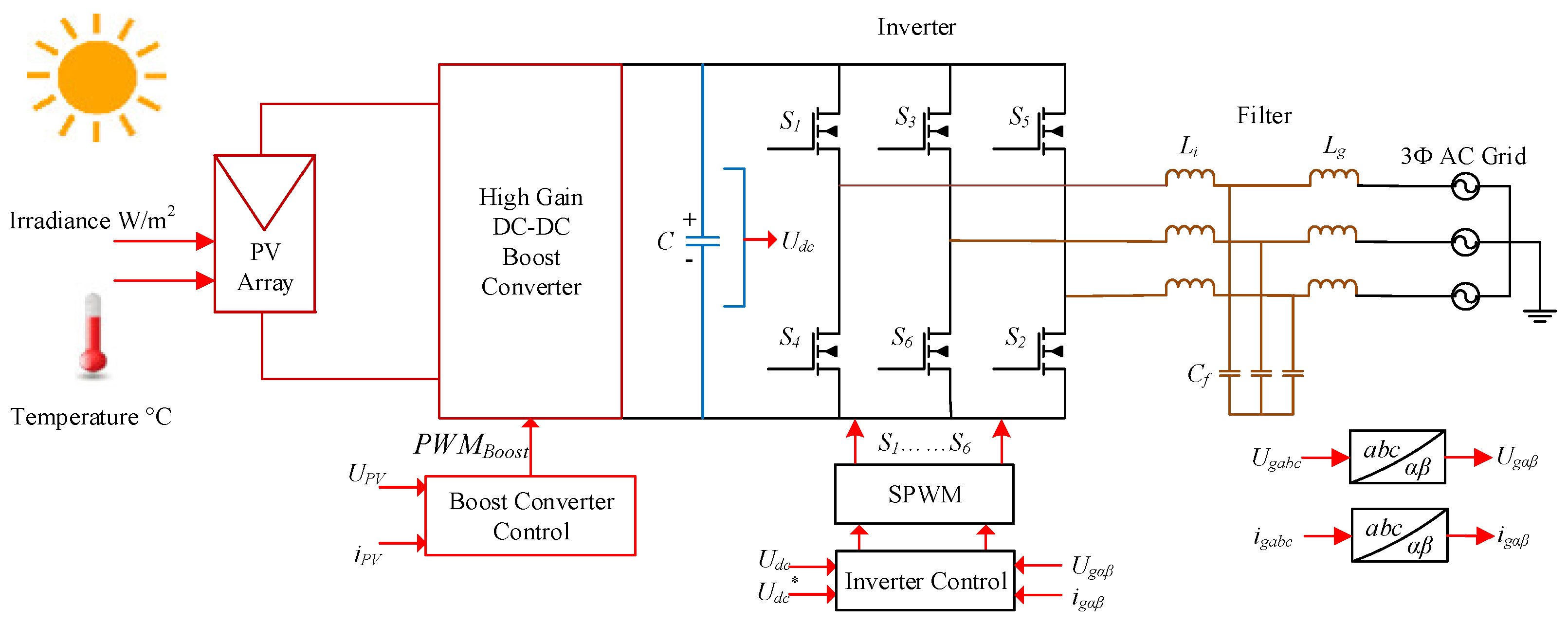
:1. Introduction
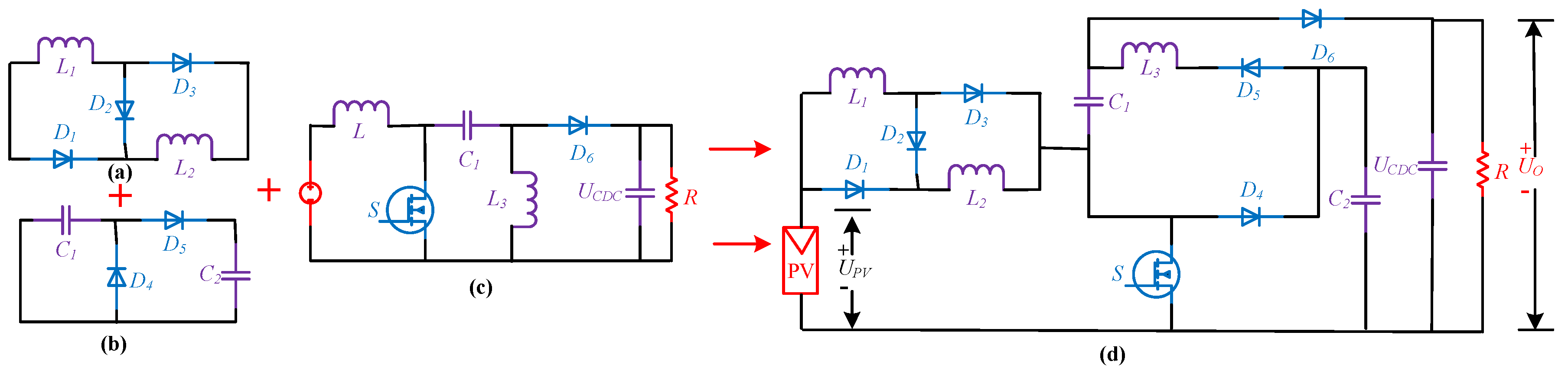
- A transformer-less high voltage gain DC–DC converter is presented that extracts the maximum power from the PV panel by using Perturb and Observe (P&O) MPPT technique and step-up the low generated PV voltage to a level applicable for grid connected PV inverter. In the proposed topology, a voltage doubler circuit and switch inductor cell are integrated with the SEPIC converter to attain a high voltage conversion ratio. The prominent features of the converter include single switch, simple control, low voltage stress, high efficiency, and fewer components.
- Back propagation algorithm-based API and AFOPI controllers are designed to regulate a DC-link voltage in case of PV intermittency. This adaptive scheme enhances the system performance and handles the system uncertainties by dynamically updating the control law parameters. The proposed controllers have a faster dynamic response and easy implementation, which improves the system stability.
- Based on the Naslin polynomial method, a PR controller is designed, considering the dynamic behavior of an LCL filter. In the proposed controller, no parameter is computed empirically or by trial-and-error method. To show the effectiveness of the controller, it is implemented in a 3Φ grid-connected PV system that results in low THD.
2. Analysis of DC–DC Converter
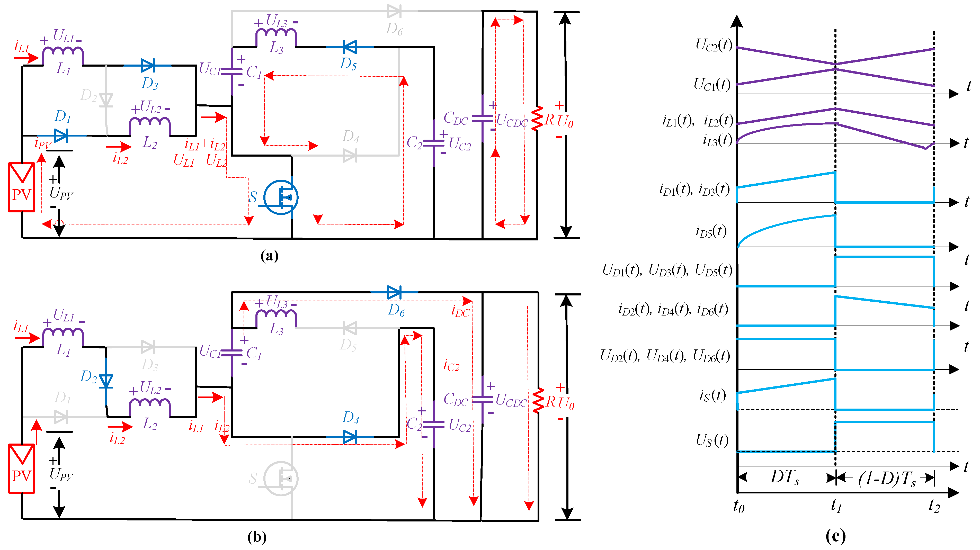
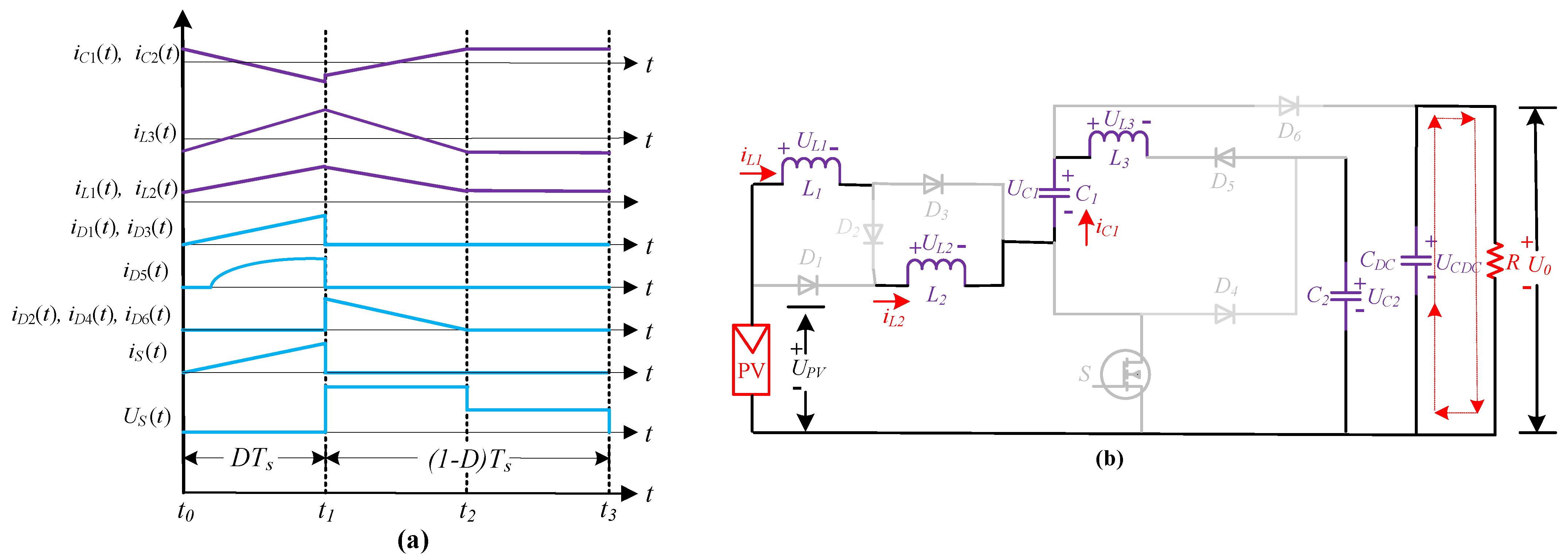
2.1. Proposed Converter Topology and Operating Modes
2.1.1. Continuous Conduction Mode
- Switching Interval (t0 ~ t1)
- Switching Interval (t1 ~ t2)
2.1.2. Discontinuous Conduction Mode
- Switching Interval (t0 ~ t1)
- Switching Interval (t1 ~ t2)
- Switching Interval (t2 ~ t3)
2.2. Performance Evaluation of Converter
2.2.1. Voltage Gain Derivation
2.2.2. Voltage Stress Calculation
2.2.3. Design of Inductors and Capacitors
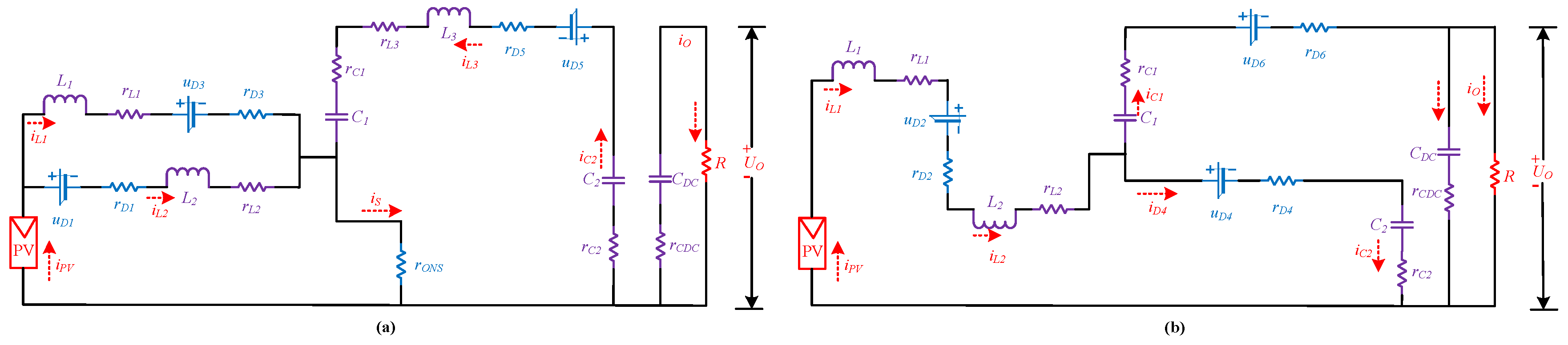
2.2.4. Loss Analysis
- Inductor Copper Loss
- Capacitor Loss
- Switch Loss
- Diode Loss
- Total Loss
2.2.5. Comparative Analysis
3. Inverter Controller Design
3.1. DC-Link Voltage Regulation
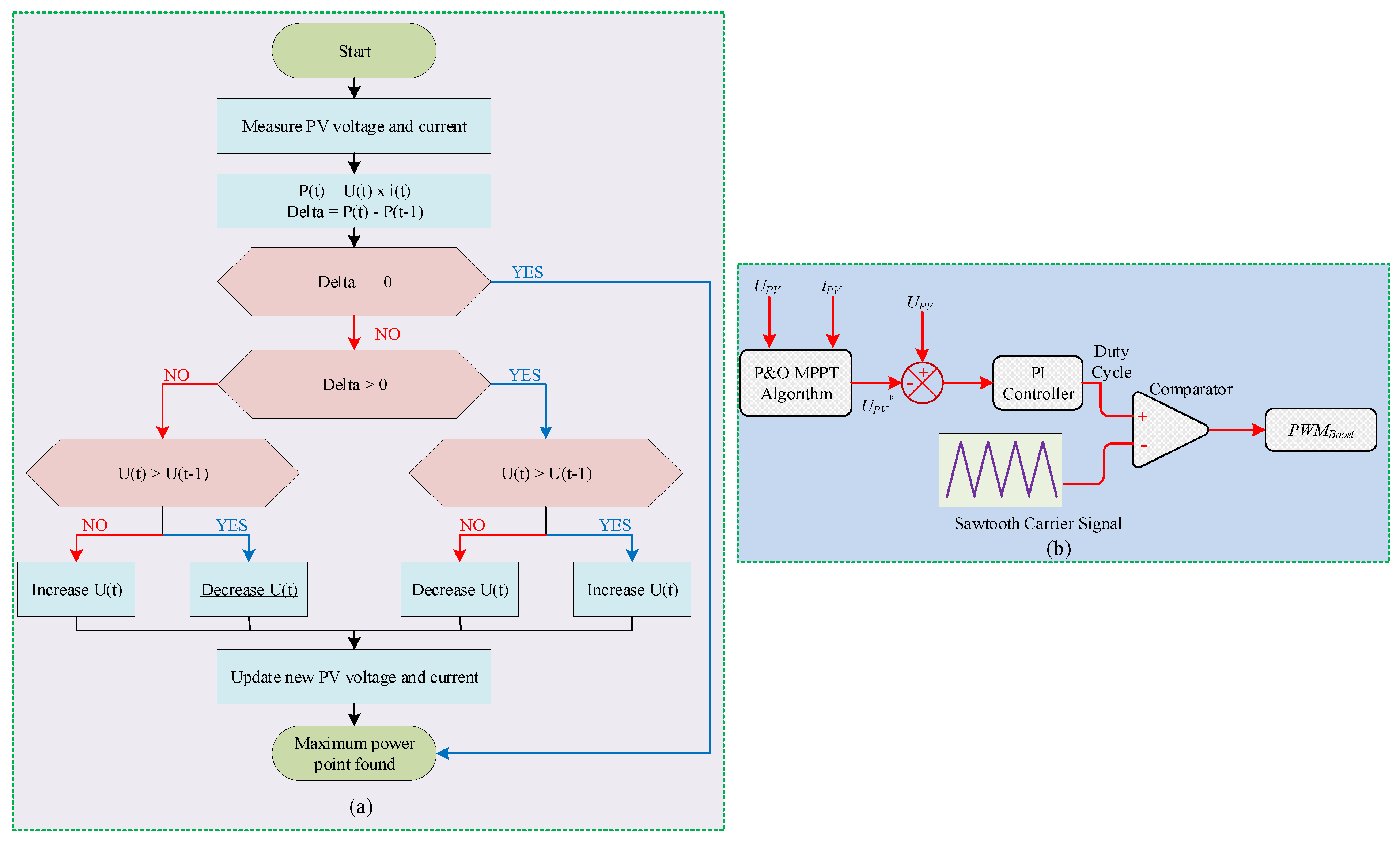
3.1.1. Adaptive PI Controller
3.1.2. Adaptive FOPI Controller
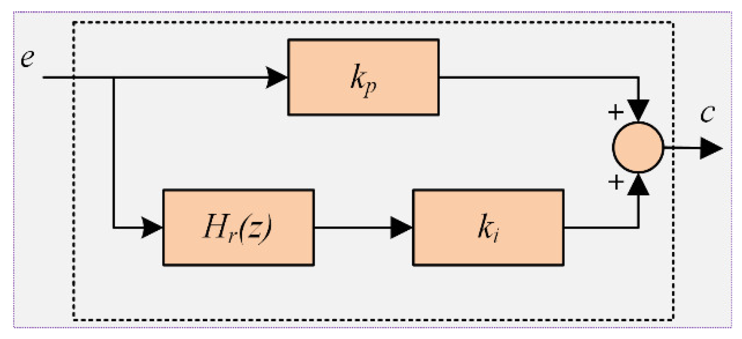
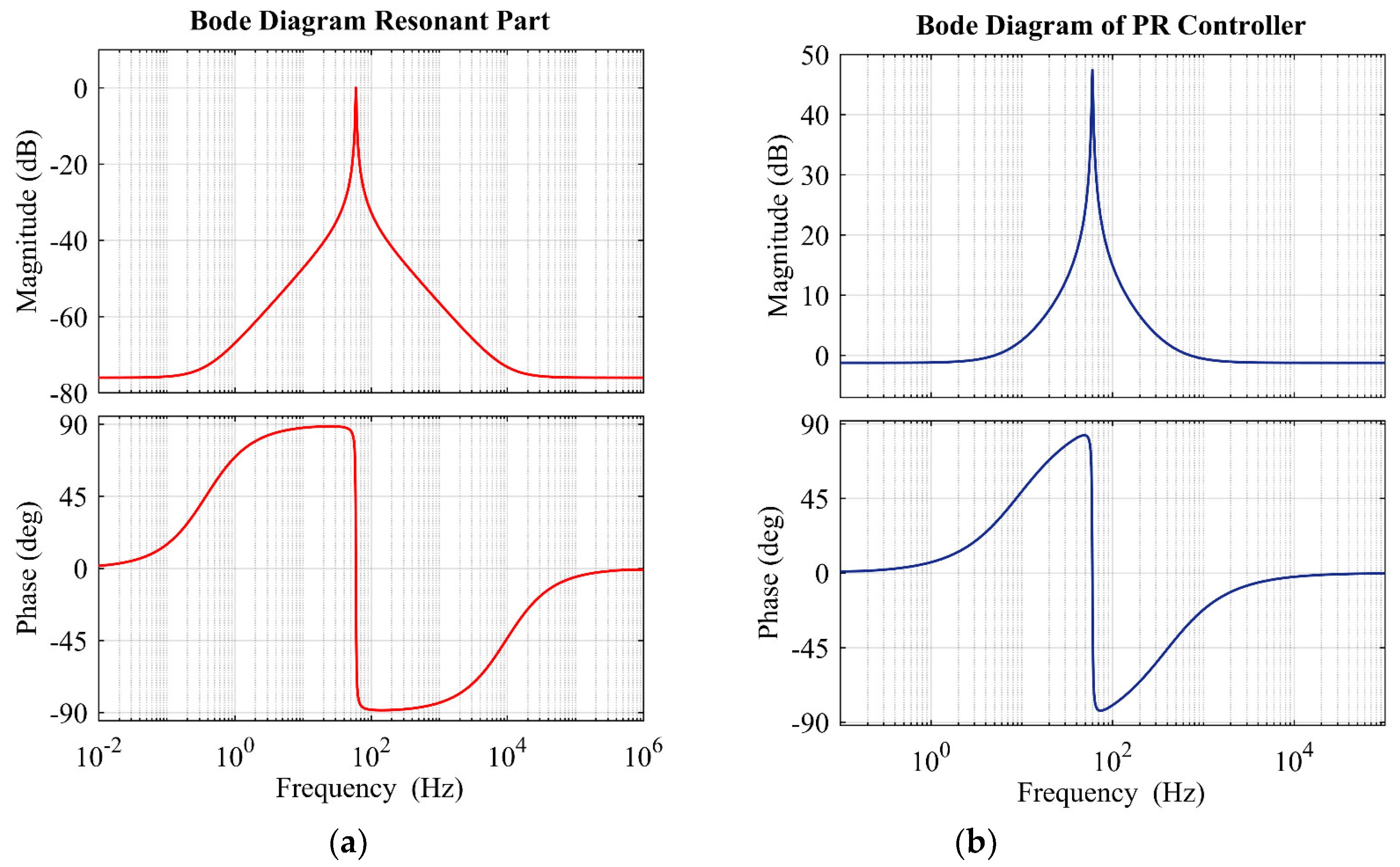
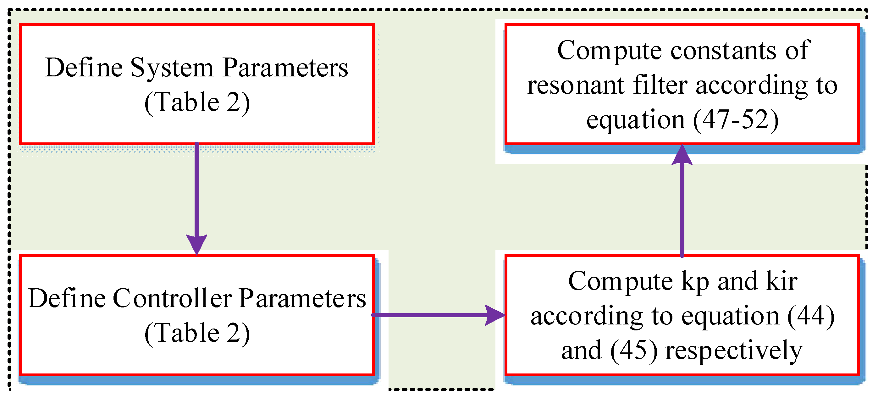
3.2. Current Controller
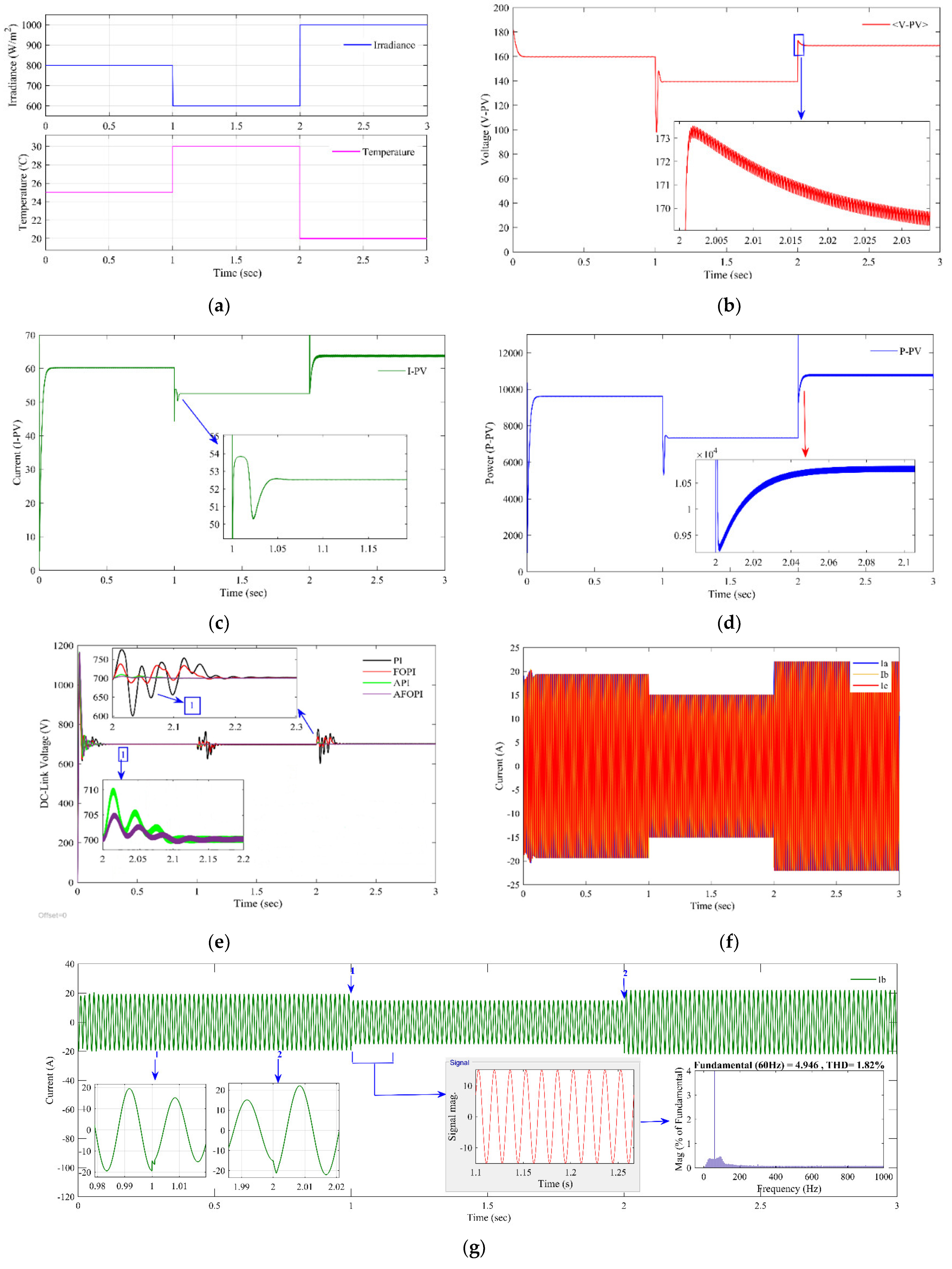
4. Results and Discussion
4.1. Simulation Results of DC–DC Converter
4.2. Simulation Results of Overall PV System
5. Conclusions
Author Contributions
Funding
Institutional Review Board Statement
Informed Consent Statement
Data Availability Statement
Conflicts of Interest
Appendix A

| Parameter | Symbol | Value |
|---|---|---|
| Voltage at MPP | VMPP | 29.9 V |
| Current at MPP | IMPP | 7.65 A |
| Nominal power | PMPP | 228 W |
| Open circuit voltage | UOC | 37.1 V |
| Short circuit current | ISC | 8.18 A |
| Controller | Parameter | Value |
|---|---|---|
| Controller of Boost Converter | ||
| PI | kp | 0.01 |
| ki | 0.5 | |
| DC-Link Voltage Controller | ||
| PI | kp | 32 |
| ki | 210 | |
| FOPI | kp | 17 |
| ki | 105 | |
| λ | 0.715 | |
| API | kp | 8 |
| ki | 23 | |
| γ | 400 | |
| AFOPI | kp | 18 |
| ki | 145 | |
| λ | 0.545 | |
| γ | 230 | |
| Current Controller | ||
| PR | Kp | 7.074702865475842 |
| Ki | 5.716971169217982 | |
| a0 | 1 | |
| a1 | −1.999990433144820 | |
| a2 | 0.999990575266452 | |
| b0 | 9.424777960769379 × 10⁻⁶ | |
| b1 | −9.424777291035913 × 10⁻⁶ | |
| b2 | 0 | |
| C | 4.441300946117881 × 10⁻⁵ | |
References
- Khan, M.Y.A.; Liu, H.; Rehman, N.U. Design of a Multiport Bidirectional DC–DC Converter for Low Power PV Applications. In Proceedings of the 2021 International Conference on Emerging Power Technologies (ICEPT), Topi, Pakistan, 10–11 April 2021; pp. 1–6. [Google Scholar]
- Ali Khan, M.Y.; Liu, H.; Yang, Z.; Yuan, X. A Comprehensive Review on Grid Connected Photovoltaic Inverters, Their Modulation Techniques, and Control Strategies. Energies 2020, 13, 4185. [Google Scholar] [CrossRef]
- Das, M.; Pal, M.; Agarwal, V. Novel high gain, high efficiency dc–dc converter suitable for solar PV module integration with three-phase grid tied inverters. IEEE J. Photovolt. 2019, 9, 528–537. [Google Scholar] [CrossRef]
- Habib, S.; Khan, M.M.; Abbas, F.; Ali, A.; Faiz, M.T.; Ehsan, F.; Tang, H. Contemporary trends in power electronics converters for charging solutions of electric vehicles. CSEE J. Power Energy Syst. 2020, 6, 911–929. [Google Scholar]
- Pop-Calimanu, I.-M.; Lica, S.; Popescu, S.; Lascu, D.; Lie, I.; Mirsu, R. A new hybrid inductor-based boost DC–DC converter suitable for applications in photovoltaic systems. Energies 2019, 12, 252. [Google Scholar] [CrossRef] [Green Version]
- Sanjeevikumar, P.; Bhaskar, M.S.; Dhond, P.; Blaabjerg, F.; Pecht, M. Non-isolated sextuple output hybrid triad converter configurations for high step-up renewable energy applications. In Advances in Power Systems and Energy Management; Springer: Berlin/Heidelberg, Germany, 2018; pp. 1–12. [Google Scholar]
- Almalaq, Y.; Matin, M. Two-Switch High Gain Non-Isolated Cuk Converter. Eng. Technol. Appl. Sci. Res. 2020, 10, 6362–6367. [Google Scholar] [CrossRef]
- Banaei, M.R.; Sani, S.G. Analysis and implementation of a new SEPIC-based single-switch buck–boost DC–DC converter with continuous input current. IEEE Trans. Power Electron. 2018, 33, 10317–10325. [Google Scholar] [CrossRef]
- Zhang, G.; Iu, H.H.-C.; Zhang, B.; Li, Z.; Fernando, T.; Chen, S.-Z.; Zhang, Y. An impedance network boost converter with a high-voltage gain. IEEE Trans. Power Electron. 2017, 32, 6661–6665. [Google Scholar] [CrossRef]
- Ma, M.; Liu, X.; Lee, K.Y. Maximum Power Point Tracking and Voltage Regulation of Two-Stage Grid-Tied PV System Based on Model Predictive Control. Energies 2020, 13, 1304. [Google Scholar] [CrossRef] [Green Version]
- Lakshmi, M.; Hemamalini, S. Decoupled control of grid connected photovoltaic system using fractional order controller. Ain Shams Eng. J. 2018, 9, 927–937. [Google Scholar] [CrossRef] [Green Version]
- Asadi, M.; Ebrahimirad, H.; Mousavi, M.; Jalilian, A. Sliding mode control of DC-link capacitors voltages of a NPC 4-wire shunt active power filter with selective harmonic extraction method. In Proceedings of the 2016 7th Power Electronics and Drive Systems Technologies Conference (PEDSTC), Tehran, Iran, 16–18 February 2016; pp. 273–278. [Google Scholar]
- Kumar, N.B.; Urundady, V. Sliding Mode Controller with Integral Action for DC-Link Voltage Control of Grid-Integrated Domestic Photovoltaic Systems. Arab. J. Sci. Eng. 2020, 45, 6583–6600. [Google Scholar] [CrossRef]
- Zeb, K.; Islam, S.U.; Din, W.U.; Khan, I.; Ishfaq, M.; Busarello, T.D.C.; Ahmad, I.; Kim, H.J. Design of fuzzy-PI and fuzzy-sliding mode controllers for single-phase two-stages grid-connected transformerless photovoltaic inverter. Electronics 2019, 8, 520. [Google Scholar] [CrossRef] [Green Version]
- Bielskis, E.; Baskys, A.; Valiulis, G. Controller for the grid-connected microinverter output current tracking. Symmetry 2020, 12, 112. [Google Scholar] [CrossRef] [Green Version]
- Zhang, N.; Tang, H.; Yao, C. A systematic method for designing a PR controller and active damping of the LCL filter for single-phase grid-connected PV inverters. Energies 2014, 7, 3934–3954. [Google Scholar] [CrossRef]
- Busarello, T.D.C.; Pomilio, J.A.; Simoes, M.G. Design procedure for a digital proportional-resonant current controller in a grid connected inverter. In Proceedings of the 2018 IEEE 4th Southern Power Electronics Conference (SPEC), Singapore, 10–13 December 2018; pp. 1–8. [Google Scholar]
- Yagnik, U.P.; Solanki, M.D. Comparison of L, LC & LCL filter for grid connected converter. In Proceedings of the 2017 International Conference on Trends in Electronics and Informatics (ICEI), Tirunelveli, India, 11–12 May 2017; pp. 455–458. [Google Scholar]
- Mao, M.; Cui, L.; Zhang, Q.; Guo, K.; Zhou, L.; Huang, H. Classification and summarization of solar photovoltaic MPPT techniques: A review based on traditional and intelligent control strategies. Energy Rep. 2020, 6, 1312–1327. [Google Scholar] [CrossRef]
- Waly, H.M.; Osheba, D.S.; Azazi, H.Z.; El-Sabbe, A.E. Design and analysis of a proposed transformerless/non-isolated high- gain DC–DC converter for renewable energy applications. Int. J. Electron. 2020, 107, 1127–1145. [Google Scholar] [CrossRef]
- Biricik, S.; Redif, S.; Khadem, S.K.; Basu, M. Improved harmonic suppression efficiency of single-phase APFs in distorted distribution systems. Int. J. Electron. 2016, 103, 232–246. [Google Scholar] [CrossRef]
- Jiao, Y.; Luo, F.; Zhu, M. Voltage-lift-type switched-inductor cells for enhancing DC–DC boost ability: Principles and integrations in Luo converter. IET Power Electron. 2011, 4, 131–142. [Google Scholar] [CrossRef]
- Tang, Y.; Fu, D.; Wang, T.; Xu, Z. Hybrid switched-inductor converters for high step-up conversion. IEEE Trans. Ind. Electron. 2014, 62, 1480–1490. [Google Scholar] [CrossRef]
- Almalaq, Y.; Matin, M. Three topologies of a non-isolated high gain switched-inductor switched-capacitor step-up cuk converter for renewable energy applications. Electronics 2018, 7, 94. [Google Scholar] [CrossRef] [Green Version]
- Sedaghati, F.; Azizkandi, M.E.; Majareh, S.H.L.; Shayeghi, H. A high-efficiency non-isolated high-gain interleaved DC–DC converter with reduced voltage stress on devices. In Proceedings of the 2019 10th International Power Electronics, Drive Systems and Technologies Conference (PEDSTC), Shiraz, Iran, 12–14 February 2019; pp. 729–734. [Google Scholar]
- Banaei, M.R.; Bonab, H.A.F. A novel structure for single-switch nonisolated transformerless buck–boost DC–DC converter. IEEE Trans. Ind. Electron. 2016, 64, 198–205. [Google Scholar] [CrossRef]
- Zeb, K.; Nazir, M.S.; Ahmad, I.; Uddin, W.; Kim, H.-J. Control of Transformerless Inverter-Based Two-Stage Grid-Connected Photovoltaic System Using Adaptive-PI and Adaptive Sliding Mode Controllers. Energies 2021, 14, 2546. [Google Scholar] [CrossRef]
- Haroon, Z.; Khan, B.; Farid, U.; Ali, S.; Mehmood, C. Switching control paradigms for adaptive cruise control system with stop-and-go scenario. Arab. J. Sci. Eng. 2019, 44, 2103–2113. [Google Scholar] [CrossRef]
- Bacha, S.; Munteanu, I.; Bratcu, A.I. Linear Control Approaches for DC–AC and AC–DC Power Converters. In Power Electronic Converters Modeling and Control; Springer: Berlin/Heidelberg, Germany, 2014; pp. 237–296. [Google Scholar]


| Topology | Switches | Diodes | Inductors | Capacitors | Passive | Total | Voltage Gain | Voltage Stress on Switch |
|---|---|---|---|---|---|---|---|---|
| Cuk, SEPIC, Zeta | 1 | 1 | 2 | 2 | 4 | 6 | ||
| [6] | 1 | 7 | 4 | 2 | 6 | 14 | ||
| [8] | 1 | 3 | 4 | 6 | 10 | 14 | ||
| [22] | 2 | 5 | 3 | 4 | 7 | 14 | ||
| [23] | 2 | 7 | 4 | 1 | 5 | 14 | ||
| [24] | 1 | 8 | 4 | 3 | 7 | 16 | ||
| [25] | 2 | 4 | 4 | 6 | 10 | 16 | ||
| [26] | 1 | 3 | 3 | 5 | 8 | 12 | ||
| Proposed | 1 | 6 | 3 | 3 | 6 | 13 |
| Parameter | Value |
|---|---|
| Grid Voltage (Ug) | 230 V rms |
| Grid frequency (fg) | 60 Hz |
| Converter-side inductor (Li) | 1.74 × 10⁻⁴ H |
| Converter-side resistance (Ri) | 0.01 ohm |
| Grid-side inductor (Lg) | 1.2 × 10⁻³ H |
| Grid-side resistance (Rg) | 0.01 ohm |
| LCL capacitance (Cf) | 3.31 × 10⁻⁵ F |
| LCL damping resistance (Rd) | 20.5 ohm |
| DC-link voltage (UDC) | 700 V |
| Grid resistance (Rs) | 2 ohm |
| Grid inductance (Ls) | 3 × 10⁻³ H |
| Switching frequency (fsw) | 10 × 10−3 Hz |
| Sampling frequency (fa) | 1/1 × 10−6 Hz |
| Sampling period (Ta) | 1 × 10⁻⁶ s |
| Resonant frequency (fr) | 60, 300 Hz |
| Resonant frequency bandwidth (Bs) | 1.5 |
| Resonant angular bandwidth (Br) | Br = 2πBs |
| Resonant gain (kr) | 1 |
| Damping factor (ζ) | 0.95 |
| Components | Values |
|---|---|
| Input Voltage | 70 V |
| Output Voltage | 705 V |
| Inductors (L1 and L2) | 205 × 10−6 H |
| Inductor (L3) | 180 × 10−6 H |
| Capacitors (C1 and C2) | 2.2 × 10⁻⁶ F |
| Capacitor (CDC) | 450 × 10−6 F |
| Duty Cycle | 71% |
| Switching Frequency | 24 kHz |
| Load Resistance | 100 Ω |
Publisher’s Note: MDPI stays neutral with regard to jurisdictional claims in published maps and institutional affiliations. |
© 2022 by the authors. Licensee MDPI, Basel, Switzerland. This article is an open access article distributed under the terms and conditions of the Creative Commons Attribution (CC BY) license (https://creativecommons.org/licenses/by/4.0/).
Share and Cite
Khan, M.Y.A.; Liu, H.; Habib, S.; Khan, D.; Yuan, X. Design and Performance Evaluation of a Step-Up DC–DC Converter with Dual Loop Controllers for Two Stages Grid Connected PV Inverter. Sustainability 2022, 14, 811. https://doi.org/10.3390/su14020811
Khan MYA, Liu H, Habib S, Khan D, Yuan X. Design and Performance Evaluation of a Step-Up DC–DC Converter with Dual Loop Controllers for Two Stages Grid Connected PV Inverter. Sustainability. 2022; 14(2):811. https://doi.org/10.3390/su14020811
Chicago/Turabian StyleKhan, Muhammad Yasir Ali, Haoming Liu, Salman Habib, Danish Khan, and Xiaoling Yuan. 2022. "Design and Performance Evaluation of a Step-Up DC–DC Converter with Dual Loop Controllers for Two Stages Grid Connected PV Inverter" Sustainability 14, no. 2: 811. https://doi.org/10.3390/su14020811
APA StyleKhan, M. Y. A., Liu, H., Habib, S., Khan, D., & Yuan, X. (2022). Design and Performance Evaluation of a Step-Up DC–DC Converter with Dual Loop Controllers for Two Stages Grid Connected PV Inverter. Sustainability, 14(2), 811. https://doi.org/10.3390/su14020811