Article

Modeling and Application of Controllers for a Photovoltaic Inverter for Operation in a Microgrid

by
Rubén Ortega
1,
Víctor H. García
1,
Adrián L. García-García
2,
Jaime J. Rodriguez
3,
Virgilio Vásquez
4 and
Julio C. Sosa-Savedra
2,*
1
Instituto Politécnico Nacional, Escuela Superior de Cómputo (ESCOM), Ciudad de México 07738, Mexico
2
Instituto Politécnico Nacional, Centro de Investigación en Ciencia Aplicada y Tecnología Avanzada, Santiago de Querétaro 76090, Mexico
3
Instituto Politécnico Nacional, Escuela Superior de Ingeniería Mecánica y Eléctrica (ESIME), Ciudad de México 07340, Mexico
4
Instituto Tecnológico y de Estudios Superiores de Monterrey, Campus Estado de México, Ciudad López Mateos 52926, Mexico
*
Author to whom correspondence should be addressed.
Sustainability 2021, 13(9), 5115; https://doi.org/10.3390/su13095115
Submission received: 29 September 2020 / Revised: 11 December 2020 / Accepted: 12 December 2020 / Published: 3 May 2021
(This article belongs to the Special Issue Sustainable Conversion of Renewable Energy Sources)

Abstract

:
The penetration of renewable energies in the context of distributed generation represents challenges such as maintaining the reliability and stability of the system and considering the random behavior proper of generation and consumption. In this context, microgrids make it possible to manage effectively the generation and consumption of this energy, incorporating, electronic power converters, energy storage systems, and hierarchical control schemes. This paper presents the modeling, design, and application of controllers for a photovoltaic inverter operating in island mode. For this application, the photovoltaic inverter regulates the inverter output voltage via two control configurations implemented to follow the voltage reference imposed by the scheme droop. The first control scheme is configured with a two-degrees-of-freedom controller plus a repetitive controller. In this configuration, the repetitive controller is implemented in the direct loop. The second scheme is configured with an integral proportional controller—proportional controller plus a resonant controller. This configuration is formed by an integral proportional control in the direct loop plus a resonant controller and a proportional controller in the feedback loop. Both control configurations are implemented to improve the inverter disturbance rejection capability when it feeds both linear and non-linear local loads. In addition, these configurations allow the parallel connection of inverters with good performance, using a droop scheme that allows the parallel connection of converters. The tests are carried out by means of simulations using PSIMTM, which shows that, with the implemented controllers, the total harmonic distortion of the inverter output is below 5%, as recommended by the IEEE 519-1992 standard.

1. Introduction

Centralized generation is still the most common means of power generation and delivery worldwide. It is based on large facilities such as nuclear, hydro-, and thermo-electric power plants, interconnected through a network of high-voltage transmission lines that delivers power unidirectionally to distant end users in densely populated areas. By the same token, isolated, distant communities lack access to this utility due to elevated delivery cost. For these locations, distributed generation (DG) based on renewable energy sources (RES) is a better alternative, because generation takes place at or near the consumption point, lowering both generation and delivery costs [1]. In this case, it is possible to implement autonomous interfaces, able to control whether or not to connect to the utility grid, as physical or economic conditions dictate.
Microgrids [2,3,4], as they are known, consist of power converters and storage devices powered by a combination of RES like solar panels, fuel cells, and wind micro-turbines that require the use of power inverters to condition the amplitude, frequency, and shape of the voltage signal within standard requirements for harmonic control in electric power systems, regardless of applied load [5,6,7].
The diversity of RES able to mesh into microgrid power systems, as well as the need for effective and efficient management of both power generation and consumption, poses several challenges arising from the integration of electronic power converters, energy storage systems, and hierarchical control schemes. In particular, the control system must be capable of maintaining the energy balance in the microgrid, a complex task when the powers of the generation and consumption units are different [8]. Several approaches exist to address the integration issues caused by the inherent differences in the electrical characteristics of the microgrid elements. Thus, Baek, Cho, and Yeo (2019) propose a voltage control scheme with an inner repetitive current controller to achieve lower output impedance and better disturbance rejection capability for a UPS system, for which it is important to ensure the output voltage regulation and low total harmonic distortion (THD) under non-linear loads [9]. Jamil et al. (2020) developed a higher-order repetitive controller with phase lead compensator and applied it to the current control of a two-level three-phase grid-connected converter [10]. Jank et al. (2017) presented a comparative analysis of the PID, resonant, and repetitive controller applied to a single-phase half-bridge pulse-width modulation (PWM) inverter, varying the switching frequency and the inductor current ripple. They concluded that both switching frequency and inductor current ripple play a key role in the controller design [11]. Chen et al. (2020) designed a repetitive control for dual-buck full-bridge single-phase inverter to ensure the steady-state performance of the system, and adaptive PI control to speed up the system’s dynamic response process [12]. Chen et al. (2020) presented a PID-based repetitive control strategy to achieve high control accuracy for tracking a determined periodic reference signal [13]. Pan et al. (2018) developed a method to suppress current harmonic components caused by non-ideal factors. A new PID controller named R–2DOF PID controller was proposed and used in the control system of the permanent magnet synchronous linear motor (PMSLM) in the miniature microsecond laser cutting system, to suppress PMSLM current harmonics [14]. Patil and More (2019) compared the performance of a Cuk converter with proportional integral controller and a proportional resonant controller [15]. Sreekumar, Danthakani, and Veettil (2018) investigated the implementation of P-R controller in an autonomous DG unit [16]. Torres, Roncero-Sánchez, and Batlle (2018) developed a 2DOF resonant control scheme for voltage-sag compensation in dynamic voltage restorers [17]. Finally, Biricik and Komurcugil (2018) reported a control strategy for PUC inverters based on PI and PR controllers [18].
Other works present control methods to carry out parallel connection of the conversion units [19,20,21]. In [19], paralleling technique with VSI inverters is implemented. The RMS Current Control technique with droop in output voltage is implemented to inverter control. The LCL filter is used at inverter output for wave shaping and output reduced noise level output. The PI compensator is used in a feedback loop to attain the system stability. In [20], distributed generation units are connected to the microgrid through an interfacing inverter. The interfaced inverter plays the main role in the microgrid operating performance. In this paper, interfaced parallel inverter control using a droop control P-F/Q-V was investigated when the microgrid operated in island mode. In inverter islanding mode operation, droop control should maintain voltage and frequency stability. The droop control for parallel inverters is implemented and the proportional load sharing is obtained from each individual inverter. In [21], a control strategy is proposed to improve load sharing performance in order to reduce the circulating current between inverters parallel connected in microgrids in island mode operation. The control strategy includes a filter parameter estimator, which compensates for any possible uncertainty or deviation in its value. Double loop feedback control is also adopted, with external voltage and internal current control, providing excellent performance under transient and steady state conditions.
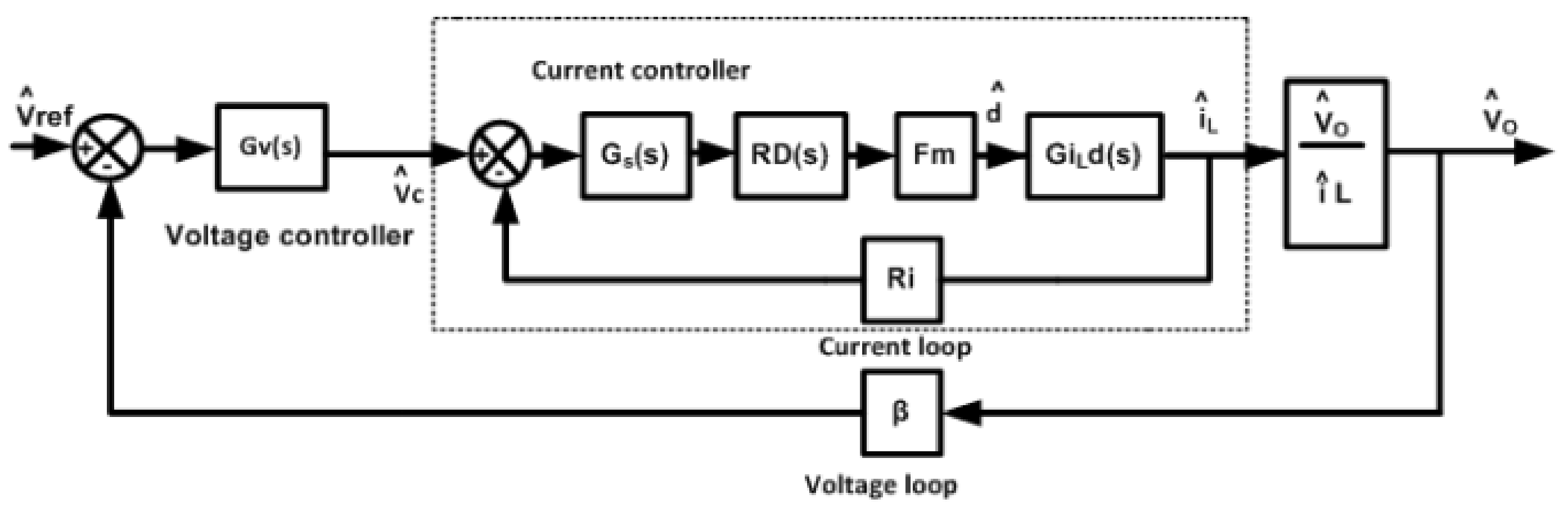
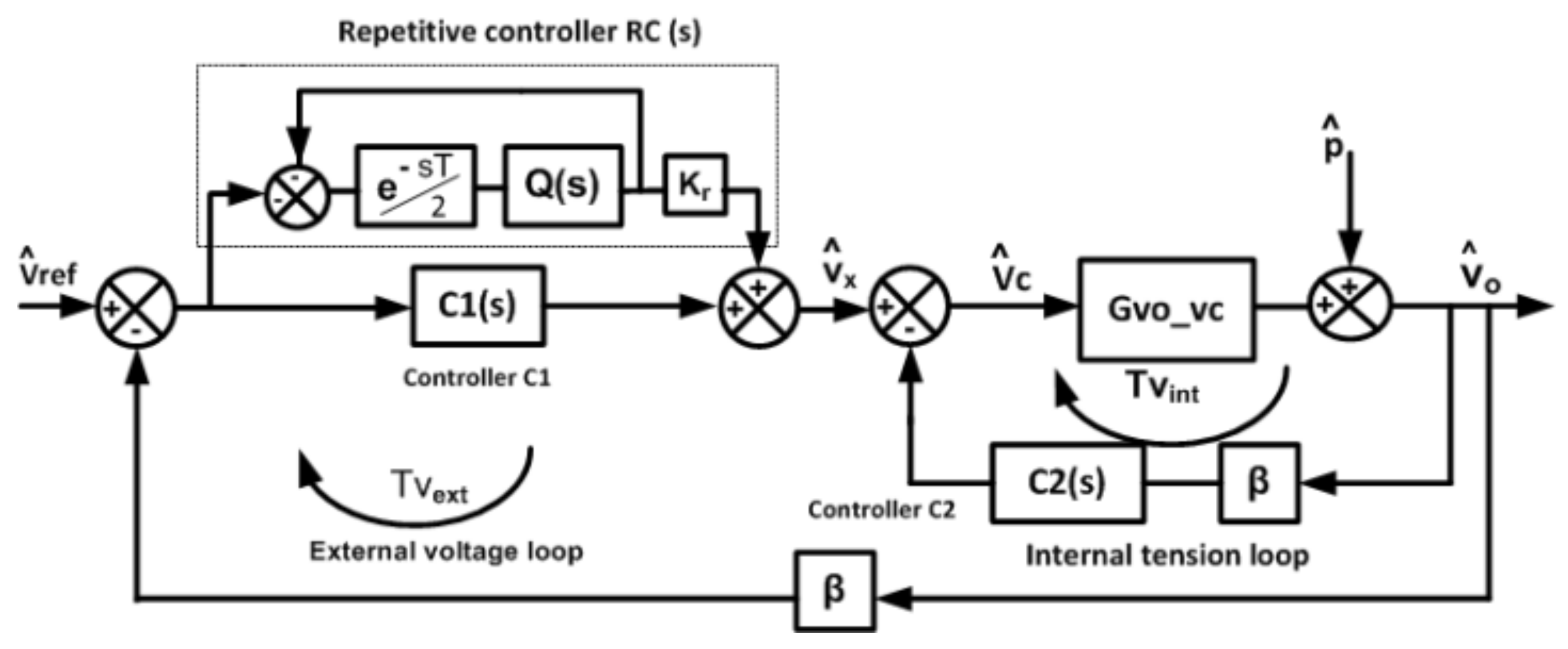
In this work, two control configurations are developed and applied: a two-degree-of-freedom control, plus a repetitive control (2DOF + RC) [22,23,24], and a proportional–integral–proportional control plus a resonant control (PI-P + ResC) and an integral–proportional control plus a resonant control (PI-P + ResC). The 2DOF controller guarantees the overall stability of the energy conversion system, allowing, at the same time, adequate setpoint tracking and disturbance rejection. This is achieved by the first controller implemented in the direct loop, and a second controller in the feedback loop, under different configurations derived from a proportional integral derivative controller (PID); for example, a PI controller in direct loop and a derivative controller in the feedback loop, obtaining a configuration (PI-D). The design of an integral controller in the direct loop and a derivative proportional control in the feedback loop is also possible, giving rise to a configuration (I-PD). In this work, we propose the design and implementation of a control structure with the following characteristics: a PI + RC controller, implemented in the direct loop, and a P controller implemented in the feedback loop. This configuration ensures that in the direct loop, the PI controller allows good setpoint tracking, and the addition of repetitive control contributes to the disturbances rejection, adding to this task the proportional controller implemented in the feedback loop. The implementation of this control configuration causes the inverter output closed-loop impedance to have a resistive characteristic at low frequencies and an inductive characteristic at high frequencies. Therefore, it is necessary to implement a resistive virtual impedance loop and choose a droop scheme with these characteristics to allow conversion units parallel connection.
Regarding the PI-P + ResC controller, it consists of two control configurations, a proportional integral–proportional controller (PI-P) plus a resonant controller (ResC). This configuration is structured by an integral proportional control in the direct loop plus a resonant controller, and a proportional controller in the feedback loop. As the control configuration described previously, the design of the PI-P controller assures the overall stability of the conversion system, while the resonant control is designed and implemented to improve the disturbances rejection, contributing to the task of the P controller implemented in the feedback loop. This configuration achieves good setpoint tracking and good disturbances rejection, in addition to the fact that a closed-loop impedance with resistive characteristics appears at the inverter output at high frequency. Thus, it is unnecessary to implement a virtual impedance loop and, therefore, we can choose a droop scheme with a resistive character for the inverters parallel connection.
Both configurations are a new proposal to solve the problem of reduction of total harmonic distortion and for inverter connection parallel, allowing a steady state error equal to zero (eee = 0), and the disturbance rejection with linear and non-linear load in the range between 1% and 2.5%, below the 5% required by the IEEE 519-1992 standard.
According to our simulations, good performance of the system is justified considering the following: with the implementation of these regulators, it is possible to have good setpoint tracking and good disturbance rejection, giving rise to a sinusoidal waveform of the voltage signal and maintaining the amplitude close to 230 V RMS, as well as its frequency. The reference voltage signal is obtained through droop schemes that allow the inverters connection in parallel to meet increases in load demand. For the present application, we chose a resistive droop scheme with a virtual impedance loop of the same characteristics that allows the inverters parallel connection and the homogeneous distribution of active and reactive power demanded by the load. The choice was determined considering that, with the implementation of both controllers, the inverter closed-loop impedance presents a resistive characteristic, which shows up in the Bode diagrams.
The present work is organized as follows: 
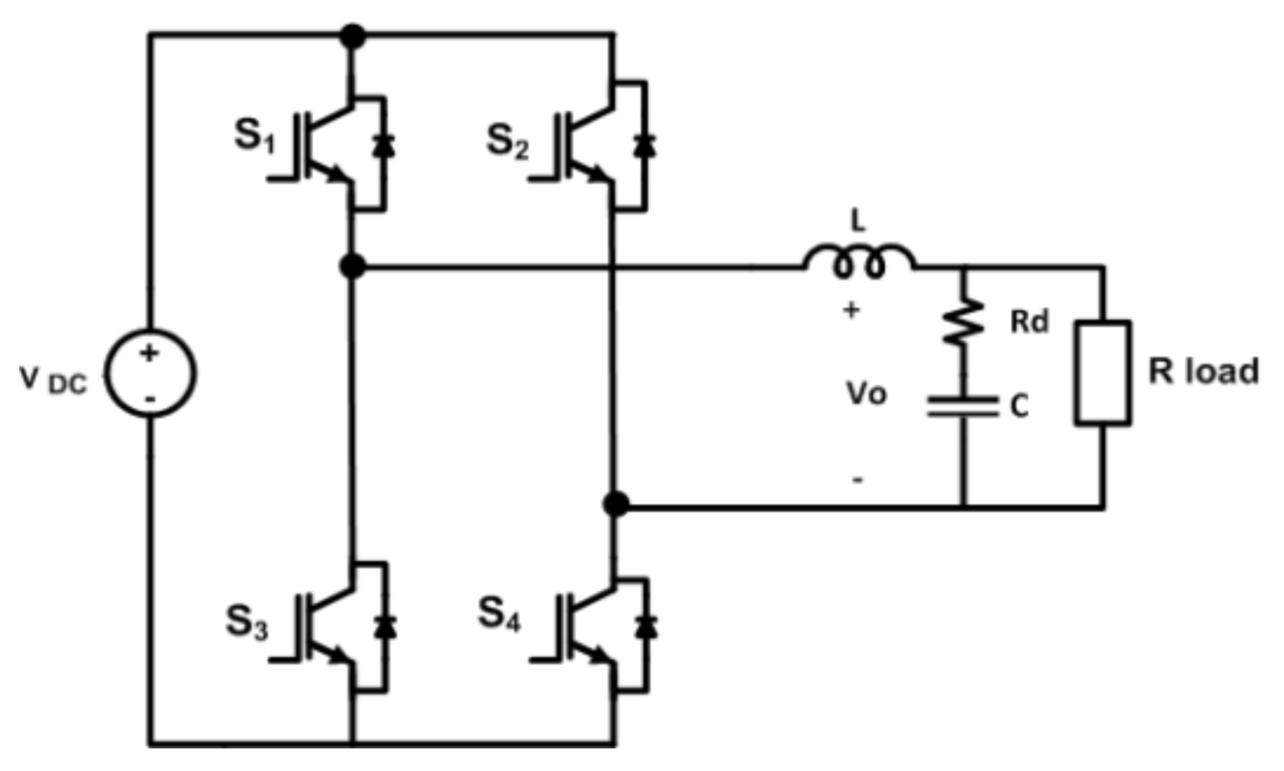
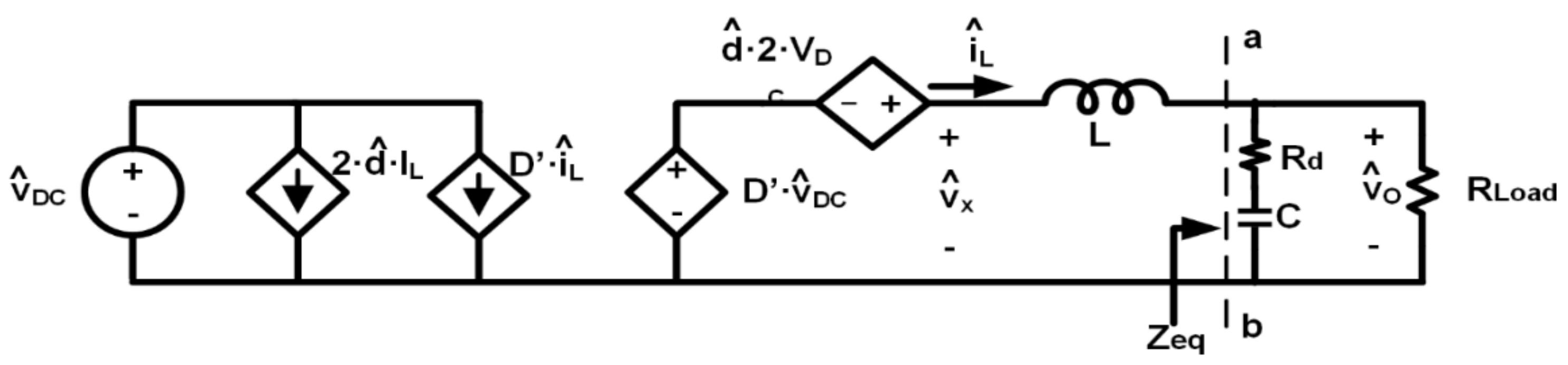
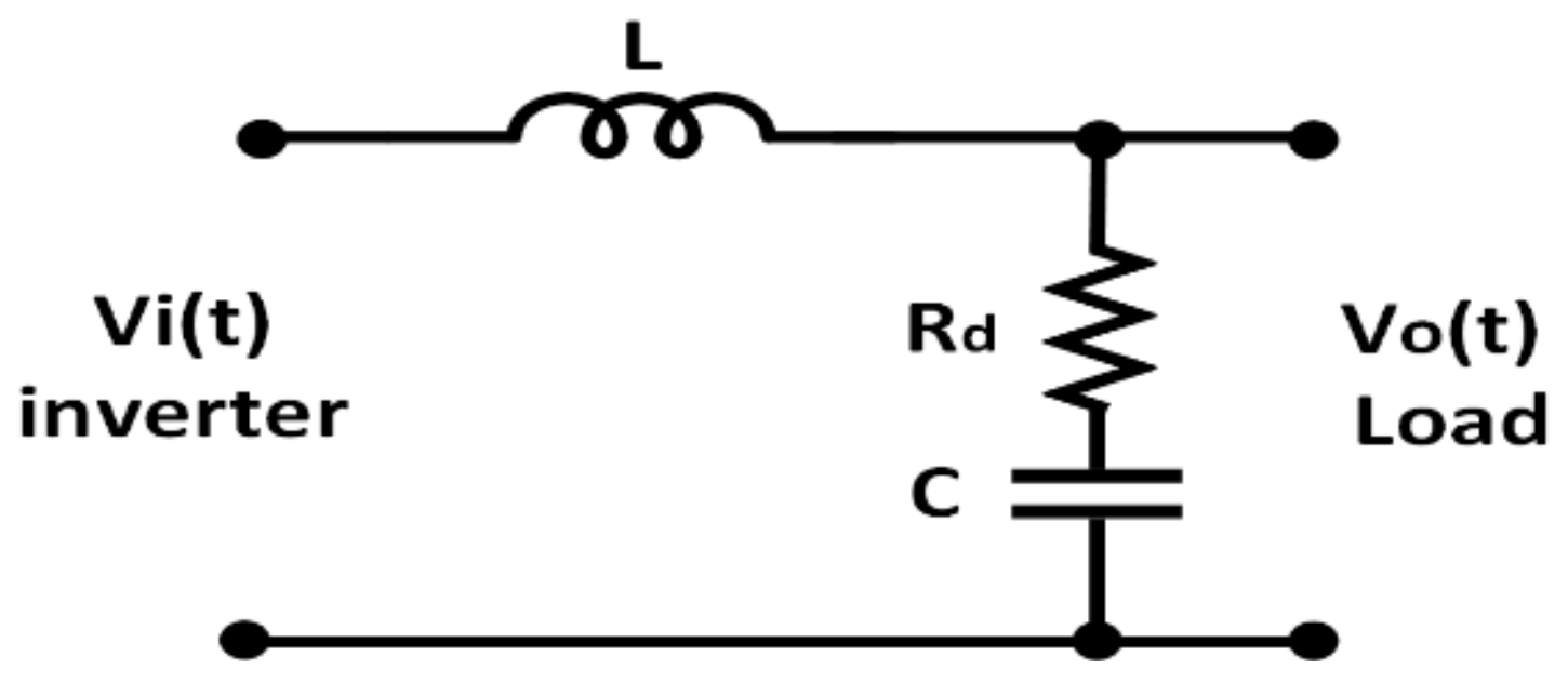
Section 2 describes the energy conversion system and the small signal model used to determine the transfer functions for the design of the current and voltage loops controllers. Section 3 describes the design of the controllers for the different control loops of the inverter. Section 4 presents the characteristics and design of the droop scheme used in the inverter. In Section 5, the analysis of the closed-loop impedance of the inverter with the controllers and the droop scheme employed is given. A description of the results of the simulations performed in PSIMTM [25] is provided in Section 6. In Section 7, the results obtained through experimental tests are presented. In Section 8, the discussion of the results obtained through simulations is presented. Finally, the conclusions are delivered in Section 9.

2. The Inverter System

An inverter schematic diagram implemented, an H-bridge type with bipolar Pulse-Width Modulation (PWM), whose nominal values are given in Table 1, is shown in Figure 1.

2.1. Small-Signal Model

To implement a feedback linear control from a non-linear circuit such as a power electronic converter, it is necessary to obtain a linear model [26]. To this purpose, it is necessary to identify the transfer functions corresponding to the control variables. The transfer functions are obtained using the commutated PWM model [27].
The small signal model is shown in Figure 2, with small perturbations around the operation point (OP). In this figure v ^ DC , i ^ L ,   d ^ y v ^ o , are small-signal terms and represent the inverter input voltage, the inductor current, the duty cycle, and the inverter output voltage, respectively. In addition, work cycle-to-the inductor current GiL_d(s) and the inductor current-to-voltage output Gvo_IL transfer functions, are obtained.

2.2. Inverter Output Filter Design

To obtain a sinusoidal output signal with the same voltage and frequency characteristics of the power grid, it is necessary to filter the VDC voltage present between output terminals the inverter single-phase full bridge. The topology used for the inverter is LC, as shown in Figure 3.
The LC filter has an attenuation of −40 db/decade above the resonant frequency and is generally used in situations where the load impedance around the capacitor is relatively higher for frequencies equal to and/or higher than the switching frequency.
Some characteristics that this filter must present when it is designed are: At the fundamental frequency, the capacitor must absorb little reactive power, so the current in the inverter connected inductor side is hardly increased by the capacitor; at the frequency of the switching harmonics, the capacitor must absorb the harmonics of the inductor current, which must be small.
Based on the above, we proceed to describe the calculation of the filter values that must meet the following conditions: The value of capacitor C is limited to the maximum consumption of reactive power allowed by the inverter.
For this case, if the maximum current in the capacitor is required to be less than 5% of the nominal current at full load, the magnitude is:
I c = 0.05 · I load
The capacitor impedance magnitude will be the output voltage divided by the current in the capacitor.
Z c = V o I c = V o 0.05   ·   S load V o = 2404.5   Ω
where Sload is the load nominal power and Ic the capacitor current.
Since the magnitude of capacitor impedance is, Z c = 1 / ω 1 C , the value of C is given by:
C = 1 ω 1 · Z c 1.3   μ F
where ω1 is the grid frequency expressed in rad/sec.
The inductor can be calculated in terms of its allowable voltage drop when the inverter output voltage is the nominal operating voltage.
If an inductor impedance (ZL) equal to or less than 10% of the load nominal impedance is required, then:
Z L 0.05 · Z load
The inductor impedance L magnitude is defined by Z L = ω 1 · L , solving for L gives:
L = Z L ω 1 = 0.1   ·   Z load ω 1 19.1   mH .
The LC filter resonant frequency must be between 10 times the grid frequency and half the switching frequency, to avoid resonance problems in the low and high part of the harmonic spectrum.
10 · ω 1 < ω res < ω s 2
where ωres is the LC filter resonant frequency, which is defined by (7) and ωs the switching frequency.
ω res = L + L g L · L g · C
To fulfill the conditions expressed in 1 and 6, a value of C = 600 nF is chosen, and it will be considered that the grid inductance Lg is ten times less than the inductor value inverter connected. One way to increase damping is by adding a resistor in series with the capacitor. It should be noted that selecting a very large resistance Rd will significantly reduce the oscillation at the resonance frequency and system efficiency. An additional criterion that can be included is based on placing a resistor that allows the attenuation of the inverter current control loop oscillation to be below 0 dB.

2.3. Control Scheme

Figure 4 shows the power inverter controls for the inductor current and the output voltage. In this figure, Gv(s) is the voltage controller transfer function, Gs(s) is the transfer current controller transfer function, and RD(s) represents a digital delay from a commutation period (Ts), given in Equation (8).
RD s = 1 s T s 2 + s T s 2 8 1 + s T s 2 + s T s 2 8 .
where Fm is the PWM modulator gain, defined in (9).
F m = 1 V pp Triangular = 1
In Figure 3, Ri = 0.2 and β = 0.006, are the current and voltage sensor gain, respectively.
The main advantage, of this control scheme, is that the transfer function response is flatter than the reference voltage and less distorted than the peak-current control (PCC). For the current-loop design, it is important the function that relates the output-current and the work-cycle, given by:
G iL _ d s = i ^ L d ^ v ^ DC = 0 = 2 · V DC Z a + s · L ,
where VDC is the voltage in the DC_Link, and Za is the load impedance in parallel with the damping resistance and the output capacitor:
Z a = R d + 1 sC R =   s · C · R d + 1 · R s · C R d + R + 1 ,

3. Controller Design

3.1. Current Controller Design

The current controller implementation starts with a resonant controller (ResC), or a harmonic controller if its frequencies are multiples of the fundamental [28], and a proportional control (P). Such a controller has the objective of providing in a high gain to the reference signal frequency in the current loop to inhibit the effect of any grid disturbances present. A decision was made to implement a single resonant to the grid frequency. This is justifiable, since the objective of the islanded inverter is to keep the wave-shape, amplitude, and voltage signal frequency delivered to the load, not to the current signal.
In the inverter design, it is advisable to have a crossing frequency in the current loop, ten times smaller than 20 kHz, the inverter commutation frequency, which is about 5 dB gain factor and phase larger than 50 degrees, keeping appropriate stability margins [29]. For the present application, a P + Resonant (P + ResC) controller was chosen, defined by Equation (12).
G S s = K P + K h B h s s 2 + B h s + ω h 2 ,
where:
  • ω h = h ω O where h is a resonance with a frequency multiple of the fundamental;
  • Kh = the peak resonance gain at the frequency ωh;
  • Bh = the bandwidth, where the resonance has a gain.
For this application, the following resonant parameter values were established: h = 1 ,   k h = 100 ,   B h = 2 · π ,   ω 0 = 2 · π · 50 , and:
K P = L ω c _ desired R i F m 2 V DC = 1.34 ,
with ωc desired = 2 π 1800.
The resonant control parameters, such as the gain at the resonance peak Kh and its bandwidth Bh, are determined so that its input in the current loop has no effect in the system global stability, keeping appropriate values for stability parameters like phase, gain margins, and cross frequency. As for ωc_desired, this value is chosen to be close to half of the inverters commuting frequency.
The current control loop scheme (Figure 4) is shown in Figure 5. It has a PM: 64.5°, GM: 8.5 dB, and BW: 2.21 kHz, and it is defined by Ti(s) = GiL_d(s)·Fm·Ri·Gs(s).

3.2. Voltage Controller Design

The voltage controller design is done with the average current control (ACC) scheme. This controller regulates the inverter output v ^ o and provides a fixed reference for the current controller. The transfer functions of interest for the voltage-loop controller design relate the output voltage with the work cycle, Gvo_d(s), and the output voltage with v ^ c , Gvo_vc(s), as determined by Equations (14)–(16):
Gv o _ d s = v ^ o d ^ i ^ DC = i ^ o = 0 = 2 · V DC · Z a Z a + s · L ,
G vo v c s =   v ^ o i L · i ^ L v ^ C = v ^ o d ^ · i ^ L d ^ 1 · i ^ L v ^ C = v ^ o v ^ C ,
where:
G iL Vc s = i ^ L v ^ c = T i s R i · 1 + T i s ,
The design incorporates the following control configurations: proportional integral-proportional plus resonant (PI-P + ResC) and two degrees of freedom plus repetitive controller (2DOF + RC). These controllers aim at getting good reference tracking and reducing the harmonic distortion of the output voltage when the inverter feeds linear and nonlinear loads. Considering that the voltage-loop controller sets the reference for the current-loop controller, the former must be designed with a smaller bandwidth.

3.2.1. 2DOF + RC Design

The 2DOF + RC control configuration is made up of two controllers, a two-degree-of-freedom controller (2DOF) plus a repetitive controller (RC). Particularly, the 2DOF controller is initially implemented so that its design guarantees the overall stability of the energy conversion system, allowing at the same time an adequate setpoint tracking and better perturbances rejection. This is achieved by implementing a controller in the direct loop whose objective is to provide an adequate setpoint tracking, the other controller is implemented in the feedback loop and its objective is to improve the disturbances rejection. Particularly, in this work a PI + RC control is implemented in the direct loop and a P controller in the feedback loop. It is highlighted that the repetitive controller that is located in the direct loop, is added to the disturbance rejection task that the controller P attends designed for the feedback loop; which increases the robustness of this control configuration. This control configuration presents at low frequency a closed loop impedance with resistive characteristics, however, at higher frequencies it presents an inductive characteristic. These characteristics make it necessary to implement a resistive virtual impedance loop and choose a droop scheme with these characteristics, to allow parallel connection of inverters.
The design of the 2DOF + RC controller is based on the scheme of Figure 6 and is subdivided into two stages. In the first stage, the control scheme of two degrees of freedom is designed and finally, in order to improve the level of rejection to disturbances, the RC controller is added. Figure 6 shows the detail of the voltage loop; the current loop is presented as a closed-loop transfer function Gvo_vc. The RC(s) block represents the repetitive controller and C1(s) and C2(s), represent classical controllers.
The 2DOF control configuration aims at designing the C1(s) controller to perform an accurate tracking of the OP, and the C2(s) controller to carry on an appropriate level of disturbance rejection; that is, implementing both controllers imply that Equations (17) and (18) are fulfilled, and that the response in both situations quickly dampens, with zero error in steady state.
G vo _ vref = v ^ o v ^ ref 1 β   ,
G vo _ p = v ^ o s p ^ s 0 ,
The design of these controllers must meet the condition in Equation (19) [13].
lim s 0   C 2 s C 1 S = 0 ,
For designing purposes, a PI controller action is recommended for the C1(s) controller, and a proportional action for the C2(s) controller. These controllers will have the objective of providing the system with an adequate tracking setpoint and disturbance rejection, respectively.
The C1(s) and C2(s) controllers design begins with the closed-loop transfer function that relates the response of the system to the perturbation input in Equation (20). Considering that this response involves both controllers, a simplifying design step is taken by considering Equation (21).
G vo _ p = v ^ o s p ^ s = 1 1 +   C 1 s + C 2 s Gvo _ vc s β ,
where:
C s = C 1 s + C 2 s .
Then:
G vo _ p = v ^ o s p ^ s = 1 1 +   C s Gvo _ vc s β
The designing steps are:
Step 1.
Initially, C(s) is designed for the system to show an appropriate response v ^ o to an input disturbances signal p ^ , assuming that the input reference is zero.
Given the dynamical features of the power plant under discussion, a PI(s) controller with the structure shown in (23) is proposed as a first approach to the expected solution. This controller is designed with adequate disturbance rejection levels and appropriate stability parameters. Its design is recommended for a frequency two times smaller than the crossing frequency of the current loop.
C s = PI s = K · s + a / s .
Step 2.
The C1(s) controller design has the main objective of providing the system with an adequate tracking setpoint, assuming that the perturbation input is zero. This design is based on Equation (24) that relates the system response v ^ o with the reference input v ^ ref .
G vo _ vref = v ^ o v ^ ref = Gvo _ vc C 1 s 1 + C 1 s + C 2 s Gvo _ vc s β
In turn, Equation (24) may be rewritten as (25).
G vo _ vref = v ^ o v ^ ref = Gvo _ vc C 1 s 1 + C s Gvo _ vc s β
Once the C(s) and C1(s) controllers have been designed, we design C2(s). Solving C2(s) from Equation (21), the design features of the C2(s) controller get determined from Equation (26).
C 2 s = C s C 1 s ,
Following this strategy and checking that the conditions imposed by Equations (17)–(19) are met, the controllers C1(s) and C2(s) are designed. In the event that they are not met, we return to Step 1, and a new controller C(s) is proposed. This new scheme must contain an integral part that guarantees the disturbances rejection. A proposal for this second iteration can be of the form.
C s = k s + a s + b s s + c ,
Considering the above conditions, the C1(s) and C2(s) controllers have the following values:
C 1 s = 0.10988 s + 5700 s ,
C 2 s = 3144 1 s + 8200 ,
On the other hand, in order to improve the level of rejection of disturbances, ensuring that the global stability of the system is not affected, it is proposed to design a repetitive RC(s) controller. Its design is based on Equations (30) and (31).
RC s = Q s · e sT 1 Q s · e sT Kr ,
Q s = 1 s 2 ω q 2 + 2 ε ω q s + 1 .
where:
  • Q(s) = represents a low-pass filter of infinite response, to second order pulse;
  • e sT = represents a delay;
  • T = 0.02   s ;
  • ω q = 2     π     f q   rad / seg (cut frequency);
  • ε = 0.707 (damping factor);
  • f q = 400 Hz;
  • Kr = 0.5 (repetitive controller gain).
The fq and Kr terms are chosen to provide adequate stability levels.
Applying block algebra to Figure 6, the gain in the voltage-loop 2DOF plus Repetitive Controller (2DOF + RC) is expressed by (32):
Tv s = C 1 s + RC s + C 2 s · G vo _ vc · β ,
On the other hand, the voltage loop gain considering a PI plus RC controller is:
Tv s = C 1 s + RC s · G vo _ vc · β
In Figure 7, voltage loop open-loop gain Bode diagram with 2DOF + RC control and with PI + RC controller is shown, observing that for similar Nyquist stability design criteria ((crossover frequency) fc = 978 Hz, (phase margin) PM = 92.5°, (Gain margin) GM = 6.2 dB); the 2DOF + RC controller has a higher gain at the load harmonics frequency, which guarantees a higher disturbances rejection. This behavior is observed in the blue graph, where it is justified that for the fundamental frequency (50 hz), 3rd, 5th, 7th, and 9th load harmonic, the gains that are presented are higher; another important aspect is that the resulting phase with the 2DOF + RC controller design presents a resistive characteristic close to 0°, which contrasts with the PI + RC controller phase, which at frequencies close to 1 kHz presents an inductive character, which results in to present a lower disturbances.

3.2.2. PI-P + ResC

The PI-P + ResC control configuration consists of a proportional–integral–proportional (PI-P) controller plus a resonant controller. This configuration contains an integral proportional control in the direct loop, plus a resonant controller and a proportional controller in the feedback loop. As in the previous control configuration, the PI-P controller is designed to warrant the overall stability of the conversion system and the resonant control is designed and implemented to improve upon the disturbances rejection, helping in the task performed by the P controller, implemented in the feedback loop. Particularly, this control configuration presents a closed-loop impedance with resistive characteristics at the inverter output, in a wider frequency range than with the previous controller; thus, it is not necessary to implement a virtual impedance loop and a resistive droop scheme can be chosen directly.
A schematic of the PI-P + resonant controller is shown in Figure 8. The purpose of this controller is to provide the system with adequate disturbance rejection for linear and non-linear loads, while keeping accurate tracking and considering that the energy conversion units should be parallel connected to take care of load surges. The detail of this design is published elsewhere [30].
The basic idea of PI-P control is to prevent large control signals that can cause saturation phenomena within the system. Adding the resonant driver improves the disturbances rejection due to the presence of non-linear loads, keep good track of the set point.
Controller C2(s) was adjusted to have adequate rejection of disturbances following the recommendation that its bandwidth be less than that of the current loop.
C 2 s = 0.3 ,
On the other hand, the controller C1 aims to present good setpoint tracking with status error null stationary. For this application, the controller that meets this characteristic is as follows.
C 1 s = 0.080266   · s + 11600 s ,
The next step is to design the resonant controller. As shown in Figure 8, this is in parallel with the control C1 (s). This controller is designed so that its insertion does not affect the overall stability of the system and its objective is to contribute to the disturbances rejection and to provide a high gain in harmonic frequencies produced by the load.
The resonant controller design parameters of Equation (36) are given in Table 2.
ResC   =   h = 1 11 K h B h s s 2 + B h s + ω h 2 ,
The voltage-loop gain Tv(s) for PI-P + ResC is given by:
T V s ext = C 1 s + ResC G int s β ,
On the other hand, the voltage loop gain considering a PI plus ResC controller is.
T V s ext = C 1 s + ResC β
Figure 9 shows voltage loop open-loop gain Bode diagram of PI-P + ResC control and the of PI + ResC controller, observing that with equal Nyquist stability design criteria: (phase margin 58.2°, gain margin 7.6 dB and bandwidth of 980 Hz); in the PI-P + ResC control configuration; more resonant can be designed. Particularly, resonant are implemented at the signal fundamental frequency and the load harmonics: 3rd, 5th, 7th, 9th, and 11th. This contrasts with the resonant number that can be implemented with the PI + RC control configuration; that is, for the same crossover frequency, only resonant at voltage signal fundamental frequency and load frequency harmonics could be implemented: 3rd, 5th, and 7th. An important aspect is that both configurations have a resistive phase with a phase close to 0°. This finally allows that the configuration PI-P + ResC presents a greater disturbances rejection.

4. Droop Schemes

This scheme has two advantages, the first one being the setting of a dynamic voltage reference responsive to the active and reactive power of the load demand. This is based on the possibility of connecting several inverters in parallel, without the need of using concentrated control or master–slave control. The second advantage is that it is not necessary to send control signals throughout different communication channels [31]. The behavior of the droop scheme is represented by Equations (39) and (40).
f f 0 = k p Pa P 0 ,
U U 0 = k q Q Q 0 ,
where:
  • f0 = frequency nominal;
  • U0 = nominal voltage;
  • P0 = active power of the inverter at the reference point;
  • Q0 = reactive power of the inverter at the reference point.
The frequency and voltage features of the droop control are functions of the active and reactive power demanded by the load. Equations (35) and (36) show that adjusting active power Pa and reactive power Q modify voltage amplitude and frequency, respectively.

5. Impedances

5.1. Inverters Output Impedance

The power distribution amongst converters units is directly affected by the inverter output impedance closed-circuit and defines the droop control strategy to use in the inverter parallel connection units. In addition, an adequate design of output impedance may reduce the impact of unbalance in the line impedance. When Zolc is only inductive (Zolc = jX), the phase is 90° and 0° when Zolc is only resistive.
For this application, a droop scheme with resistive characteristics was chosen, considering that the calculations of the inverter closed-loop output-impedance pointed towards such feature. That is, with the inverter current and voltage loop controller implementation [32].

5.2. Virtual Impedance Loop

The traditional droop method is inadequate if the inverters parallel connected share non-linear loads, since the control units must consider the harmonics of the current signal, while balancing the active and reactive power [33,34,35]. Under this assumption, novel and fast control loops have been proposed, called virtual impedance loops. These controllers adjust the inverter output impedance closed-circuit to warrant their impedances to be resistive [36] or, sometimes, inductive [37]. Figure 10 exhibits a block-diagram that shows the inverters control-loops, including the virtual impedance loop.
To be able to estimate the inverters closed-loop/open-loop output impedance ( Z O _ LC (s) and Z O _ LA s , respectively), it is necessary to start from the small signal analysis, as shown in Figure 10.
The transfer function Z O _ LA s is obtained making v ^ DC = v ^ C = 0 ; i.e., assuming that there are no voltage variations in the DC_Link. Za(s) in Equation (41) is the impedance connected to the right of the inverters output-filter inductor.
Z a s = R · s · C · R d + 1 s · C · R d + R + 1 ,
Applying Kirchhoff’s laws to the small-signal model in Figure 10, considering that v ^ DC = 0 , Equation (42) is obtained:
Z O _ LA = v ^ o i ^ o ,
where i ^ o represents the current perturbation at the inverter’s output. When the voltage loop is open ( v ^ C = 0 ) and Equation (43), may be obtained from Figure 9.
d ^ = K s · i ^ L ,
where, K s = Fm · Ri · Gs s · RD s .
v ^ o = i ^ L i ^ o · Z a ,
Considering:
2 V DC · K s · i ^ L = s · L · i ^ L + v ^ o ,
Solving i ^ L from (45):
i ^ L = v ^ o 2 V DC · K s s · L ,
Substituting (46) in (44), gives:
v ^ o = v ^ o 2 V DC · K s s · L i ^ o · Z a ,
From Equation (48), the following expression results:
v ^ o · 1 Z a 2 V DC · K s s · L = i ^ o · Z a ,
Finally, from Equation (49) the open-loop inverter’s output impedance is given by:
Z O LA s = v ^ o i ^ o v ^ C = 0 = Z a 2 V dc · K s s · L 2 V dc · K s s · L Z a ,
The inverter output impedance closed loop is given in Equation (50), where Tv(s) represents the different gains in the voltage loops obtained by applying the controllers used for this purpose.
Z O _ LC s = v ^ o i ^ o V ^ DC = v ^ Ref = 0 = Z o LA s 1 + T V s ,
From Figure 10, it is possible to determine the virtual impedance loop that is obtained with (51).
Z O _ LC _ Z V s = Z O _ LC s + Z V s G vo _ vref s ,
where
G vo _ vref s = 1 β · T V s 1 + T V s ,
The value of ZV(s) must be larger than Z O _ LC s and the maximum line impedance expected. For the present application, the value assigned to the virtual impedance was ZV(s) = R = 0.2.
Applying Equations (42) and (43), and using Bode diagrams, the inverter’s closed-loop output impedance characteristic is obtained, with or without virtual impedance, for each of the controllers implemented in the voltage loop and the controller in the current loop.
Figure 11 evinces the effect of the two implemented controllers. The P + ResC controller, implemented in the current loops, and 2DOF + RC controller, implemented in the voltage loops; without implementing the virtual impedance loop, at low frequency, the inverter’s closed-loop output impedance exhibits a resistive characteristic, i.e., the phase angle is almost zero up to the fourth harmonic and then increases. In contrast, when the virtual impedance is implemented, a resistive characteristic extends over a larger range of frequency and harmonics may appear due to the load. This feature of the impedance produces less distortion to the inverter’s output voltage when feeding non-linear loads, forcing a resistive droop scheme for the converters in-parallel connection. Simulations performed in PSIMTM support these results.
Figure 12 shows the effect of the P + ResC controller, implemented in the current loops, and PI-P + ResC controller, implemented in the voltage loops. The inverter’s closed-loop output impedance is practically constant, for the fundamental frequency and harmonics of the load’s current, implying a resistive behavior with phase close to 0°. It is highlighted that the observed behavior for the inverter’s closed-loop output impedance occurred without implementing a virtual impedance loop. For this reason, the in-parallel connection loop was omitted. The simulations performed in PSIMTM justify this procedure.

6. Simulation Result

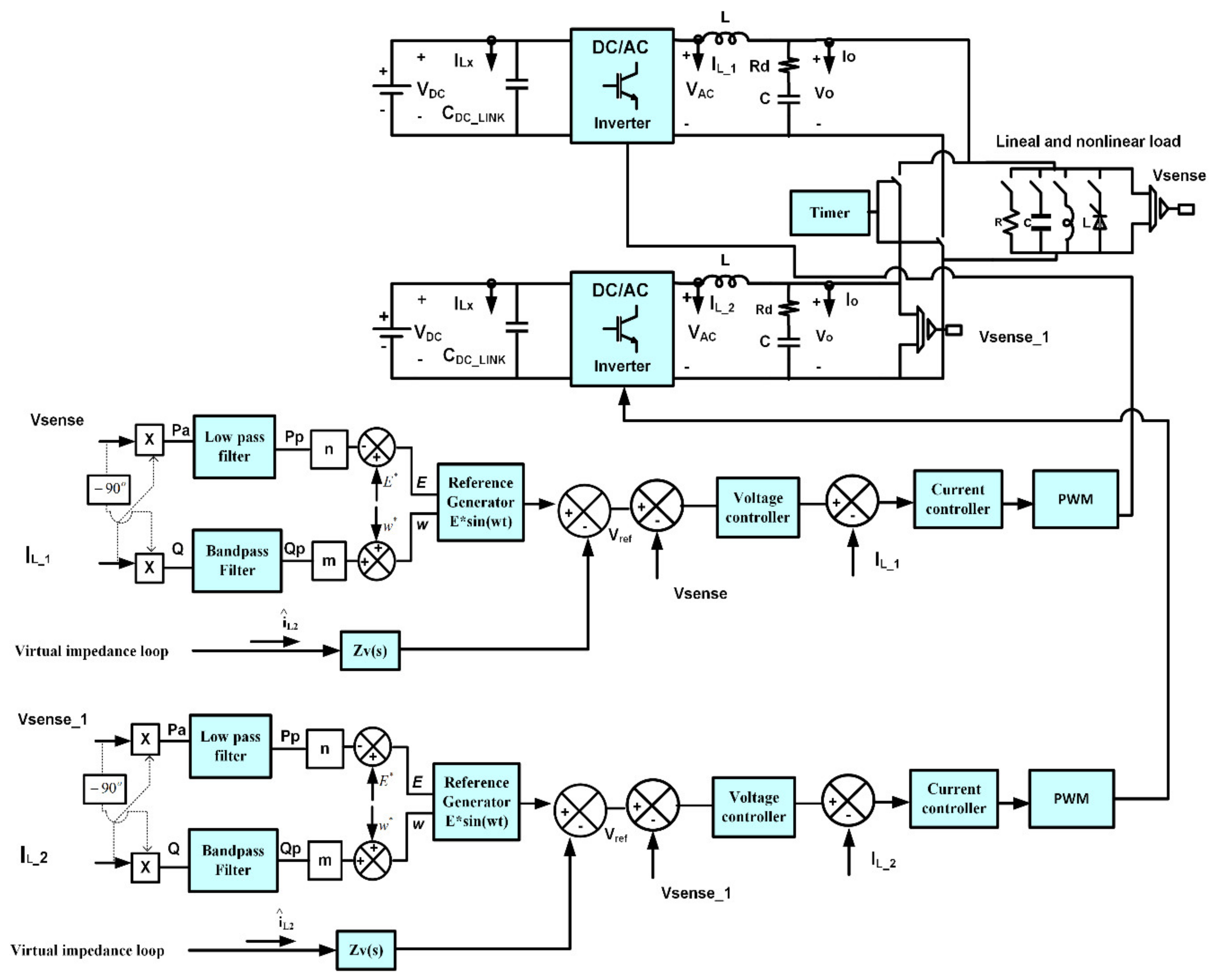
The simulations were carried on by implementing the diagram in Figure 13, in the PSIMTM simulator, showing the schematic of two inverters connected in parallel, with a droop scheme and resistive virtual impedance loop.
The testing was performed using a resistive linear load of 170 Ω, and with a non-linear load consisting of a mono-phasic full-wave rectifying bridge, interconnected with a 96 μF capacitor and a 680 Ω resistance. This load presents a crest factor CF = 4.6.
Figure 14 shows the waveforms of the output voltage and current signals of the inverter island mode operation with the implementation of the P + ResC controller in its current loop and the PI + ResC controller in its voltage loop; the simulation is done by feeding the non-linear load mentioned above. In this figure, the voltage signal presents a distortion of 4.6%, which is justified since its waveform in the maximum and minimum peaks is not sinusoidal, presenting an amplitude of 225 V RMS value that is less than the expected one that corresponds to 230 V RMS. Additionally, the current signal has a characteristics waveform of the non-linear load. The total harmonic distortion is below the 5% recommended according to IEEE 519-1992.
Figure 15 shows the waveforms of the output voltage and current signals of the inverter island mode operating with the implementation of the P + ResC controller in its current loop and the PI-P + ResC controller in its current loop and tension; the simulation is done by feeding the non-linear load mentioned above. In this figure, the voltage signal presents a distortion of 2.5%, which is justified since its waveform in the maximum and minimum peaks presents a more sinusoidal behavior compared to that obtained with the controller application previously presenting; being its amplitude of 229 V RMS; A value that is higher than that obtained with the previous controller implementation and is very close to the one expected, 230 V RMS. Additionally, the current presents a waveform typical of the non-linear load, being evident that the total harmonic distortion is well below the 5% that is recommended according to the IEEE 519-1992 standard.
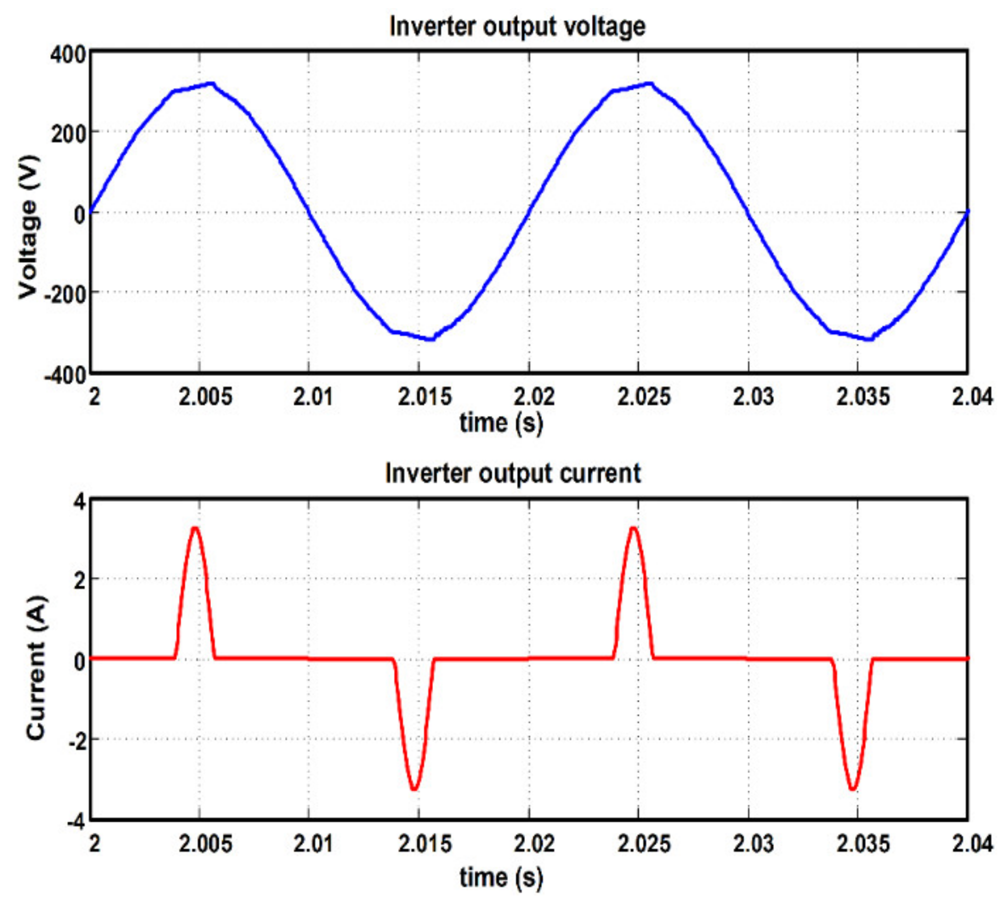
Figure 16 shows the waveforms of the output voltage and current signals of the inverter island mode operation with the implementation of the P + ResC controller in its current loop and the PI + RC controller in its voltage loop; the simulation is done by feeding the non-linear load mentioned above. In this figure, the voltage signal presents a distortion of 4.8%, which is justified since its waveform in the maximum and minimum peaks is not sinusoidal, presenting an amplitude of 226 V RMS value that is less than the expected one that corresponds to 230 V RMS. Additionally, the current signal has a characteristics waveform of the non-linear load. The total harmonic distortion is below the 5% recommended according to IEEE 519-1992.
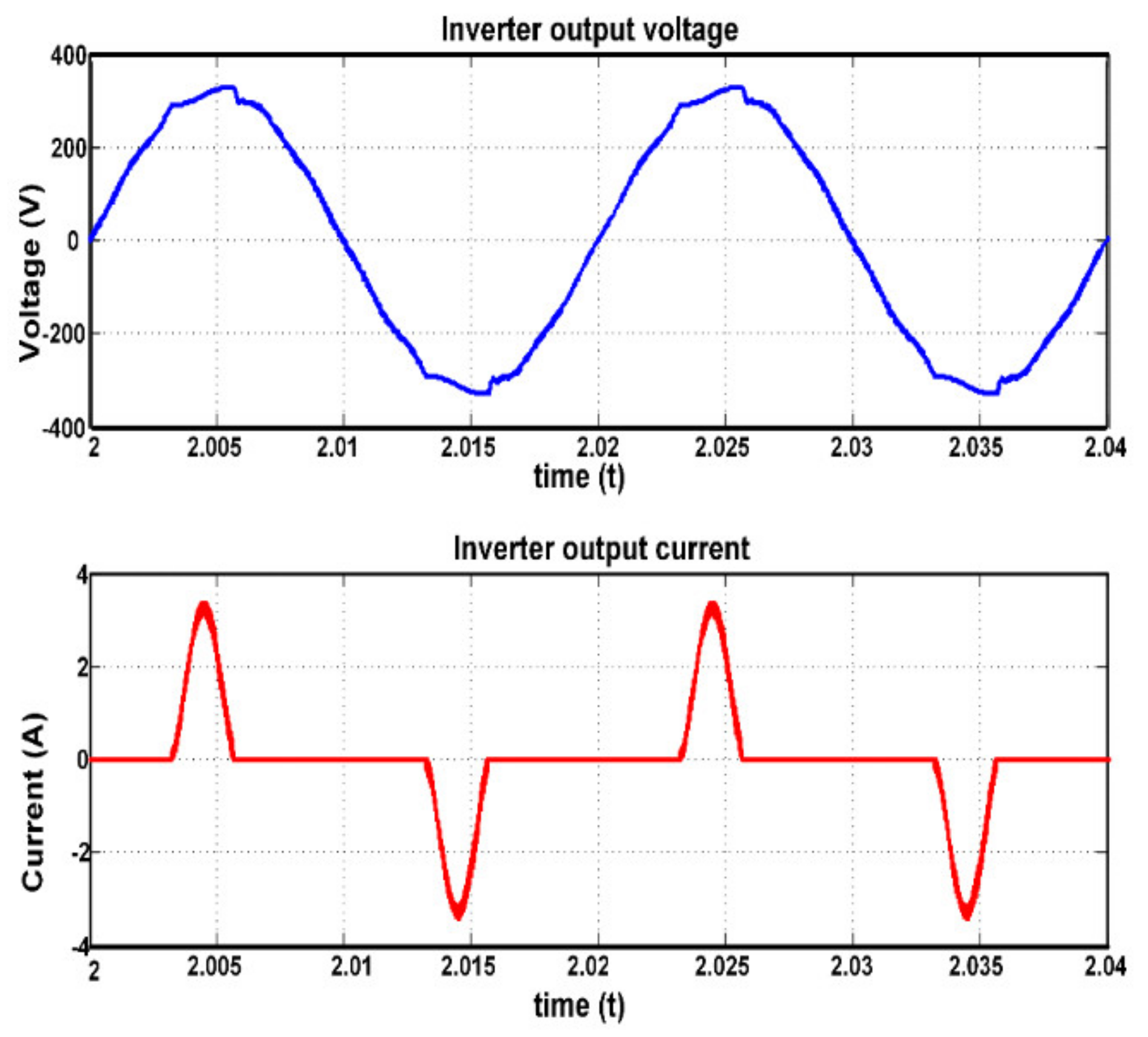
Figure 17 shows the waveforms of the output voltage and current signals of the inverter island mode operating with the implementation of the P + ResC controller in its current loop and the 2DOF + RC controller in its current loop and tension; the simulation is done by feeding the non-linear load mentioned above. In this figure, the voltage signal presents a distortion of 2.5%, which is justified since its waveform in the maximum and minimum peaks presents a more sinusoidal behavior compared to that obtained with the controllers application introduced earlier (PI + ResC, PI-P + ResC and PI + RC), obtaining with the 2DOF + RC controller an amplitude in the voltage signal of 230 V RMS, a value that is greater than that obtained with the controllers implementation previous, this being the expected value. Additionally, the current presents a waveform that corresponds to the non-linear load, being evident that the total harmonic distortion is well below the 5% that is recommended according to the IEEE 519-1992 standard.
Figure 18 shows the wave shapes of voltage, current, active, and reactive power obtained with the in-parallel connection of two inverters feeding a nominal purely resistive load. The simulation was carried on with the P + ResC controller implemented in the current loop and 2DOF + RC controller implemented in the voltage loop, and a resistive virtual impedance loop. Both inverters share the load and active power, with a suitable transient response at the time of their interconnection. These results are equivalent to those obtained by applying the PI-P + ResC controllers and, therefore, are omitted.
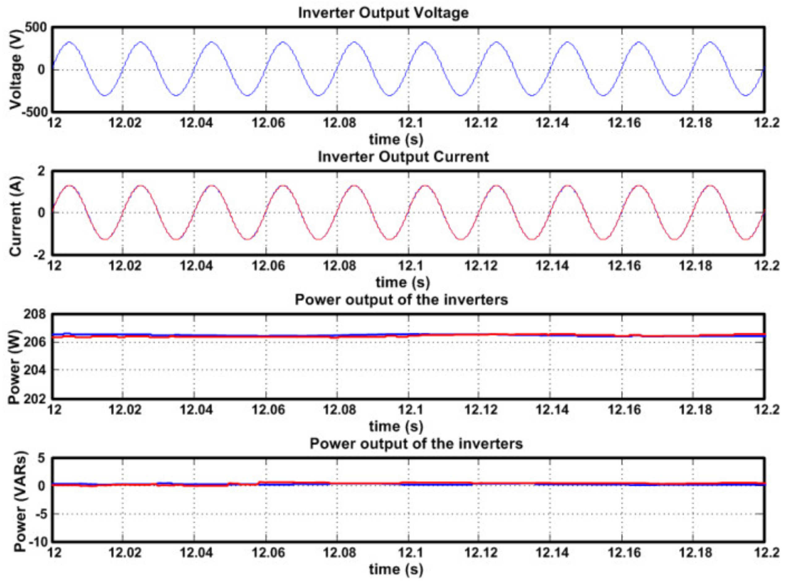
Figure 19 shows a zoom-in in the time scale (12 to 12.2) of the wave shapes of the voltage, current, and power in Figure 18. The wave shape of the inverters’ output voltage is kept, with an adequate balance of load and reactive power between them. These results are equivalent to those obtained by applying the PI-P + ResC controller. The simulations performed are left out.
Figure 20 shows the wave shapes of current, voltage and active power, of two inverters feeding a non-linear load. The load has a nominal value equal to one third of the total inverter’s power. This simulation was carried on with the P + ResC controller implemented in the current loop, and 2DOF + RC controller, implemented in the voltage loops and a resistive virtual impedance loop. In the simulation, an appropriate transitory response at the interconnection was observed, a balanced share of load and active power between both inverters.
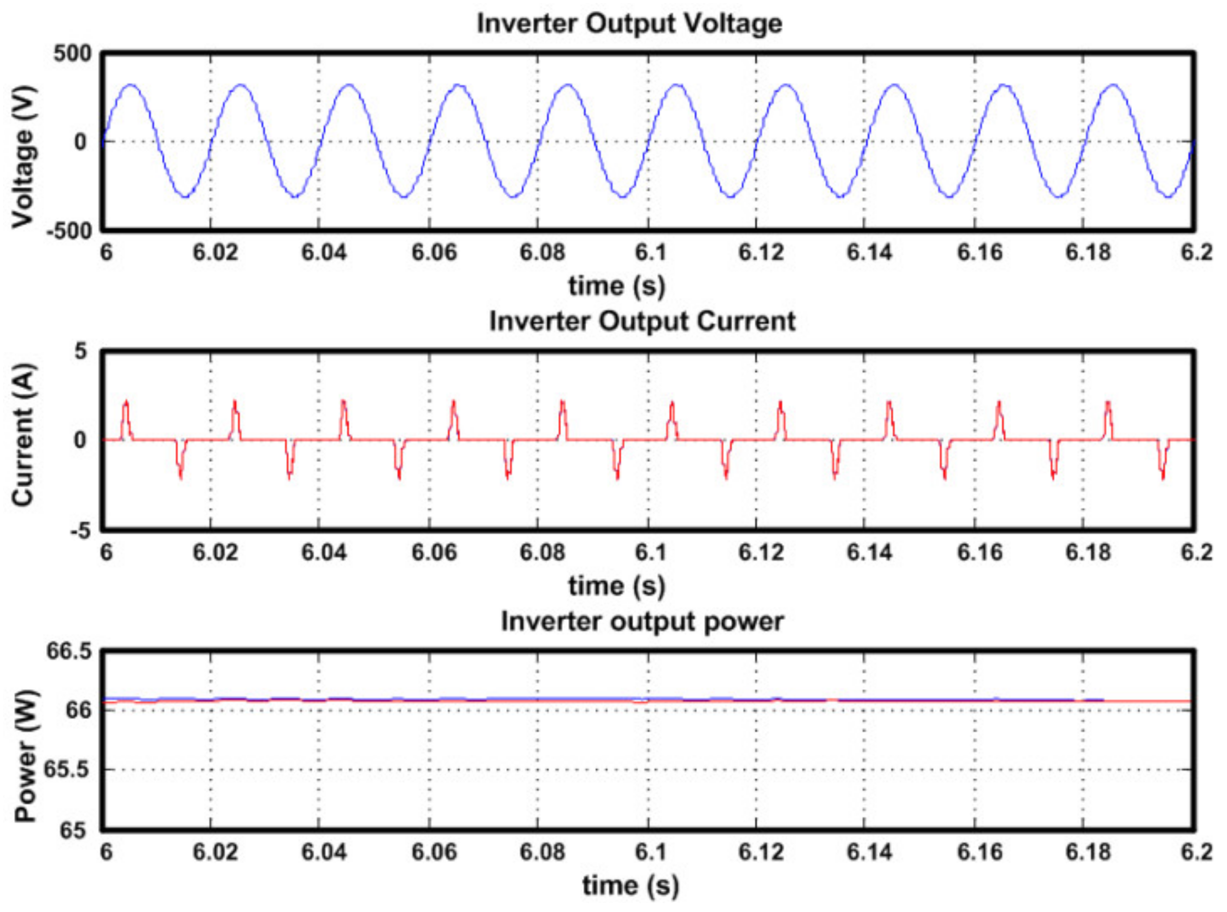
Figure 21 shows a zoom-in of Figure 20 in the time scale (6 to 6.2) of the wave shapes of the voltage, current, and output power. In Figure 21, the output voltage signal shows a small distortion. However, the proposed control still provides a better wave shape in the output voltage of the inverters than the previously introduced controllers. Like before, the load and active power shares appear adequately balanced between both inverters.
Figure 22 shows the waveforms obtained from the simulation of the P + ResC and PI-P + ResC controllers, with an in-parallel configuration of two inverters feeding a non-linear load equivalent to one third of the inverter’s total nominal power, without implementing a virtual impedance loop. It is possible to observe a balanced share of load and active power between inverters and an appropriate transient response when interconnected.
Figure 23 shows a zoom-in of Figure 22 in the time scale (6 to 6.2) of the wave shapes of the voltage, current, and output power. The obtained signal is quite similar to the 2DOF + RC controller, because the output voltage signal also shows a small distortion. According to Figure 15 and Figure 17, which means that implementing either the 2DOF + RC or the PI-P + ResC controllers in the voltage loop, produces an appropriate voltage wave-shape at the inverters’ output, with load and active and reactive powers balanced between both inverters.

7. Experimental Results

Inverter experimental tests performance feeding a non-linear load are reported, with the 2DOF + RC and PI-P + ResC controller implementation, as well as a parallel connection test of two inverters.
Experimental measurements have been carried out on the 440 W inverter described in Section 2. The controllers were implemented on a TMS320F28335 processor with a sampling frequency of 40 kHz. The sampling frequency is justified by applying the sampling theorem. The results obtained through simulations are like those obtained using experimental tests, so its presentation was not considered in this work.
The tests were performed with a resistive linear load of 170 Ω, and with a nonlinear load composed by a single-phase diode rectifier with a filter capacitance of Cf = 90 μF and a resistance of 680 Ω. It is worth pointing out that the rectifier has no input inductance, so that a highly nonlinear load results with a crest factor of CF = 4.2 and S = 130 VA when connected to an ideal sinusoidal mains voltage of 230 VRMS.
Figure 24, shows the experimental response of the output voltage and output current when the inverter powers the non-linear load using the 2DOF + RC controller. This graph shows a voltage signal with a total harmonic distortion THDv = 2.2%, a value that is below the 5% recommended by the IEEE 519-1992 standard. It is important to mention that the crest factor (CF) of this load corresponds to a value of 4.2, value that is considered high for a non-linear load. An important aspect is that the voltage signal has an amplitude of 228.5 V RMS, when the expected nominal value according to the converter operating power is 230 V RMS; which justifies the good performance of the controller. Additionally, the current signal has a characteristic form derived from the properties of the non-linear load.
Figure 25, shows the experimental response of the output voltage and output current when the inverter powers the non-linear load using the PI-P + ResC controller. This graph shows a voltage signal with a total harmonic distortion THDv = 2.6%, a value that is below the 5% recommended by the IEEE 519-1992 standard. It is important to mention that the crest factor (CF) of this load corresponds to a value of 4.2, value that is considered high for a non-linear load. An important aspect is that the voltage signal has an amplitude of 228.7 V RMS, when the expected nominal value according to the converter operating power is 230 V RMS, which justifies the good performance of the controller. Additionally, the current signal has a characteristic form derived from the properties of the non-linear load.
Table 3 summarizes the inverter output voltage THDv using the four controllers feeding nonlinear loads. To load changes controllers, exhibit a good performance.
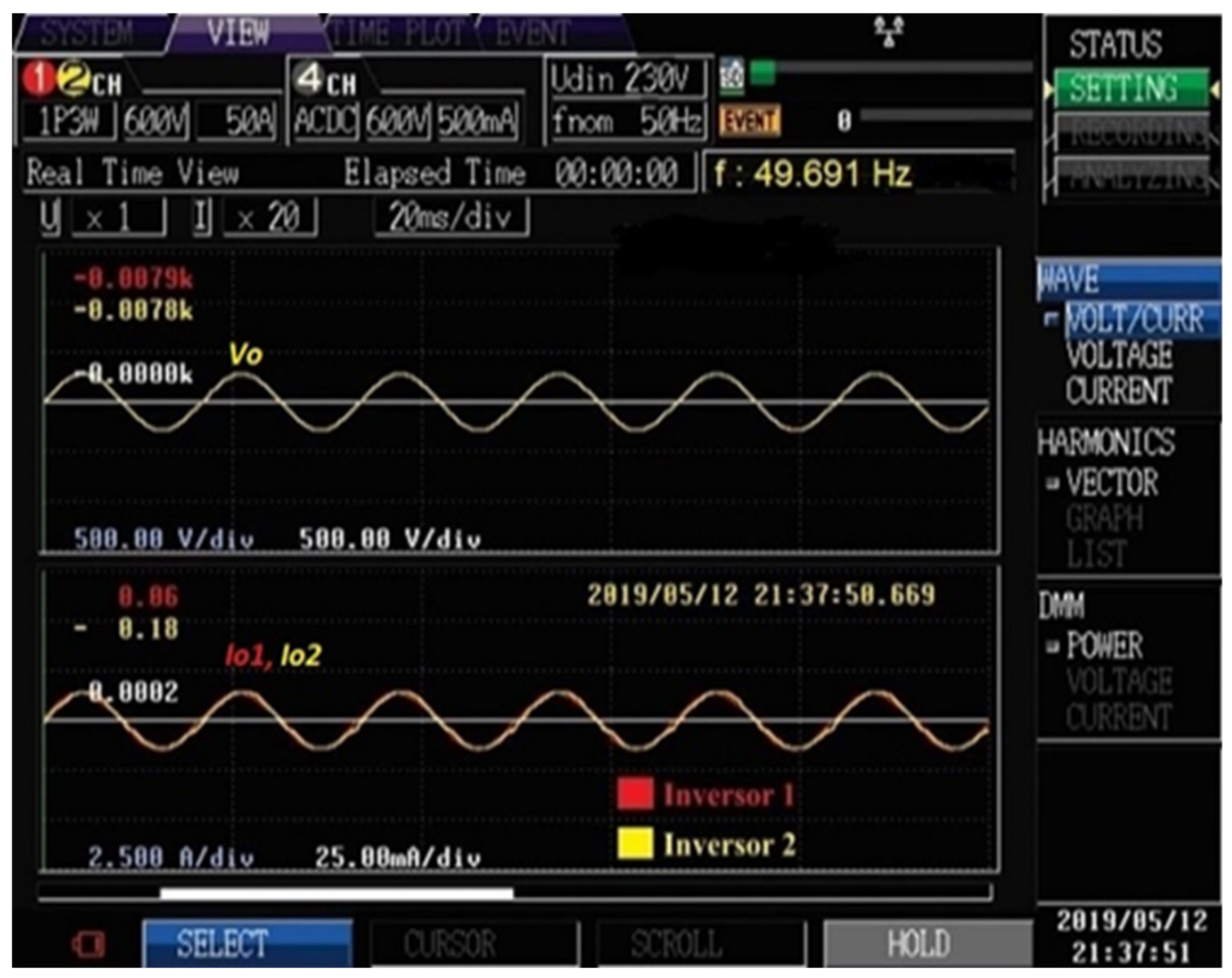
Figure 26, PW3198, the HIOKI network analyzer was used to display the voltage and current waveforms of two inverters connected in parallel, feeding a 170 Ω resistive load. This graph shows that the two inverters share the load in a homogeneous way, supplying currents of the same intensity with values close to 1.9 A. RMS, which justifies that both inverters are synchronized and in phase. Additionally, it is observed how the voltage signal maintains its amplitude with a value close to 230 V RMS, with a sinusoidal waveform, which proves the good performance of the designed controllers.

8. Results Discussion

This work presents the design and development of two control techniques for the grid-disconnected mode operation of an inverter. The objective of these two controllers is to provide better disturbances rejection when the converter supplies both linear and non-linear local loads. With its implementation through simulations and experimental tests, total harmonic distortion values were obtained in the voltage signal (THDv) between 1.0% and 2.5%, which represents an effective performance considering the recommendations of the IEEE 519-1992 standard, which must be less than 5%. Likewise, the parallel connection of power converters is effectively ensured. The simulations show that, at the time of interconnection and in the event of load changes, the transients present are less than 20% above the reference. Regarding the works presented in the literature, it is evident that different authors propose control strategies to reduce harmonic distortion with results close to those found in this work (THDv = 2%). Other authors propose strategies that allow the parallel connection of energy conversion units presented, with good performance. However, in this work, both strategies are proposed and implemented; that is, solutions for both the parallel connection of converters and regulators for the reduction of THDv, when the converter feeds linear and non-linear loads.
The 2DOF + RC is more robust than a repetitive controller considering that the former is designed with two controllers, one for the direct loop, and one for the feedback loop. Particularly, in the feedback loop, a controller is designed to provide larger system disturbances rejection, and the other, in the direct loop, is designed to have good setpoint tracking and contribute to the disturbance rejection task, in contrast with less robust repetitive control schemes that are normally designed in the direct loop.
The PI-P + ResC control configuration consists of two controllers: a PI + ResC controller for the direct loop and another P controller for the feedback loop. Particularly, the PI + ResC controller is designed for good setpoint tracking and the P controller for better disturbances rejection. Therefore, this control structure turns out to be more robust and presents better performance than a resonant controller, which is normally designed for direct control loop.

9. Conclusions

In the literature, control configurations have been applied to solve harmonic distortion problems for both current and voltage signals in converter applications operating in grid-connected and islanded modes. Some of these works use control configurations like resonant, repetitive, PID, control of sliding modes, and others, performing within the regulations aforementioned. In this work, two control configurations are developed and applied. The first one is configured with a control of two-degrees-of-freedom plus a repetitive control (2DOF + RC), and the second is configured with a proportional integral–proportional control plus a resonant control (PI-P + ResC). Both configurations are a new proposal in the suitable solution for problems of reduction of harmonic distortion and parallel inverter connection. These configurations combine two different control schemes in their structure to improve upon their performance. What characterizes both configurations is that a controller is implemented in the direct loop and another controller in the feedback loop, which allows to improve the performance of the converter, presenting an adequate set point tracking and, at the same time, improving the system disturbance rejection. Specifically, both control configurations allow for a steady state error equal to zero (eee = 0) and the disturbance rejection with linear and non-linear load is in the range between 1% and 2.5%, below the recommended by regulations IEEE 519-1992, which is 5%. In particular, by means of the implementation through simulations and experimental tests presented in this work, good performance of the system is justified, considering that with the implementation of these regulators, it is possible to have good set point tracking and good disturbances rejection. This causes the amplitude of the voltage signal to present values close to 230 V RMS, at 50 Hz. Additionally, inverters are successfully paralleled in response to increases in load demand. The reference voltage signal is obtained through droop schemes that allow the inverters connection in parallel to meet increases in load demand. Particularly, for this application, a resistive droop scheme was chosen with a virtual impedance loop of the same characteristics that allows the inverters parallel connection and the homogeneous distribution of active and reactive power demanded by the load. Their choice was determined considering that with the implementation of both controllers, the inverter closed-loop impedance presents a resistive characteristic.
The controller showed the capacity to reduce the Total Harmonic Distortion (THDv) of the inverter’s output below the 5% recommended by the IEEE 519-1992. THDv values of 1.2, 2.2, and 2.5% were obtained for in-parallel connected inverters feeding either a linear or non-linear load. It is worth noticing that if the PI-P + ResC controller is implemented, it is not necessary to use a virtual impedance loop.
In this work, methods are specifically described and developed so that experts in this area of knowledge can implement with certainty control strategies that allow improving the disturbances rejection in power electronic converters. Particularly, as already mentioned, for converter island mode operation. In addition, the criteria and strategies are established to effectively carry out the parallel connection of converters to meet load demands.

Author Contributions

Conceptualization, R.O. and J.C.S.-S.; methodology, J.C.S.-S.; software, V.H.G.; validation, R.O., J.J.R. and V.V.; formal analysis, R.O.; investigation, R.O.; resources, A.L.G.-G.; data curation, R.O.; writing—original draft preparation, R.O.; writing—review and editing, A.L.G.-G.; visualization, J.C.S.-S.; supervision, J.C.S.-S.; project administration, J.C.S.-S.; funding acquisition, J.C.S.-S. All authors have read and agreed to the published version of the manuscript.

Funding

This research received no external funding.

Data Availability Statement

Data available in a publicly accessible repository.

Acknowledgments

The authors gratefully recognize financial support from Instituto Politécnico Nacional through grant SIP1822 and the COFAA-IPN.

Conflicts of Interest

The authors declare no conflict of interest.

References

  1. Trebolle, D.; Gómez, T. Reliability Options in Distribution Planning Using Distributed Generation. IEEE Lat. Am. Trans. 2010, 8, 557–564. [Google Scholar] [CrossRef]
  2. Carballo, R.; Nunez, R.; Kurtz, V.H.; Botteron, F. Design and Implementation of a Three-Phase DC-AC Converter for Microgrids Based on Renewable Energy Sources. IEEE Lat. Am. Trans. 2013, 11, 112–118. [Google Scholar] [CrossRef]
  3. Del Carpio Huayllas, T.E.; Ramos, D.S.; Vasquez Arnez, R.L. Microgrid Systems: Main Incentive Policies and Performance Constraints Evaluation for their Integration to the Network. IEEE Lat. Am. Trans. 2014, 12, 1078–1085. [Google Scholar] [CrossRef]
  4. Trujillo, C.L.; Velasco, D.; Figueres, E.; Garcerá, G. Analysis of active islanding detection methods for grid-connected microinverters for renewable energy processing. Appl. Energy 2010, 87, 3591–3605. [Google Scholar] [CrossRef] [Green Version]
  5. Gomez, J.C.; Vaschetti, J.; Coyos, C.; Ibarlucea, C. Distributed Generation: Impact on Protections and Power Quality. IEEE Lat. Am. Trans. 2013, 11, 460–465. [Google Scholar] [CrossRef]
  6. The Institute of Electrical and Electronics Engineers. IEEE STD 519-1992. IEEE Recommended Practices and Requirements for Harmonic Control in Electric Power Systems; The Institute of Electrical and Electronics Engineers: New York, NY, USA, 1993; ISBN 1-55937-239-7. [Google Scholar]
  7. Converters, S.P. IEEE Guide for Harmonic Control and Reactive Compensation of Static Power Converters; IEEE: Piscataway, NJ, USA, 1981. [Google Scholar]
  8. Hossain, M.A.; Pota, H.R.; Hossain, M.J.; Blaabjerg, F. Evolution of microgrids with converter-interfaced generations: Challenges and opportunities. Int. J. Electr. Power Energy Syst. 2019, 109, 160–186. [Google Scholar] [CrossRef]
  9. Baek, S.; Cho, Y.; Yeo, S. Improved Voltage Control Scheme for Single-Phase UPS Inverter with Repetitive Current Controller. In Proceedings of the 2019 IEEE Energy Conversion Congress and Exposition (ECCE), Baltimore, MD, USA, 29 September–3 October 2019; pp. 1482–1487. [Google Scholar] [CrossRef]
  10. Jamil, M.; Waris, A.; Gilani, S.O.; Khawaja, B.A.; Khan, M.N.; Raza, A. Design of Robust Higher-Order Repetitive Controller Using Phase Lead Compensator. IEEE Access 2020, 8, 30603–30614. [Google Scholar] [CrossRef]
  11. Jank, H.; Venturini, W.A.; Meurer, A.P.; Bisogno, F.; Martins, M.L.S.; Rech, C. Comparative analysis of PID, resonant and repetitive controllers applied to a single-phase PWM inverter. In Proceedings of the 2017 Brazilian Power Electronics Conference (COBEP), Juiz de Fora, Brazil, 19–22 November 2017; pp. 1–6. [Google Scholar]
  12. Chen, W.; Cai, F.; Lin, Q.; Wang, W. Improved PI and Repetitive Controller for Dual-Buck Inverter. In Proceedings of the 2020 39th Chinese Control Conference (CCC), Shenyang, China, 27–29 July 2020; pp. 6157–6161. [Google Scholar]
  13. Chen, Z.; Zha, H.; Peng, K.; Yang, J.; Yan, J. A Design Method of Optimal PID-Based Repetitive Control Systems. IEEE Access 2020, 8, 139625–139633. [Google Scholar] [CrossRef]
  14. Pan, Z.; Dong, F.; Zhao, J.; Wang, L.; Wang, H.; Feng, Y. Combined Resonant Controller and Two-Degree-of-Freedom PID Controller for PMSLM Current Harmonics Suppression. IEEE Trans. Ind. Electron. 2018, 65, 7558–7568. [Google Scholar] [CrossRef]
  15. Patil, T.D.; More, D.S. Comparative analysis of Cuk converter with proportional integral controller & proportional resonant controller. In Proceedings of the 2019 International Conference on Communication and Electronics Systems (ICCES), Coimbatore, India, 17–19 July 2019; pp. 1654–1659. [Google Scholar]
  16. Sreekumar, P.; Danthakani, R.; Veettil, S.P. Implementation of proportional-resonant controller in an autonomous distributed generation unit. In Proceedings of the 2018 Advances in Science and Engineering Technology International Conferences (ASET), Abu Dhabi, UAE, 6 February–5 April 2018; pp. 1–5. [Google Scholar]
  17. Torres, A.P.; Roncero-Sánchez, P.; Batlle, V.F. A Two Degrees of Freedom Resonant Control Scheme for Voltage-Sag Compensation in Dynamic Voltage Restorers. IEEE Trans. Power Electron. 2018, 33, 4852–4867. [Google Scholar] [CrossRef]
  18. Iricik, S.; Komurcugil, H. Proportional-Integral and Proportional-Resonant Based Control Strategy for PUC Inverters. In Proceedings of the IECON 2018—44th Annual Conference of the IEEE Industrial Electronics Society, Washington, DC, USA, 21–23 October 2018; pp. 3369–3373. [Google Scholar]
  19. Kishan, V.K.; Puthra, P.P.; Reddy, K.N. Paralleling of inverters with dynamic load sharing. In Proceedings of the 2016 IEEE 7th Power India International Conference (PIICON), Bikaner, India, 25–27 November 2016; pp. 1–6. [Google Scholar] [CrossRef]
  20. Raj, D.C.; Gaonkar, D.N. Frequency and voltage droop control of parallel inverters in microgrid. In Proceedings of the 2016 2nd International Conference on Control, Instrumentation, Energy & Communication (CIEC), Kolkata, India, 28–30 January 2016; pp. 407–411. [Google Scholar] [CrossRef]
  21. Sarvghadi, P.; Monfared, M. Load sharing control of parallel inverters with uncertainty in the output filter impedances for islanding operation of AC micro-grid. In Proceedings of the 2017 Conference on Electrical Power Distribution Networks Conference (EPDC), Semnan, Iran, 19–20 April 2017; pp. 55–61. [Google Scholar] [CrossRef]
  22. Araki, M.; Taguchi, H. Tutorial Paper Two-Degree-of-Freedom PID Controllers. Int. J. Control Autom. Syst. 2003, 1, 4. [Google Scholar]
  23. Broberg, H.L.; Molyet, R.G. Reduction of repetitive errors in tracking of periodic signals: Theory and application of repetitive control. First IEEE Conf. Control Appl. 1992, 2, 1116–1121. [Google Scholar]
  24. Ogata, K.; Yang, Y. Modern Control Engineering, 4th ed.; Prentice Hall: Upper Saddle River, NJ, USA, 2001. [Google Scholar]
  25. PSIM 7.0, Users Guide; Powersim Inc.: Maryland, MD, USA, 2006.
  26. Mohan, N.; Underland, T.M.; Robbins, W.P. Power Electronics: Converters, Applications, and Design, 3th ed.; John Wiley & Sons: Hoboken, NJ, USA, 2003. [Google Scholar]
  27. Vorperian, V. Simplified analysis of PWM converters using model of PWM switch. II. Continuous conduction mode. IEEE Trans. Aerosp. Electron. Syst. 1990, 26, 490–496. [Google Scholar] [CrossRef]
  28. Zmood, D.N.; Holmes, D.G. Stationary frame current regulation of PWM inverters with zero steady-state error. IEEE Trans. Power Electron. 2003, 18, 814–822. [Google Scholar] [CrossRef]
  29. Benavent, J.M.; Figueres, E.; Garcera, G.; Pascual, M. Robust model-following regulator for average current-mode control of boost DC-DC converters. In Proceedings of the IEEE International Symposium on Industrial Electronics, Dubrovnik, Croatia, 20–23 June 2005; Volume 2, pp. 715–720. [Google Scholar]
  30. Ortega Gonzalez, R.; Sosa Saavedra, J.C.; Carranza Castillo, O.; Garcia Ortega, V. Comparison controllers for inverter operating in island mode in microgrids with linear and nonlinear loads. IEEE Lat. Am. Trans. 2014, 12, 1441–1448. [Google Scholar] [CrossRef]
  31. Kawabata, T.; Higashino, S. Parallel operation of voltage source inverters. IEEE Trans. Ind. Appl. 1988, 24, 281–287. [Google Scholar] [CrossRef]
  32. Guerrero, J.M.; de Vicuña, L.G.; Matas, J.; Miret, J.; Castilla, M. Output impedance design for parallel-connected UPS inverters. In Proceedings of the IEEE International Symposium on Industrial Electronics (ISIE’04), Ajaccio, France, 4–7 May 2004. [Google Scholar]
  33. Jensen, U.B.; Blaabjerg, F.; Enjeti, P.N. Sharing of nonlinear load in parallel connected three-phase converters. In Proceedings of the IEEE Industry Applications Annual Meeting (IAS’00), Rome, Italy, 8–10 October 2000; Volume 4, pp. 2338–2344. [Google Scholar]
  34. Zhong, Q.C.; Blaabjerg, F.; Guerrero, J.M.; Hornik, T. Reduction of voltage harmonics for parallel-operated inverters. In Proceedings of the IEEE Energy Conversion Congress and Exposition, Phoenix, AZ, USA, 17–22 September 2011; pp. 473–478. [Google Scholar]
  35. Borup, U.; Blaabjerg, F.; Enjeti, P.N. Sharing of nonlinear load in parallel-connected three-phase converters. IEEE Trans. Ind. Appl. 2001, 37, 1817–1823. [Google Scholar] [CrossRef]
  36. Guerrero, J.M.; Berbel, N.; Matas, J.; de Vicuna, L.G.; Miret, J. Decentralized Control for Parallel Operation of Distributed Generation Inverters in Microgrids Using Resistive Output Impedance. In Proceedings of the 32nd Annual Conference on IEEE Industrial Electronics, IECON, Paris, France, 6–10 November 2006; pp. 5149–5154. [Google Scholar]
  37. Guerrero, J.M.; de Vicuña, L.G.; Matas, J.; Miret, J.; Castilla, M. Output impedance design of parallel-connected UPS inverters with wireless load-sharing control. IEEE Trans. Ind. Electron. 2005, 52, 1126–1135. [Google Scholar] [CrossRef]
Figure 1. Inverter schematic.
Sustainability 13 05115 g001
Figure 2. Small signal model of inverter.
Sustainability 13 05115 g002
Figure 3. LC filter scheme.
Sustainability 13 05115 g003
Figure 4. Control scheme diagram.
Sustainability 13 05115 g004
Figure 5. Bode diagram of inverter current loop.
Sustainability 13 05115 g005
Figure 6. Block diagram for 2DOF + RC control. The current loop is closed.
Sustainability 13 05115 g006
Figure 7. Bode diagram of the voltage loop using 2DOF + CR and PI + RC controller.
Sustainability 13 05115 g007
Figure 8. Block diagram for PI-P + ResC.
Sustainability 13 05115 g008
Figure 9. Bode diagram of the voltage loop using PI-P + ResC and PI + ResC controller.
Sustainability 13 05115 g009
Figure 10. Small-signal model and block diagram of the closed loop system.
Sustainability 13 05115 g010
Figure 11. Bode diagram of the closed loop impedance Zo_lc with 2DOF + RC controller.
Sustainability 13 05115 g011
Figure 12. Bode diagram of the closed loop impedance Zo_lc with PI-P + ResC.
Sustainability 13 05115 g012
Figure 13. Schematic of two inverters connected in parallel.
Sustainability 13 05115 g013
Figure 14. Waveforms of the current and voltage signal obtained with the PI + RC controller implementation in the voltage loop.
Sustainability 13 05115 g014
Figure 15. Waveforms of the current and voltage signal, obtained with the PI-P + ResC controller implementation in the voltage loop.
Sustainability 13 05115 g015
Figure 16. Waveforms of the current and voltage signal, obtained with the PI + RC controller implementation in the voltage loop.
Sustainability 13 05115 g016
Figure 17. Waveforms of the current and voltage signal, obtained with the 2DOF + RC controller implementation in the voltage loop.
Sustainability 13 05115 g017
Figure 18. 2DOF + RC controller waveforms. From top to bottom: voltage, current, and power output of the inverters, with voltage loop and feeding resistive load.
Sustainability 13 05115 g018
Figure 19. 2DOF + RC controller waveforms. From top to bottom: voltage, current, and power output of the inverters, with voltage loop, feeding resistive load and THDv = 1.2%.
Sustainability 13 05115 g019
Figure 20. 2DOF + RC controller waveforms. From top to bottom: voltage, current, and power output of the inverters, with voltage loop and feeding nonlinear load.
Sustainability 13 05115 g020
Figure 21. 2DOF + RC controller waveforms in detail, of Figure 15. From top to bottom: voltage, current, and power output of the inverters, in the time scale (6 to 6.2) and THDv = 2.1%.
Sustainability 13 05115 g021
Figure 22. PI-P + ResC controller waveforms. From top to bottom: voltage, current, and power output of the inverters, with voltage loop and feeding non-linear loads.
Sustainability 13 05115 g022
Figure 23. PI-P + ResC controller waveforms. From top to bottom: voltage, current, and power output of the inverters, with voltage loop and feeding non-linear loads, THDv = 2.5%.
Sustainability 13 05115 g023
Figure 24. Inverter output voltage with nonlinear load, R2DOF (top, 200 V/div) and Inverter output current with nonlinear load, 2DOF+RC control (bottom, 1 A/div). Time scale = 5 ms/div. THDv = 2.2%.
Sustainability 13 05115 g024
Figure 25. Inverter output voltage with nonlinear load, PI-P + ResC control (top, 200 V/div) and Inverter output current with nonlinear load, PI-P + ResC control (bottom, 1 A/div). Time scale = 5 ms/div. THDv = 2.6%.
Sustainability 13 05115 g025
Figure 26. Waveforms of Output voltage vO (first graph, 500 V/div), and output current of two inverters connected in parallel in grid-disconnected operation io (second graph, 3 A/div).
Sustainability 13 05115 g026
Table 1. Inverter Main Parameters.
ParameterValue
Nominal power of the inverter ( P )440 W
DC_LINK voltage ( V DC )400 V
Inverter output voltage ( V o )230 VRMS
Inverter output frequency ( f o )50 Hz
Inverter output inductance ( L )9.57 mH
Inverter Output capacitor ( C )600 nF
Damping resistance ( R d )5 Ω
Inverter switching frequency ( f s )20 kHz
Load resistance ( R Load )170 Ω
Table 2. Resonant controller parameters.
Harmonic K h B h
1K150B12·π·0.3
3K335B32·π·0.9
5K520B52·π·1.5
7K720B72·π·2.1
9K920B92·π·2.7
11K1120B112·π·3.3
Table 3. Inverter Output Voltage THDv.
ControllerLoadTHDv (%)
2DOF + RCNonlinear2.2
PI-P + ResCNonlinear2.6
Publisher’s Note: MDPI stays neutral with regard to jurisdictional claims in published maps and institutional affiliations.

