Abstract
This article investigates the potential environmental impacts of four-layer printed circuit board (PCB) production from cradle to grave. The study starts with a lifecycle assessment of conventional PCB production. Then, the alternative materials of polyethylene terephthalate (PET), polylactic acid (PLA)/glass fiber composite and paper are investigated for the substrate. A conventional PCB adopts copper as the conductive material and requires an etching process. The environmental impacts of changing the conductive deposition method to an additive method by printing silver nanoparticles is studied. In a conventional PCB, electricity generation contributes 41% of the global warming potential (GWP) and 38% of the abiotic resource depletion (ADP), in the fossil category. By applying an additive manufacturing method, the GWP of PCB manufacturing can be reduced to 14% of that of the conventional method. A sensitivity analysis of silver recycling illustrates that a 40% higher silver recycling rate would decrease the GWP of silver material by about 48–60%. Uncertainty in the energy consumption of PCB production would alter the environmental impacts; however, even with the most conservative energy consumption in a conventional PCB production method, the environmental impacts of the additive method are about five times lower than those of conventional PCB production.
1. Introduction
By 2021, the market for the Internet of Things (IoT) has been forecast to expand to billions of devices [1], which will consequently produce a considerable amount of electronic waste. One requirement of digitalization is that electronics are embedded in products, which, at some point in their lifecycle, may be released into the natural environment. Examples of applications for embedded electronics include sensors in disposable smart packaging, flexible and printable electronics embedded in consumer products, health care products and disposable sensors for weather and crop monitoring. On the other hand, the increasing amount of electronic equipment increases the environmental impacts of their materials and production.
New trends and applications in the electronic industry require novel developments and the re-designing of sustainable alternatives to the existing production stream. This new market opens a discussion on how conventional practices in electronics manufacturing are in accordance with the sustainability principles and how the environment may benefit from the transformation of production practices in the electronics industry.
Printed circuit boards (PCBs) are a fundamental component in almost all electronic products, and circuits, devices and chips are built on PCBs. Conventional multilayer PCBs consist of a core dielectric layer (substrate) clad with copper as a conductive material on both sides and laminated with several layers of prepreg and copper foil by applying a high pressure and temperature [2]. Chemical resists with printed circuit patterns are deposited on the conductive layer. The copper surface is exposed to chemicals and the extra copper is removed by chemical etching [3].
The substrate of PCB, most commonly known as flame retardant (FR4), is a composite material consisting of three main components: epoxy resin, woven glass fiber (GF) and copper foil [3]. Epoxy resin is derived from non-renewable crude oil. The manufacturing process of GF is energy-intensive, and the copper preparation method requires the use of extensive energy and solvents [4].
Bio-based materials, as a substrate of consumer electronics, could embrace the requirements of embedded electronics such as being flexible, lightweight, printable and low-cost, while enhancing the environmental profile of these products by incorporating biodegradability and composability, and decreasing the energy and materials used in their production. The utilization of flexible and bio-based composites to produce PCB substrates has led many researchers to study the feasibility of eco-friendly alternative substrates. The authors of [2] investigated the application of lignin incorporated into a brominated epoxy matrix. The authors of [5] studied the application of epoxidized linseed oil obtained from flax plants, combined with a small portion of conventional epoxy resin (bisphenol-F). The authors of [6] investigated the environmental impacts of paper-based multilayer PCB. The authors of [7] utilized polylactic acid (PLA) as the substrate of PCB. The authors of [8] investigated the utilization of polyethylene terephthalate (PET) as the substrate of flexible PCB. However, there is a lack of studies on the environmental impacts of the new generation of printed and flexible PCBs on substrates such as PET and PLA composites. PLA is produced from pure renewable materials, such as corn and sugar beets [9], and is considered a biodegradable polymer for developing sustainable and environmentally friendly electronics [7]. PLA is mostly applied in food packaging at present, either as a bottle for liquids [10] or as a thin film [11]. There are few scientific articles regarding the fabrication of electronic devices on PLA substrates, since the glass transition temperature of PLA is very low (Tg = 58 °C), which implies significant constraints on the manufacturing of electronics, where the substrate is usually exposed to higher temperatures [12,13,14].
The improvement of the mechanical and thermal properties of PLA has attracted the attention of many researchers. The main cause of the poor mechanical and thermal performance of PLA is PLA’s poor crystallization abilities [15]. Glass fiber is the most common synthetic material utilized to reinforce polymers, due to its excellent mechanical and heat-resistance performance [16].
Electrically conductive adhesives (ECAs) have been widely applied in electronic research and development and the functionalities of ECA for applications on paper, PET and PLA have been proven [17]. There are several possible options for the conductive ink used for PCBs. The goal of this study was not to compare different conductive inks. AgNP was selected as the ink, since experimental results from the literature and other studies in the ongoing research project showed the feasibility of using AgNP as the printing ink [18,19,20,21]. This study adopted silver nanoparticles (Ag NPs) and thermoset polyurethane as the ECA and screen printing as the deposition method.
Material recovery from disposed PCBs is an important issue since old PCBs contain valuable materials and may endanger the environment if they are not managed properly. Thus, several recycling and recovery processes have been developed to close the loop in PCB production [22]. A sensitivity analysis of silver recovery is included in this study to examine the importance of proper waste treatment.
The aim of the current study is to fill the literature gap of a cradle-to-grave lifecycle assessment (LCA) to assess and compare the environmental impacts of a novel trend in the green and flexible electronic industry. The current article quantifies the environmental impacts of PCB production and demonstrates the benefit of moving from subtractive manufacturing to additive manufacturing.
2. Materials and Methods
The current article is part of the ECOtronics project, in which different research units investigate the electrical circuits, material behavior and commercial aspects of developing printed electronics. The objective of this study is to demonstrate the potential of printed electronics to decrease the environmental impacts throughout the products’ lifecycle. The scenarios in this article were based on the best commercially available materials and could help electronic circuit designers to understand the environmental profile of their products.
The data used to conduct a lifecycle assessment were gathered by searching through the following sources:
- (1)
- LCA databases (Ecoinvent database or GaBi software);
- (2)
- Literature study;
- (3)
- Contacting specialists in the field.
A lifecycle assessment (LCA) quantifies the potential environmental impacts throughout the products’ lifecycle [23]. The LCA framework is implemented in four phases: goal and scope definition, lifecycle inventory (LCI), lifecycle impact assessment (LCIA) and interpretation. In addition, a sensitivity analysis is recommended to enhance the creditability of the LCA study [23].
2.1. Goal and Scope Definition
The goal of this LCA study was to assess and compare the environmental impact of alternative production methods and materials for PCB manufacturing. The conventional substrate in this study refers to fiber-glass-reinforced brominated epoxy resin (FR4) and the comparative cases are PET, PLA/GF composite and paper. The conductive material in the baseline is copper and, in other cases, the baseline is an electrically conductive adhesive, which is a combination of 50% resin and 50% silver nanoparticles.
The manufacturing method for the baseline scenario is conventional copper treatment (chemical etching is involved), and, in the other cases, the method is lab-scale PCB production, which is mainly based on the experimental procedure described in [6].
The functional unit in this LCA study was set as one m2 of four-layer PCB. The thickness of the conventional PCB substrate is 1.6 mm, whereas, for the alternative cases, the thickness of the substrate material was retrieved from [8], which has two layers of 125 µm and one layer of 36 µm.
The system boundary of this study is depicted in Figure 1, covering cradle-to-grave processes. It includes the raw material acquisition, manufacturing, and waste disposal of PCB. Transport and use phases are excluded from the system boundaries because they are assumed to be the same for all alternatives. Most of the utilized data represent global conditions; however, due to the lack of global data, some data sources correspond to more specific geographical locations.
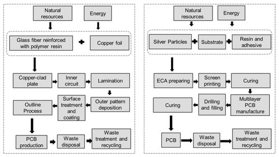
Figure 1.
System boundaries of study, baseline scenario (left) and alternative PCB scenarios (right).
Scenario Description
Several possible alternative materials were studied for the PCB substrate. PET, PLA/GF and paper were selected in this study, and etched copper was substituted with ECA containing silver nanoparticles (Ag NPs). Five study scenarios are listed in Table 1.

Table 1.
Scenarios for PCB production.
S1 represents the baseline scenario for a conventional FR4-based PCB, and S2 is a hypothetical scenario designed to check the environmental impacts when only the conductive material is changed to Ag NPs. The intention of introducing S2 was to demonstrate the environmental benefits when only the manufacturing process (not the substrate material) is changed from a subtractive method to an additive method. Then, in scenarios S3, S4 and S5, the substrate material is also changed. In S2–S5, Ag NPs were utilized as the conductive material, deposited on the substrate using the screen-printing method. S3 represents a scenario related to the PET-based substrate. S4 depicts the scenario derived from the PLA/GF composite. The substrate material in scenario S5 is normal printing paper.
From the functional perspective, the function of S3, S4 and S5 is, to some extent, different; PET plastic is applicable, whereas a transparent substrate is needed. PLA/GF is a bio-compostable plastic and would be used in bioplastic packaging. Using paper as the substrate has the advantage of biodegradability and is suitable in paper and cardboard packaging. The objective of this article was not to compare different substrate materials, but to show the environmental impacts of moving toward sustainable electronics.
2.2. Lifecycle Inventory (LCI)
LCI is an LCA stage quantifying the inputs and outputs of the studied system, and is performed for each scenario. Table 2 shows the data source for each unit process. The LCIs for processes in Scenarios 1 and 2 were mainly obtained from the Ecoinvent 3.6 database, with the activity name “printed wiring board production, for surface mounting, Pb free surface”. This process represents the manufacturing of 1 m2 of a six-layer PCB based on the FR4 substrate. The dataset was compiled using the data collected during 2003–2006 from environmental reports of three PCB manufacturers in Europe and it covers the manufacturing processes of a printed wiring (circuit) board: raw materials, energy consumption, emission to air and water and waste amount from the production of 1 m2 of PCB [24].

Table 2.
Inventory data of the studied unit processes.
The literature has reported controversial results regarding the electricity and heat consumption involved in the manufacturing of conventional FR4-based PCBs (S1 and S2). The electricity and heat consumption values in the Ecoinvent database for a six-layer PCB are 326 and 105 kWh. The authors in [6] collected the inventory data from a manufacturing plant in China and reported a total energy consumption for the manufacturing process of 20 kWh. The authors in [25] collected the inventory data from a manufacturing plant in Turkey and reported the total energy consumption for the manufacturing process of 1 m2 of a 2-layer PCB as 7.15 kWh. The authors in [5] reported the energy consumption of a 1 m2 PCB substrate (only the FR4) as 13.4 kWh. The authors in [26] studied the energy consumption of PCB manufacturing and calculated the energy demand for each unit process of a four-layer PCB production. They reported the total energy demand for the manufacturing of a panel of a 4-layer PCB as about 6 kWh. Considering the typical size of a PCB panel (18 × 24”, 18 × 21”, 21 × 24”) [27], the energy demand for 1 m2 of a 4-layer PCB would be 18–25 kWh. Therefore, in Scenario 1 of this study, the total energy consumption for manufacturing 1 m2 of a 4-layer PCB is assumed to be 20 kWh and, in Scenario 2, 10 kWh is taken as the electricity consumption. To assess the impact of uncertainty regarding this parameter on the results, a sensitivity analysis was carried out.
As mentioned above, the functional unit of this study was set to 1 m2 of a four-layer PCB. However, in the Ecoinvent database, LCI only exists for a two-layer and six-layer PCB. Thus, it is necessary to convert the inventory dataset of a 6-layer PCB into a four-layer PCB. The structures of the multilayer PCBs produced by different manufacturers are roughly similar. As an example, the researchers in [28] described the structure of typical four- and six-layer PCBs. The quantity of sheet rolling and the mass of copper used in the dataset for a six-layer PCB was modified by factor of 66% to represent the inventory to produce 1 m2 of a four-layer PCB.
The inventory data for the manufacturing of a PCB in Scenarios 3–5 were mainly obtained from [6], since, at the date of this study, [6] is the only article which reported a full inventory of materials and energy consumption for the manufacturing of a multilayer PCB based on a paper substrate. In Scenarios 3 and 4, the thickness of substrates was retrieved from [8] and the weight of each material in the substrate was calculated using the average density of 1.38 g/cm3 and 1.5 g/cm3 for PET and PLA/GF substrates, respectively.
The waste management of a conventional PCB is a complicated and multi-process procedure, and an environmental impact assessment of the end-of-life (EoL) stage of a conventional PCB is not the focus of this study. Therefore, in Scenarios 1 and 2, the environmental impact corresponding to Scenario 1 of [29] is imported to the model in the GaBi program. In the EoL stage of the other scenarios, it is assumed that 50% of the silver contained in the used PCB can be separated and recycled [30], and the rest of the PCB material is incinerated. In Scenarios 3, 4 and 5, for the purposes of modeling, each material fraction of PCB (PET, resin, paper, PLA and GF) was modeled separately in its corresponding incineration unit process.
The authors in [31] studied the possible routes for the manufacturing of silver nanoparticles. Ag NPs are produced through several synthesis methods with different reactions, inputs and particle sizes. The authors in [32] conducted a comprehensive LCA study for various Ag NPs’ production routes. They selected three production methods of chemical reduction with trisodium citrate (CR-TSC) as applicable for the electronics industry. The inventory data regarding the manufacturing of Ag NPs were taken from [31].
2.3. Lifecycle Impact Assessment (LCIA)
LCA studies were carried out in GaBi 9 software. The CML 2001—August 2016 method was selected to assess the environmental impacts. The selected environmental impact categories used to assign LCI results to specific environmental issues were as follows: Abiotic Depletion Potential (ADP) (fossil), Acidification Potential (AP), Eutrophication Potential (EP), Freshwater Aquatic Ecotoxicity Potential (FAETP), Global Warming Potential (GWP), Human Toxic Potential (HTP), Ozone Layer Depletion Potential (ODP), Photochemical Ozone Creation Potential (POCP) and Terrestrial Eco-toxicity Potential (TETP). These categories can describe the environmental impact of PCB production.
3. Results
The results presented in Figure 2 are based on the environmental assessment of each scenario described in the lifecycle inventory section. They depict the environmental impacts for all impact categories. S1 has the highest environmental impacts in all categories. Comparing the environmental impacts of S1 with S3, S4 and S5 in all impact categories, the additive manufacturing of PCBs using AgNPs and PET, PLA/GF and paper as substates has less than 80% of the impact of the baseline scenario. The primary reason for the lower impacts in the latter scenarios stems from the simplicity of the inventory used in S3, S4 and S5, and the lower material intake. For instance, about 2.87 kg of copper was consumed to manufacture 1 m2 of the baseline PCB. However, in S3, S4 and S5, only 0.0103 kg of AgNPs was used. Furthermore, in S1, several chemical substances were consumed, mainly for the treatment of etched copper. Finally, S1 follows the subtractive method, which is energy-intensive and consumes a large amount of chemicals, whereas scenarios S3, S4 and S5 follow the additive method, which is material-efficient and requires considerably less energy. The environmental impacts of scenarios S3, S4 and S5 in all the categories are almost equal, and the variation is within the range of 4% of the S1 amount. In ADP fossil and GWP categories, S2 has a 48% and 49% lower impact. Scenario S2 has the same substrate as S1; thus, by changing the material from copper to silver nanoparticles, there would be a greater than 50% decrease in the environmental impacts of S1.
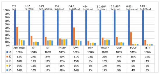
Figure 2.
Lifecycle comparison of five scenarios based on the impact categories of CML 2001—August 2016. Numbers on top of bars indicate the absolute value for S1 in each impact category.
Figure 2 shows the relative environmental impacts of these scenarios and is suitable for comparing the scenarios; however, a contribution analysis sheds light onto the reasons for the different impacts of the scenarios. Figure 3 shows the contribution of different processes and materials to the environmental impacts of each scenario. The vertical axis corresponds to the share of each process from the total environmental impacts. The absolute value of the environmental impacts for each process is also denoted in Figure 3. The inventory processes are aggregated into four groups of “Electricity”, “Conductive”, “Substrate” and “Chemicals” to distinguish the contribution of each group of materials. The “Electricity” group represents the electricity consumption for each manufacturing scenario; the “Conductive” group corresponds to the processes related to conductive metal, which in S1 is copper use and in S2, S3, S4 and S5 is silver from the raw material intake; and the material deposition to the EoL stage.
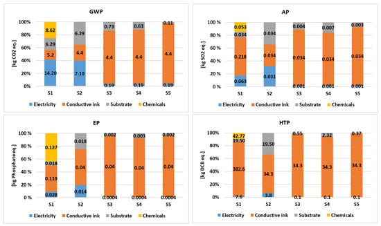
Figure 3.
Contribution of inventories in LCIA. The vertical axis corresponds to the share of each process from the total environmental impacts and the number on each bar indicates the absolute value of the environmental impacts.
The “Chemicals” group in S1 represents the unit processes of iron(III)chloride, sodium chloride, sodium hydroxide, water, hydrogen peroxide, sulfuric acid, dipropylene glycol monomethyl ether and hydrochloric acid. These substances are mainly consumed during etching and copper recovery at the production plant. The “Substrate” group represents the materials incorporated in the substrate of PCBs. Figure 3 demonstrates the aggregated environmental impacts of both the production and EoL stages for substrate and conductive groups.
In Scenario 1, electricity is the main contributor to GWP, at 41%, followed by chemical processes in manufacturing and the FR4 substrate. However, in EP and AP, copper treatment and chemicals are the main sources of emissions.
In Scenarios 3, 4 and 5, the conductive material (Ag NPs) is the most significant contributor in all environmental impact categories, even though it accounts for less than 3% of the total substrate weight. This is due to the extensive material and energy consumption involved in the production of silver material. However, the substrate materials in scenarios S3, S4 and S5 have a 14%, 12% and 2% contributions to the GWP category.
Regarding GWP, silver nanoparticles account for 83%, 84% and 94% of the impacts for S3, S4 and S5, respectively.
In the HTP category, the environmental impacts of the conductive material are the dominant burden for all scenarios. Notably, the HTP value for S1 is more than 10 times higher than the other scenarios. The high difference in the HTP value of copper mainly stems from the higher metal (copper) consumption in S1.
The silver recovery rate was assumed to be 50% in this study. However, due to the high impact of silver in the latter cases, the higher silver recovery rate might diminish the environmental burdens of these scenarios. Therefore, a sensitivity analysis of the silver recovery rate was carried out.
3.1. Sensitivity Analysis
3.1.1. Sensitivity Analysis of Silver Recovery Rate for S3, S4 and S5
Figure 4 shows the sensitivity of the LCIA results to the recycling rate for silver in S3, S4 and S5. As shown in Figure 4, increasing the silver recovery rate to 70% reduces GWP and AP by about 30% and EP and HTP by approximately 40%. Thus, elevating the silver recycling rate from 50% to 90% causes a 48% reduction in the GWP impact category.
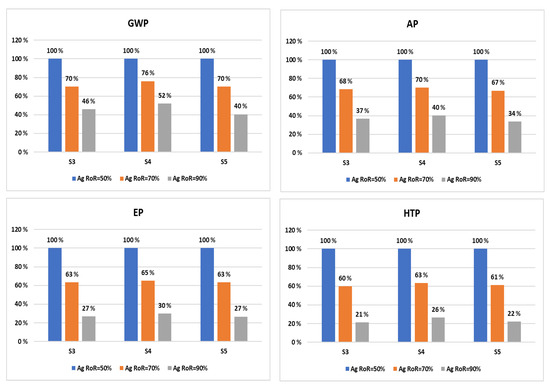
Figure 4.
Sensitivity analysis of silver recycling rate (Ag-RoR).
The recovery rate of silver depends on the silver content in the scrap electronics and recycling practices, which varies in different geographical locations. The Nordic region is considered a high-ranked, affluent part of Europe, due to its high consumption of electronic products per capita [33].
As this analysis illustrates, there would be environmental benefits from the recovery of silver content from electronic waste; however, even in Europe, the lack of recycling facilities hinders the recycling of metal contents of scrap electronics [30]. The aim of this sensitivity analysis was to depict the potential benefits of a higher recycling rate of silver and examine the uncertainty of the results. To conduct a comprehensive environmental study, the impacts of the silver recovery process should be also included.
3.1.2. Sensitivity Analysis of Energy Consumption
Figure 5 demonstrates the sensitivity analysis of the energy consumption in Scenario 1. Regarding energy (electricity and heat) consumption, in S1, as mentioned in the LCI section, the Ecoinvent 3.6 database reported higher values for PCB production. Although, in this study, a conservative value of 20 kWh was adopted for electricity consumption in S1, the environmental impacts of a higher energy consumption are shown in Figure 5.
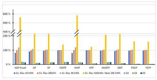
Figure 5.
Sensitivity analysis of energy consumption in scenario 1.
In case the electricity consumption increases by 10%, the GWP of S1 will increase by 25%. The electricity consumption in this scenario causes high uncertainty in the environmental impact assessment of scenarios 1 and 2. As depicted in Figure 5, the reduction in the electricity consumption in S1 to 10 kWh did not result in a lower impact compared to scenarios S3–S5.
3.1.3. Sensitivity Analysis of Ag NP Thickness and Net Area Coverage
The thickness of the ink film on the substrate may vary in different PCB designs to fulfill the electronical requirements of the product. In addition, the net area covered by the silver ink depends on the design parameters of the PCB. Variations in these two parameters affect the mass of the silver ink, and consequently change the mass of silver and the resin consumption in S2–S5. A sensitivity analysis was carried out to determine the effect of variations in Ag NP thickness and net area coverage. Thus, in scenarios S2, S3, S4 and S5, three ink thicknesses of 5, 10 and 15 μm and two values for net area coverage (50% and 80%) were utilized to examine the dependency of four LCI categories of GWP, AP, EP and HTP on the thickness and net area coverage of Ag NP.
Figure 6 shows the sensitivity analysis of the thickness and net area coverage of ink. The environmental impacts of S1 for the inventory listed in Table 2 were selected as the reference for other cases. The baseline in this case represents a thickness of 5 μm and area coverage of 50%. The charts provide data for the five scenarios described in Table 1, and six thickness-covered area combinations for Ag NPs.
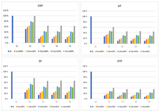
Figure 6.
Sensitivity analysis of Ag NP ink thickness and net area coverage; at the baseline (BL) of S2–S5, the thickness of ink is 5 μm and 50% of the substrate is covered by silver ink.
Regarding the GWP of S2, when the ink layer thickness increases from 5 to 15 μm and the net ink coverage increases from 50% to 80%, the environmental impacts are doubled and the GWP of S2 is the same as that of S1. The variation in environmental impacts in S3, S4 and S5 for the selected impact categories are approximately similar and about four times higher when the thickness of ink changes from 5 to 15 μm and the net ink coverage increases from 50% to 80%. The thickness and area coverage of silver have a direct effect on the mass of Ag NP: a thicker ink or higher area coverage leads to a higher consumption of Ag NP.
4. Conclusions
In this study, we investigated the environmental impacts of the manufacturing of conventional printed circuit boards (PCBs) and the environmental benefits of alternative manufacturing methods. The focus of this study was the utilization of PET, PLA/GF and paper as the PCB substrates and silver nanoparticles as the conductive material. The results of the environmental lifecycle assessment (LCA) showed a significant decline in all the studied environmental impact categories for the scenarios with PET, PLA/GF and paper substrates.
In conventional PCB manufacturing, electricity and chemicals had the highest impacts for GWP and accounted for 41% and 25% of the total impacts. In scenarios 3, 4 and 5, silver nanoparticles had the highest contribution; silver accounted for 83%, 84% and 94% of the GWP in scenarios S3, S4 and S5, respectively.
There is a very large range in the electricity consumption values for S1 in the literature, and so it is a sensitive and uncertain modeling parameter. Our selection for the electricity consumption followed a conservative approach and complied with the lowest reasonable value; however, as shown in the sensitivity analysis section, the conclusions of the study remained the same.
In the PCB manufacturing industry, the transition from subtractive manufacturing to additive manufacturing may significantly decrease the environmental impacts. When using heavy metals such as silver as the conductive material, it is crucial to minimize the material consumption to diminish the environmental impacts of PCB production. On the other hand, a higher recycling rate of metals in the EoL stage could reduce the total environmental impacts.
Author Contributions
Conceptualization, M.N.N. and I.D.; methodology, M.N.N.; software, M.N.N.; validation, I.D., M.H.; investigation, M.N.N.; writing—original draft preparation, M.N.N.; writing—review and editing, I.D. and M.H.; visualization, M.N.N.; supervision, I.D. and M.H.; project administration, I.D., M.H. and V.L.; funding acquisition, V.L. All authors have read and agreed to the published version of the manuscript.
Funding
The authors would like to acknowledge the Business Finland’s ECOtronics project for their funding, under the project number 2156/31/2019.
Acknowledgments
The authors would like to thank the other researchers in the ECOtronics project (Liisa Hakola, Mika Suhonen and Kirsi Immonen) for providing technical insights regarding the selection of materials and manufacturing processes.
Conflicts of Interest
The authors declare no conflict of interest.
References
- Sullivan, M.; Sensors for the Internet of Things (IOT): Global Markets. BCC Research. 2017. Available online: https://www.bccresearch.com/market-research/information-technology/sensors-for-the-internet-of-things-iot-global-markets.html (accessed on 20 January 2021).
- Kosbar, L.L.; Gelorme, J.D.; Japp, R.M.; Fotorny, W.T. Introducing Biobased Materials into the Electronics Industry. J. Ind. Ecol. 2000, 4, 93–105. [Google Scholar] [CrossRef]
- Clyde, J.; Coombs, F. Printed Circuits Handbook, 6th ed.; McGraw-Hill Education: New York, NY, USA, 2008; Available online: https://www.accessengineeringlibrary.com/content/book/9780071467346 (accessed on 15 January 2021).
- Deng, Y.; Van Acker, K.; Dewulf, W.; Duflou, J. Environmental Assessment of Printed Circuit Boards from Biobased Materials. In Glocalized Solutions for Sustainability in Manufacturing; Springer: Berlin/Heidelberg, Germany, 2011; pp. 605–610. [Google Scholar]
- Deng, Y.; Paraskevas, D.; Tian, Y.; Van Acker, K.; Dewulf, W.; Duflou, J.R. Life cycle assessment of flax-fibre reinforced epoxidized linseed oil composite with a flame retardant for electronic applications. J. Clean. Prod. 2016, 133, 427–438. [Google Scholar] [CrossRef]
- Liu, J.; Yang, C.; Wu, H.; Lin, Z.; Zhang, Z.; Wang, R.; Li, B.; Kang, F.; Shi, L.; Wong, C.P. Future paper based printed circuit boards for green electronics: Fabrication and life cycle assessment. Energy Environ. Sci. 2014, 7, 3674–3682. [Google Scholar] [CrossRef]
- Mattana, G.; Briand, D.; Marette, A.; Quintero, A.V.; de Rooij, N.F. Polylactic acid as a biodegradable material for all-solution-processed organic electronic devices. Org. Electron. 2015, 17, 77–86. [Google Scholar] [CrossRef]
- Huttunen, A.; Kurkela, T.; Vaisanen, K.-L.; Juntunen, E. Multilayer plastic substrate for electronics. In Proceedings of the 2018 7th Electronic System-Integration Technology Conference (ESTC), Dresden, Germany, 18–21 September 2018. [Google Scholar] [CrossRef]
- Drumright, R.E.; Gruber, P.R.; Henton, D.E. Polylactic acid technology. Adv. Mater. 2000, 12, 1841–1846. [Google Scholar] [CrossRef]
- Lim, L.-T.; Auras, R.; Rubino, M. Processing technologies for poly(lactic acid). Prog. Polym. Sci. 2008, 33, 820–852. [Google Scholar] [CrossRef]
- Siracusa, V.; Blanco, I.; Romani, S.; Tylewicz, U.; Rocculi, P.; Rosa, M.D. Poly(lactic acid)-modified films for food packaging application: Physical, mechanical, and barrier behavior. J. Appl. Polym. Sci. 2012, 125, E390–E401. [Google Scholar] [CrossRef]
- Saeidlou, S.; Huneault, M.A.; Li, H.; Park, C.B. Poly(lactic acid) crystallization. Prog. Polym. Sci. 2012, 37, 1657–1677. [Google Scholar] [CrossRef]
- Martin, O.; Avérous, L. Poly(lactic acid): Plasticization and properties of biodegradable multiphase systems. Polymer 2001, 42, 6209–6219. [Google Scholar] [CrossRef]
- Rasal, R.M.; Janorkar, A.V.; Hirt, D.E. Poly(lactic acid) modifications. Prog. Polym. Sci. 2010, 35, 338–356. [Google Scholar] [CrossRef]
- Wang, G.; Zhang, D.; Wan, G.; Li, B.; Zhao, G. Glass fiber reinforced PLA composite with enhanced mechanical properties, thermal behavior, and foaming ability. Polymer 2019, 181, 121803. [Google Scholar] [CrossRef]
- Karger-Kocsis, J.; Mahmood, H.; Pegoretti, A. Recent advances in fiber/matrix interphase engineering for polymer composites. In Progress in Materials Science; Elsevier Ltd.: Amsterdam, The Netherlands, 2015; Volume 73, pp. 1–43. [Google Scholar] [CrossRef]
- Chen, S.; Liu, K.; Luo, Y.; Jia, D.; Gao, H.; Hu, G.; Liu, L. In situ preparation and sintering of silver nanoparticles for low-cost and highly reliable conductive adhesive. Int. J. Adhes. Adhes. 2013, 45, 138–143. [Google Scholar] [CrossRef]
- Liu, Z.; Ji, H.; Wang, S.; Zhao, W.; Huang, Y.; Feng, H.; Wei, J.; Li, M. Enhanced Electrical and Mechanical Properties of a Printed Bimodal Silver Nanoparticle Ink for Flexible Electronics. Phys. Status Solidi Appl. Mater. Sci. 2018, 215, 1–9. [Google Scholar] [CrossRef]
- Yang, M.; Chon, M.-W.; Kim, J.-H.; Lee, S.-H.; Jo, J.; Yeo, J.; Ko, S.H.; Choa, S.-H. Mechanical and environmental durability of roll-to-roll printed silver nanoparticle film using a rapid laser annealing process for flexible electronics. Microelectron. Reliab. 2014, 54, 2871–2880. [Google Scholar] [CrossRef]
- Jang, S.; Rahman, M. Effect of sintering atmospheres on printed silver nanoparticle patterns for flexible electronics application. Appl. Phys. A 2021, 127, 1–14. [Google Scholar] [CrossRef]
- Barmpakos, D.; Tsamis, C.; Kaltsas, G. Multi-parameter paper sensor fabricated by inkjet-printed silver nanoparticle ink and PEDOT:PSS. Microelectron. Eng. 2020, 225, 111266. [Google Scholar] [CrossRef]
- Rubin, R.S.; Castro, M.; Brandão, D.; Schalch, V.; Ometto, A.R. Utilization of Life Cycle Assessment methodology to compare two strategies for recovery of copper from printed circuit board scrap. J. Clean. Prod. 2014, 64, 297–305. [Google Scholar] [CrossRef]
- ISO. 14040: Environmental Management–Life Cycle Assessment—Principles and Framework; International Organization for Standardization: Geneva, Switzerland, 2006. [Google Scholar]
- Hischier, R.; Classen, M.; Lehmann, M.; Scharnhorst, W. Swiss Centre for Life Cycle inventories (Ecoinvent v2.0): Part ll: Modules; Ecoinvent v2.0; Swiss Centre for Life Cycle Inventories: Zurich, Switzerland, 2007; p. 116. [Google Scholar]
- Ozkan, E.; Elginoz, N.; Babuna, F.G. Life cycle assessment of a printed circuit board manufacturing plant in Turkey. Environ. Sci. Pollut. Res. 2017, 25, 26801–26808. [Google Scholar] [CrossRef]
- Bogdanski, G.; Schönemann, M.; Thiede, S.; Andrew, S.; Herrmann, C. An extended energy value stream approach applied on the electronics industry. In IFIP Advances in Information and Communication Technology; Springer: Berlin/Heidelberg, Germany, 2013; Volume 397, pp. 65–72. [Google Scholar] [CrossRef] [Green Version]
- Schweitzer, A. Cost Drivers in Manufacturing of PCBs. 2017. Available online: https://www.flowcad.ch/cms/upload/downloads/PCBRoadshow2017CostDriver.pdf (accessed on 20 January 2021).
- Multi Circuit Boards Ltd. Defined Layer Buildup of Multi Layer PCB. 2021. Available online: https://www.multi-circuit-boards.eu/en/pcb-design-aid/layer-buildup/standard-buildup.html (accessed on 10 January 2021).
- Xue, M.; Kendall, A.; Xu, Z.; Schoenung, J. Waste Management of Printed Wiring Boards: A Life Cycle Assessment of the Metals Recycling Chain from Liberation through Refining. Environ. Sci. Technol. 2015, 49, 940–947. [Google Scholar] [CrossRef] [PubMed]
- Bakas, I.; Herczeg, M.; Vea, E.B.; Fråne, A.; Youhanan, L.; Baxter, J. Critical Metals in Discarded Electronics, Mapping Recycling Potentials from Selected Waste Electronics in the Nordic Region; Nordisk Ministerråd: Copenhagen, Denmark, 2016. [Google Scholar]
- Temizel-Sekeryan, S.; Hicks, A.L. Global environmental impacts of silver nanoparticle production methods supported by life cycle assessment. Resour. Conserv. Recycl. 2020, 156, 104676. [Google Scholar] [CrossRef]
- Pourzahedi, L.; Eckelman, M.J. Comparative life cycle assessment of silver nanoparticle synthesis routes. Environ. Sci. Nano 2015, 2, 361–369. [Google Scholar] [CrossRef]
- Eurostat. Waste Statistics—Electrical and Electronic Equipment—Statistics Explained; Eurostat Statistics Explained: Luxembourg, 2017. [Google Scholar]
Publisher’s Note: MDPI stays neutral with regard to jurisdictional claims in published maps and institutional affiliations. |
© 2021 by the authors. Licensee MDPI, Basel, Switzerland. This article is an open access article distributed under the terms and conditions of the Creative Commons Attribution (CC BY) license (https://creativecommons.org/licenses/by/4.0/).