Article

Parallel Power Sharing Control of Multi-Controllable Rectifiers in a High-Power DC Fast Charging Station

1
School of Electrical Engineering, Tiangong University, Tianjin 300387, China
2
School of Control Science and Engineering, Tiangong University, Tianjin 300387, China
*
Authors to whom correspondence should be addressed.
World Electr. Veh. J. 2023, 14(7), 193; https://doi.org/10.3390/wevj14070193
Submission received: 25 June 2023 / Revised: 13 July 2023 / Accepted: 14 July 2023 / Published: 21 July 2023

Abstract

:
The increase in demand for the fast charging of electric vehicles (EVs) has promoted research and the application of high-power direct current (DC) fast charging stations, and research on the stability control of charging stations with a parallel structure of multi-controllable rectifier modules is of great significance. Taking into account the dynamic and steady-state performance, the parameters of the dual-loop controller based on virtual impedance control are designed to realize the power sharing of multi-controllable rectifier modules. The constant power load model of EV charging at a constant current is established, and the load capacity of the cascaded system of converters is studied by using the impedance analysis method. The experimental and simulation results verify the effectiveness and correctness of the power sharing control strategy and the cascaded system stability analysis.

1. Introduction

In recent years, various fields of social development have been striving for zero-carbon emission energy transformation. As a new type of transportation, EVs, which have the advantages of zero emissions, high reliability, low maintenance cost, and easy access to renewable energy and energy storage systems, are attracting more and more consumers. Ensuring a good control effect of the EV charging station system and providing safe, efficient, and stable charging services for car owners is a key measure to promote the development of the EV industry. With the continuous improvement in people’s requirements for the EV charging time, DC fast charging stations have been widely researched and applied due to the advantages of fewer conversion levels, easy connection with distributed power sources, and high efficiency.
A typical DC fast charging station topology is shown in Figure 1, which includes a DC–DC converter, an AC–DC converter, and a filter. AC–DC conversion is the first stage in EV fast charging. The AC–DC converter rectifies the AC voltage of the grid into DC voltage, and it is usually designed as a three-phase half-bridge [1]. DC–DC conversion is the second stage to control the input voltage to the EV battery. Common DC–DC converter topologies include interleaved and multi-stage non-isolated, and isolated half-bridge, full-bridge, Z-source, and flyback [2,3]. The filter can guarantee lower total harmonic distortion (THD) of the grid side current. The AC–DC converter controls the stability of the DC bus voltage, and the DC–DC converter can match the charging voltage of different types of EVs.
Current research on DC fast charging stations focuses on topology design and improving control performance. Reference [4] proposed a bidirectional five-level step-down converter, which uses two voltage sensors with complex control strategies to balance the voltage across two capacitors, but will lead to input current distortion and THD increase under light load conditions. Reference [5] proposed an improved three-phase step-down converter to reduce the influence of distributed parasitic capacitance between the DC bus and the system ground. The Swiss rectifier is a step-down power factor correction (PFC) converter topology suitable for EV charging systems with 250–450 V DC bus voltage and 380 V three-phase AC voltage [6]. Swiss rectifiers have low common-mode noise and low switching losses in complex power circuits [7,8]. Compared with the three-level rectifier, the Vienna rectifier, which has been widely used in recent years, has many advantages, such as a high power density, fewer switches, lower THD, and no neutral point connection structure [9,10]. Conventional control methods for Vienna rectifiers include sliding mode control, hysteresis current control, and double closed-loop control, which can adjust the DC bus voltage and unit power factor. Dual active bridge (DAB) converters in isolated DC–DC converters are often used in EV fast charging systems due to their advantages of high efficiency, high reliability, bidirectional power flow, and low filter requirements. Scholars have studied DAB converters using various types of resonant tanks, such as LC, LCL, CLC, LLL, and CLLC [11,12,13]. Reference [14] adopts an improved modulation technique to extend the zero voltage switching (ZVS) range of EV battery charging. Because the EV battery voltage is usually lower than the input voltage of the DC–DC converter, non-isolated BUCK converters are also commonly used in EV fast charging systems. Reference [15] analyzed the charge and discharge loss caused by the current ripple of the BUCK converter and proved the importance of applying the multi-inductance interleaved BUCK converter to the EV fast charging system.
EV charging stations with scattered installation locations are connected to the grid through transmission cables of different lengths. The resonance of parasitic inductance and capacitance on the transmission cables will amplify the background harmonics. Reference [16] proposes a harmonic resonance suppression strategy for Vienna rectifiers to improve the power quality of the grid current and at the point of the public coupling voltage. Reference [17] proposes an improved dead-beat control method, using active disturbance rejection control in the voltage loop, and introducing the AC side voltage compensation coefficient in the current loop to improve the dynamic performance of the system. Reference [18] studied the coupling mechanism between the DC bus voltage ripple and the grid harmonic current under the condition of an unbalanced grid voltage, and proposes that the grid current harmonics can be reduced by an improved proportional quasi-resonant (IPQR) controller.
In terms of power sharing controls for charging stations, reference [19] proposes the interval type2 fuzzy logic controller-based power-sharing strategy to utilize hybrid energy storages in the solar-powered charging station effectively. The hybrid energy storage system consists of a battery and supercapacitor with solar power generation as a primary source. The battery supports the slow varying power, and the supercapacitor supports the fast varying power. Reference [20] proposes a distributed online algorithm to promote energy sharing between charging stations from the perspective of reducing the operating cost of the charging stations. The goal is to minimize the long run time-averaged total cost. The proposed algorithm can preserve privacy while being suitable for online implementation. Different optimization algorithms are applied in the power sharing control of charging stations to solve the optimization problem per concerns regarding data privacy, individual economic interests, and EV uncertainties [21,22].
In addition, some scholars have focused on the interactive control of the EV charging system and power grid. Reference [23] studied the influence of grid voltage disturbance on the EV charging system composed of a three-phase controllable rectifier and DC–DC converter. Reference [24] presents an adaptive notch filter-based efficient control algorithm for a multifunctional grid connected solar photovoltaic powered EV charger to power the EV batteries and simultaneously improve the grid power quality. Reference [25] proposes a hierarchical economic model predictive control scheme to achieve intelligent and coordinated charging management of EVs. A decentralized EV charging control system has proven that the EV can adjust the charging power according to the voltage level of the low-voltage distribution network to reduce the investment cost of the distribution network [26]. Reference [27] proposes a simplified small signal model for the LLC resonant converter, which greatly simplifies the design of the underlying controller.
At present, there is little research on the control of EV high-power DC fast charging stations, especially the DC fast charging station with multiple controllable rectifier modules in parallel. It is a key issue to ensure that the system is stable and ensure power sharing of the multiple modules. This paper conducts research on the controller design of an EV high-power DC fast charging station, and the main contributions are as follows:
(1)
The power sharing controller parameters based on virtual impedance control are designed, including the current loop, voltage loop proportional integral (PI) controller parameters, and virtual impedance parameters. Considering the bandwidth and stability of the current loop and voltage loop, the parameters of the PI controller are designed. According to the principle of shielding the natural output impedance of the system and ensuring the fluctuation range of the DC bus voltage, the virtual impedance is designed to realize the stability of the DC bus voltage and the power sharing of multiple controllable rectifier modules.
(2)
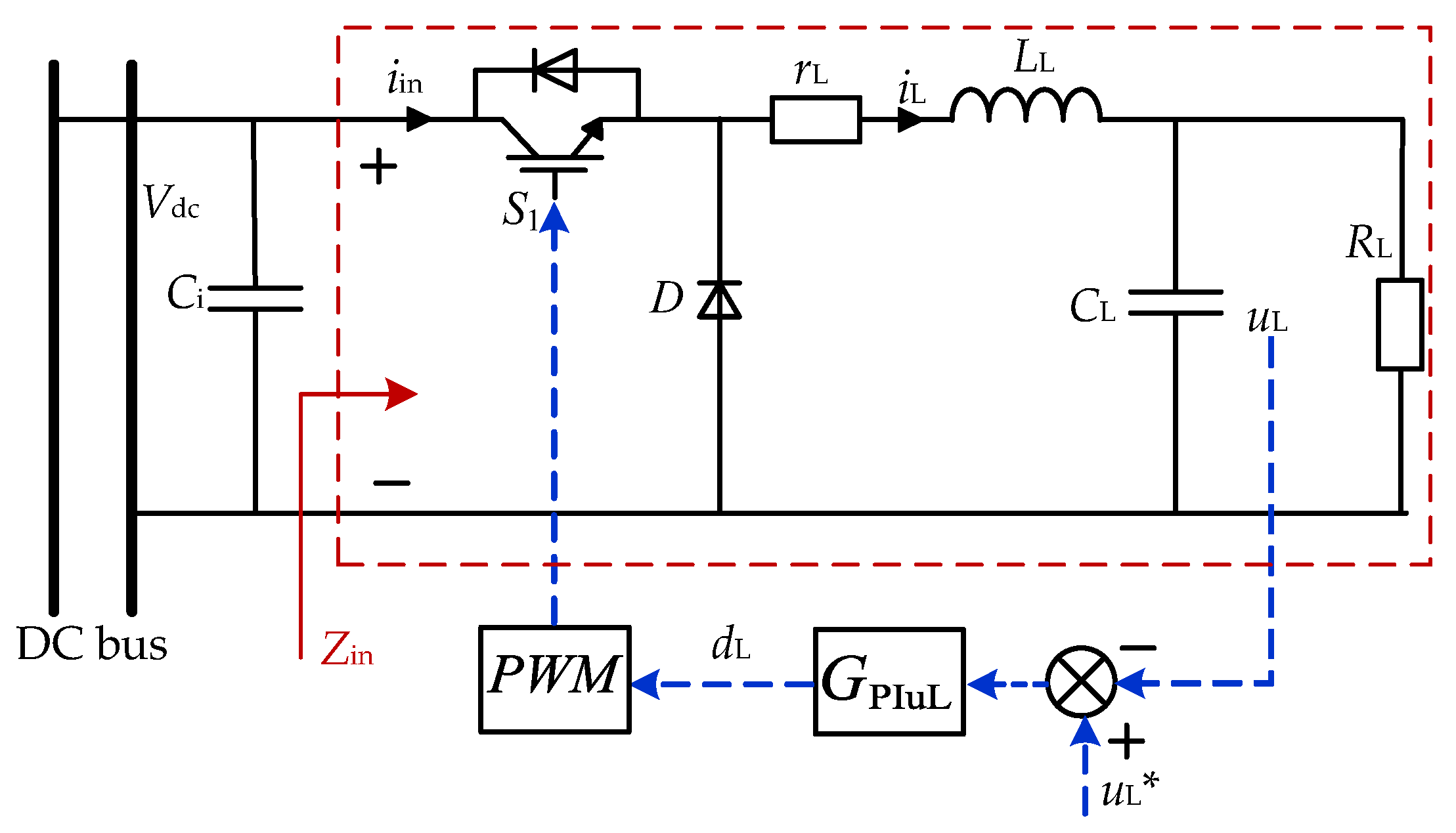
Considering that an EV can be equivalent to a constant power load when it is charged with a constant current, a constant voltage-controlled Buck converter with a resistive load is used to simulate the constant power load, and a mathematical model of its input impedance is established. Using the impedance analysis method, the cascaded system composed of multiple parallel controllable rectifier modules and a DC–DC converter is used to study the maximum load that can be tolerated when EV is charged with a constant current.

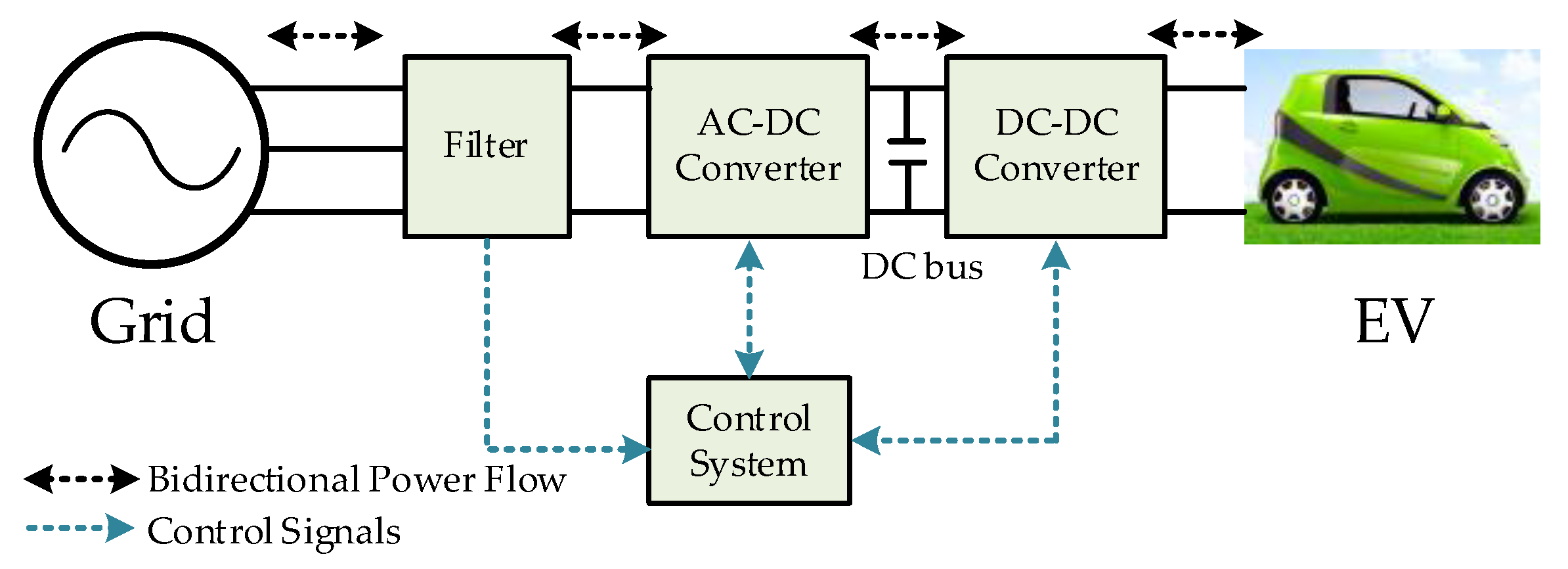
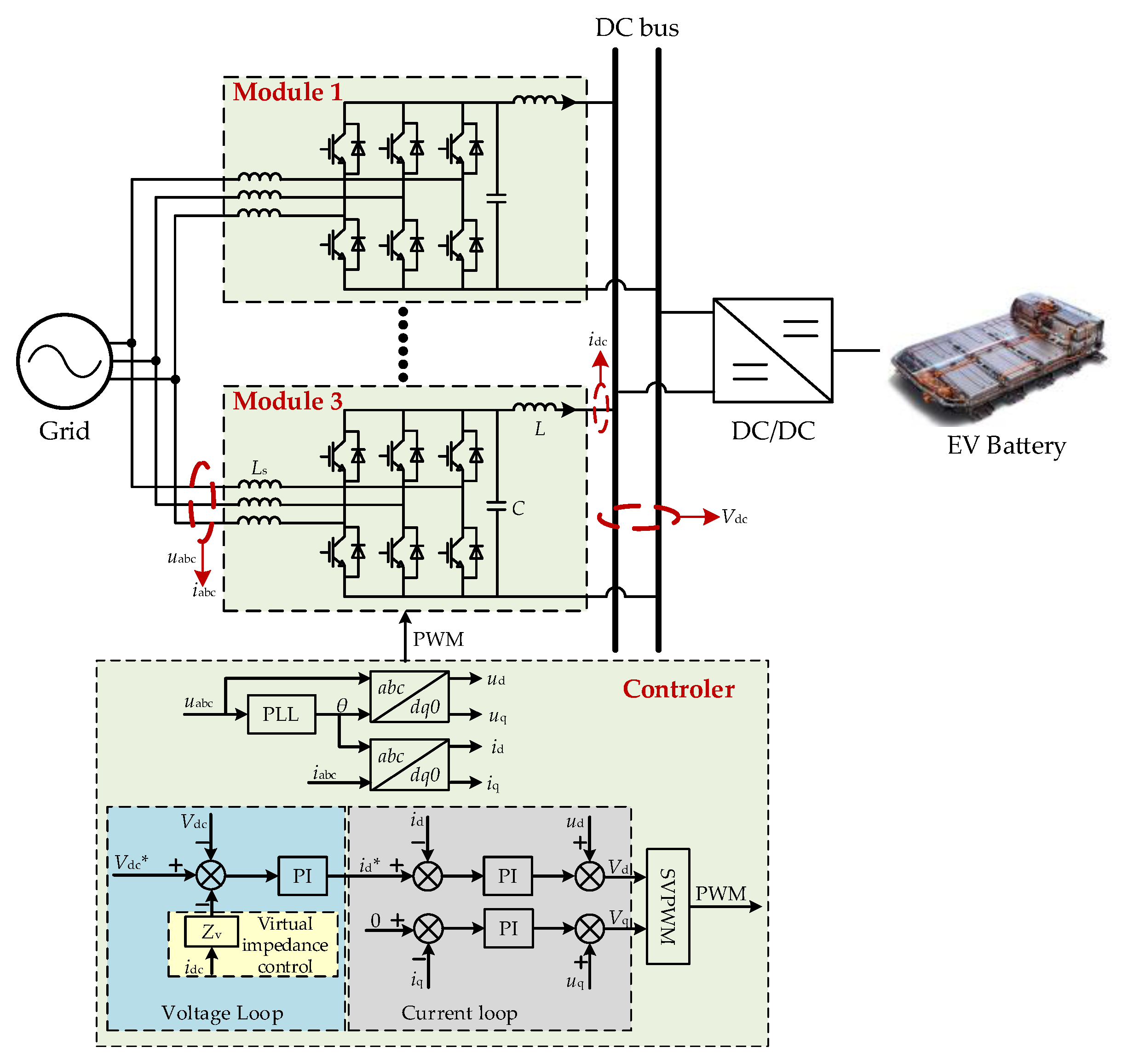
2. High-Power DC Fast Charging Station Topology and Controller Structure

The topology and controller structure of the high-power DC fast charging station studied in this paper are shown in Figure 2. Three controllable rectifier modules with a rated capacity of 60 kW are connected in parallel to the same AC bus through the filter inductor Ls. The modules adopt a three-phase half-bridge topology, and their DC sides are connected in parallel to the same DC bus through the inductor L that suppresses the impact of the parallel current. The DC–DC converter connected to the DC bus is connected to the EV battery, and the output voltage of the DC–DC converter can be controlled to adapt to the charging voltage of different types of EV batteries, providing fast charging with a maximum power of 180 kW.
The key to the stable operation of high-power DC fast charging stations is the stable control of the DC bus voltage. Each controllable rectifier module is controlled separately, and the signals to be collected include the DC bus voltage, Vdc, the outlet current, idc, of each module, and the grid-side voltage, uabc, and current, iabc. The controller of each module adopts a double-loop structure. The inner loop is the current loop, and the iabc is converted to the d–q coordinate system and is controlled by the PI controller. The q-axis controller is ignored because the system is at a unity power factor (i.e., the current reactive component reference value iq* = 0), and the voltage active power control is mainly affected by the d-axis active current. The outer loop is a voltage loop based on virtual impedance control, Zv is the virtual impedence and Vdc* is the reference value of the DC bus voltage. The output of the voltage loop PI controller is id*, the reference value of the d-axis component, id, of the current loop. Power sharing between different modules can be realized by designing the virtual impedance, Zv. The main circuit and controller transfer function model of each rectifier module are shown in Figure 3.

3. Parameter Design of the Power Sharing Controller
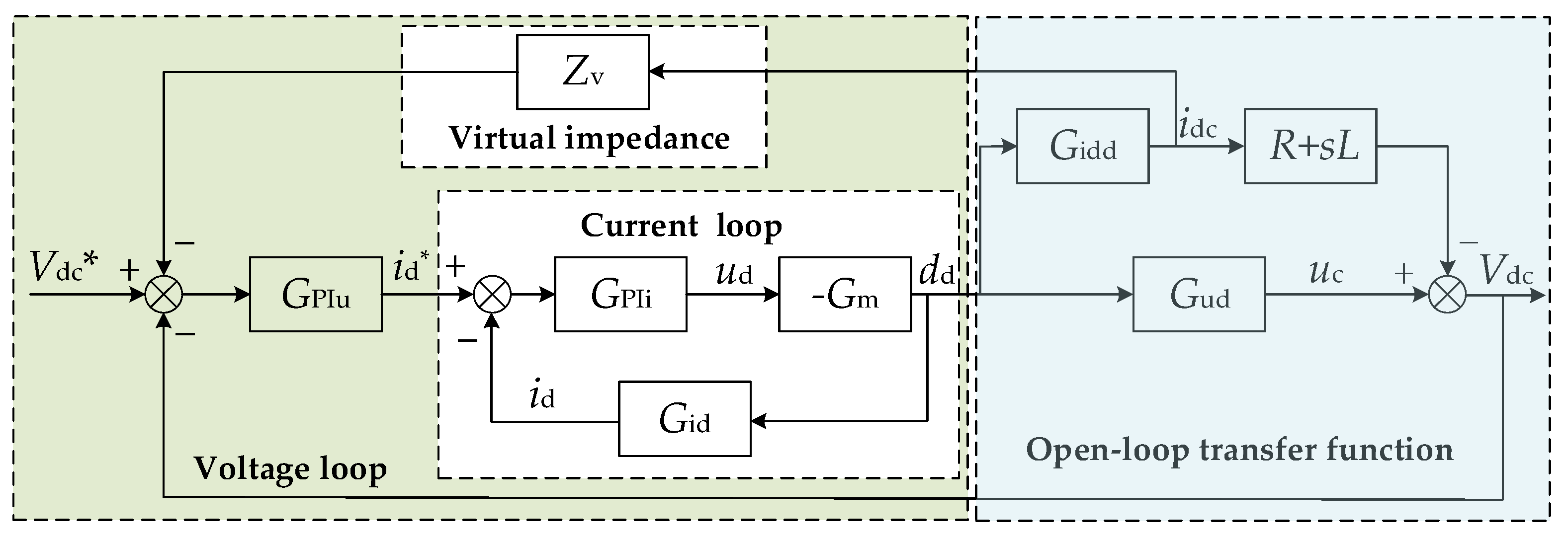
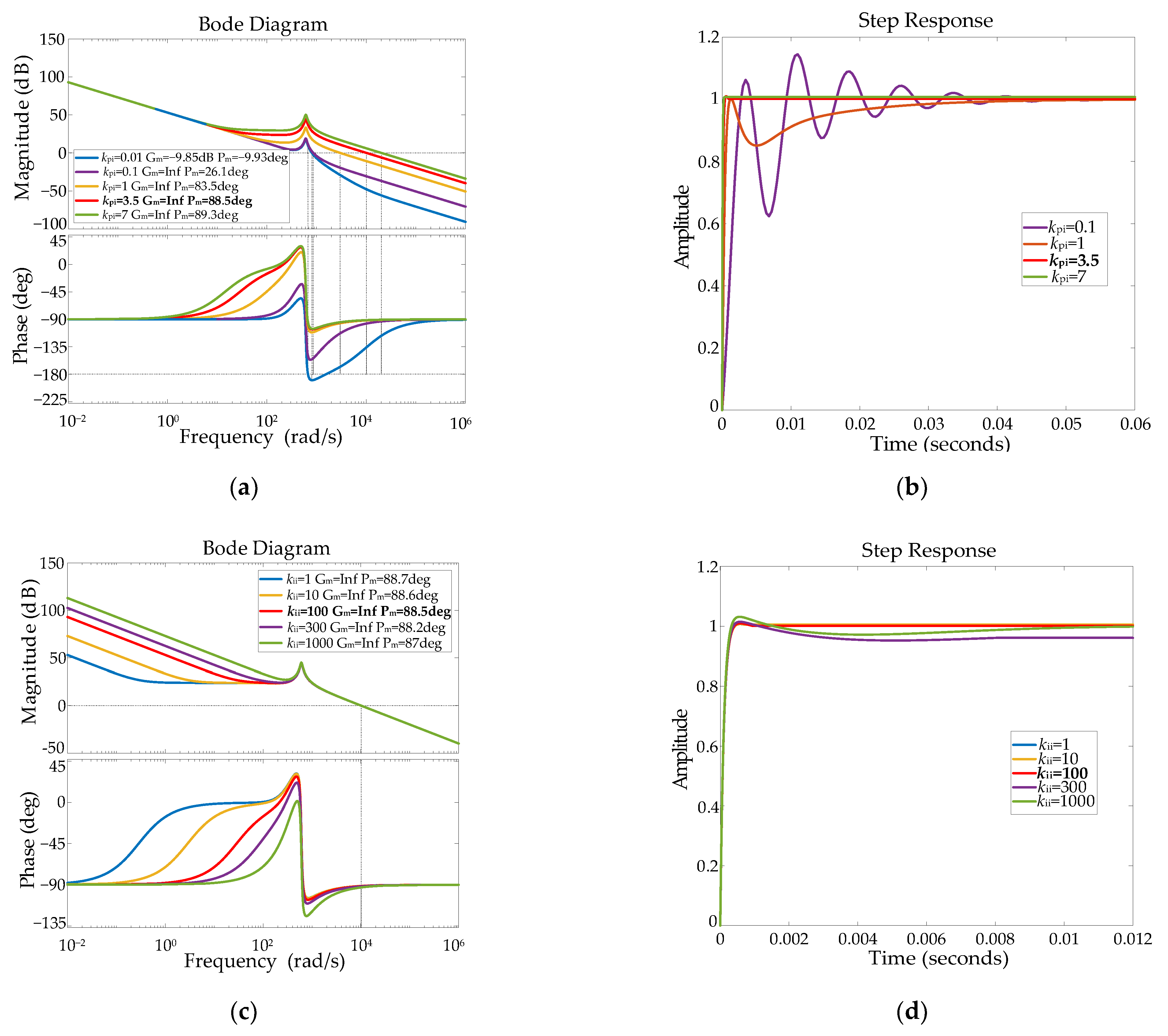
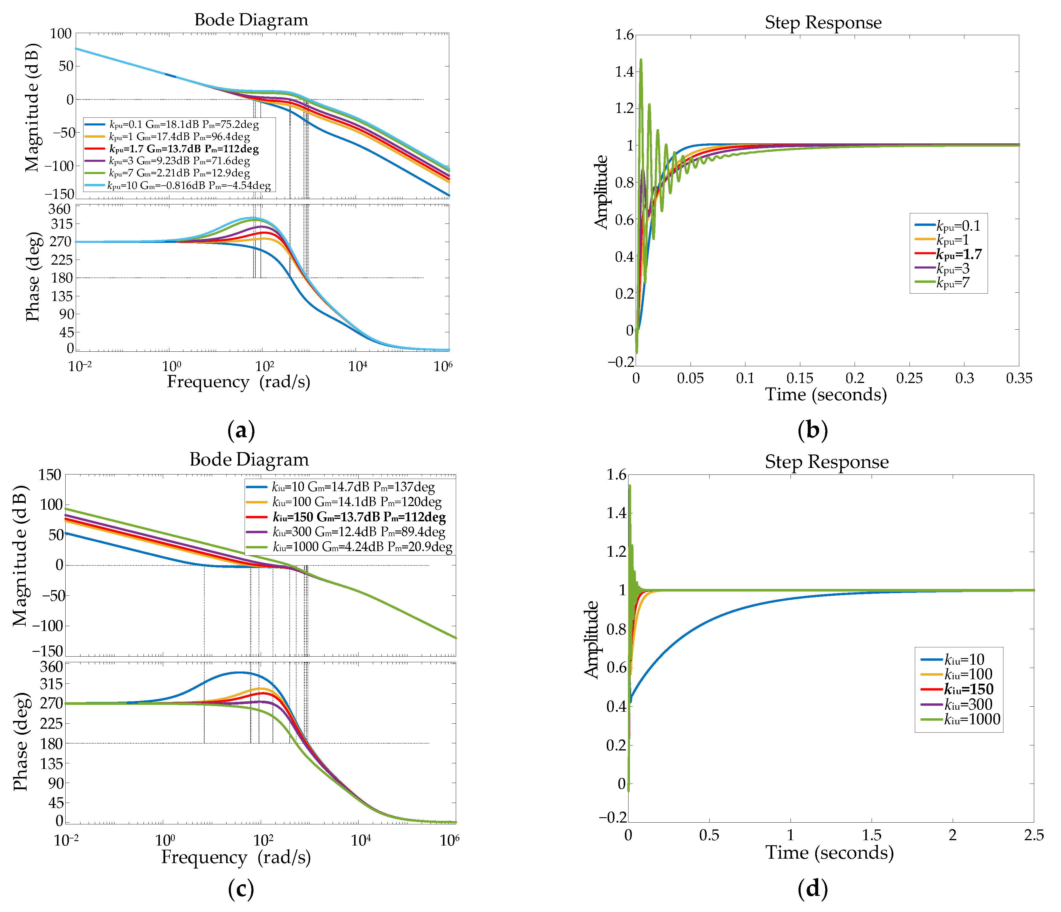
3.1. Current Loop

From Figure 3, Gm is the transfer function of the SVPWM modulation module; Gid is the transfer function from the duty cycle, dd, to the d-axis component of the AC side current, id; Gidd is the transfer function from the duty cycle, dd, to the output current, idc; and Gud is the transfer function from the duty cycle, dd, to the DC side capacitor voltage, uc; GPii is the PI controller in the inner current loop; GPiu is the PI controller in the outer voltage loop. The transfer functions of Gm, Gid, Gud, and Gidd can be expressed as:
G m = 3 2 V dc
G id = i ^ d d ^ d = C L U c s 2 + 1.5 I d D d L + U c C L L s s 3 + C L s R L s 2 + 1.5 D d 2 L + L s s + 1.5 D d 2 R L
G idd = i ^ dc d ^ d = 1.5 D d U c 1.5 I d L s s 1.5 I d R s C L L s s 3 + C L s R L s 2 + 1.5 D d 2 L + L s s + 1.5 D d 2 R L
G ud = u ^ c d ^ d = 1.5 I d L L s s 2 + ( 1.5 D d U c L 1.5 I d R L L s ) s + 1.5 D d U c R L C L L s s 3 + C L s R L s 2 + ( 1.5 D d 2 L + L s ) s + 1.5 D d 2 R L
where the superscript ‘^’ indicates the small signal perturbation; dd is the d-axis component of the duty cycle; id is the d axis components of the AC side inductor current; uc is the DC side capacitor voltage; idc is the output current of the DC side; ud is the d axis components of uabc; id* is the inner current reference value; Dd, Id, and Uc are the corresponding steady-state operating points; Ls is the AC side inductance; Rs is the equivalent resistance of the AC side; C is the DC side capacitor; L is the paralleled inductance; RL is the load resistance; Vdc is the DC bus voltage; Zv is the virtual impedance.
The open-loop transfer function Gio in the current loop controller from id* to id can be expressed as:
G io = G PIi G m G id
The closed-loop transfer function Gio in the current loop controller from igd* to igd can be expressed as:
G ic = G PIi G m G id 1 + G PIi G m G id
The open-loop frequency response and closed-loop step response in the current loop vary with the proportional coefficient kpi and integral coefficient kii of the PI controller, as shown in Figure 4 and Table 1. With the increase in kpi, the response speed of the current loop becomes faster, the overshoot of the system decreases, the phase angle margin becomes larger, and the stability becomes better. With the increase in kii, the response speed of the current loop becomes faster, the overshoot increases, and the phase angle margin decreases slightly. Considering the dynamic performance and steady-state performance of the current loop, the final choice is kpi = 3.5, kii = 100. When kpi = 3.5 and kii = 100, the frequency bandwidth of the current loop is 2.28 kHz, and the phase angle margin is 88.5 deg, while the response time is 0.0006 s, the overshoot σ% = 0, and the steady-state error is 0.0015.

3.2. Voltage Loop

The open-loop transfer function Guo in the voltage loop controller from Vdc* to Vdc can be expressed as:
G uo = G PIu G ic G ud G idd R + s L
The closed-loop transfer function Guc in the voltage loop controller from Vdc* to Vdc can be expressed as:
G uc = G PIu G ic G ud G idd R + s L 1 + G PIu G ic G ud G idd R + s L
The open-loop frequency response and closed-loop step response in the voltage loop vary with the proportional coefficient kpu and integral coefficient kiu in the PI controller, as shown in Figure 5 and Table 2. Within a certain range, with the increase of kpu, the response speed of the voltage loop becomes faster, and the phase angle margin first increases and then decreases. As kiu increases, the response speed of the voltage loop becomes faster, the phase angle margin decreases slightly, and the overshoot increases. Considering the dynamic performance and steady-state performance of the current loop, the final choice is kpu = 1.7 and kiu = 150. When kpu = 1.7 and kiu = 150, the bandwidth in the voltage loop is 42.68 Hz, the phase margin is 112 deg, and the gain margin is 13.7 dB, while the response time is 0.14 s, the system has no overshoot, and the steady-state error is 0.001.

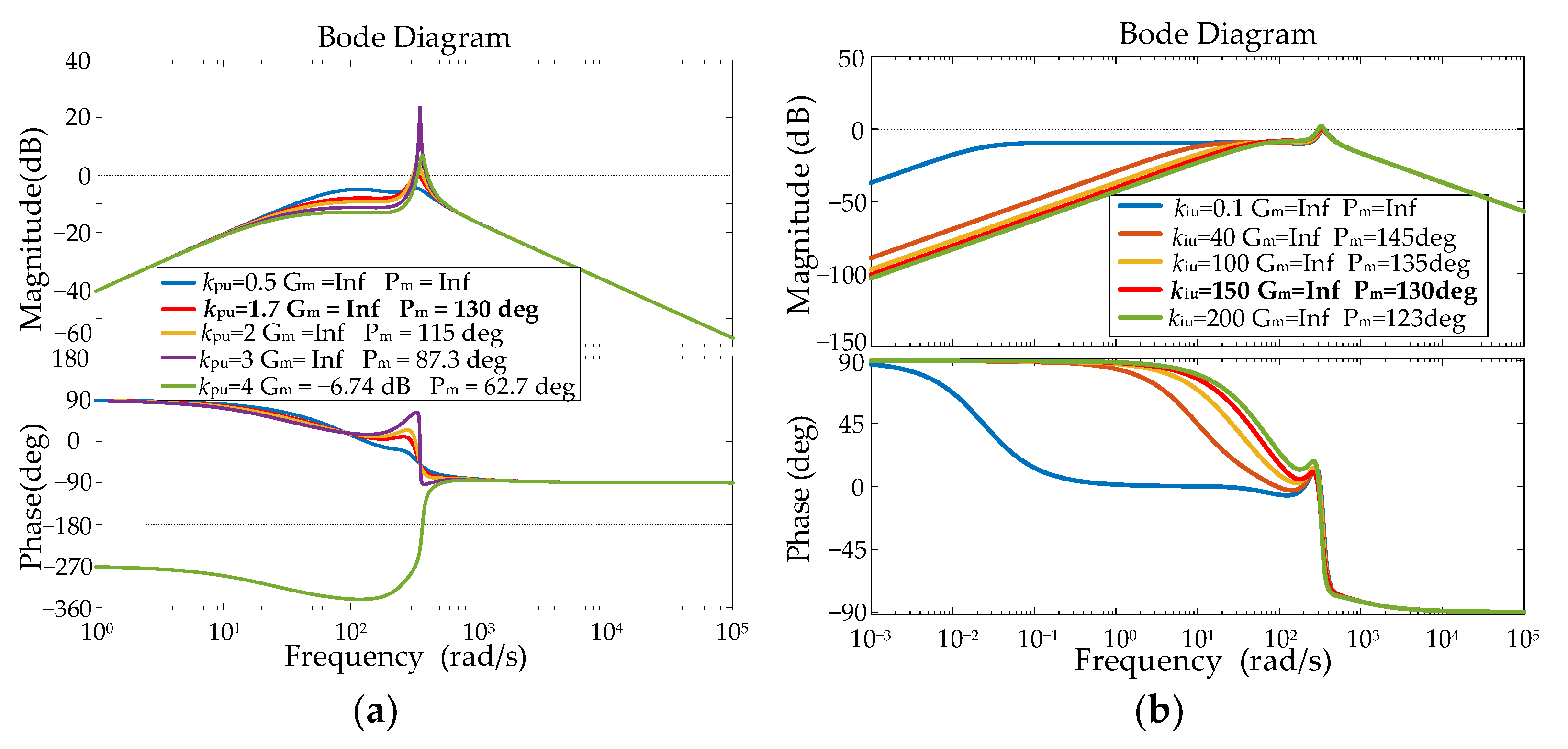
3.3. Virtual Impedance

The natural output impedance transfer function Zno from idc to Vdc can be expressed as:
Z no = G idd ( R + s L ) G ud G idd ( R + s L ) C L s G ud C L s + G idd + G idd G PIu G ic G ud
The impact of the voltage controller parameters on the output impedance Zno is shown in Figure 6. As kpu increases, the gain margin of Zno will decrease and the system will become unstable. Zno is inductive in the low-frequency band and capacitive in the high-frequency band. It can be seen from Figure 6b that kiu has little effect on system stability.
The introduction of virtual impedance in the voltage closed-loop control can reduce the sensitivity of the system’s natural output impedance to the controller parameters. The virtual impedance design should meet the following three principles:
(1)
The virtual impedance Zv must be greater than the natural output impedance Zno to reduce the influence of natural impedance on the power sharing amongst different modules;
(2)
The droop in the DC bus voltage after adding the virtual impedance cannot exceed 5% of the rated voltage when the load power changes from 30% rated power to full-load;
(3)
It is necessary to consider the load capacity of the system. If the virtual impedance is designed to be too large, it will increase the output impedance of the source and reduce the overall load capacity of the system.
According to the above principles, the rated voltage Vdc is selected as 750 V. When the load power is at 30% of the total load, the bus voltage rise should be less than 5%. Similarly, when the load power is at the rated value, the bus voltage should drop by less than 5%. According to Figure 6a, the virtual impedance Zv can be determined by:
Z V = U 1 U 2 I 1 I 2
The output impedance Zov of the system after adding the virtual impedance is as follows:
Z ov = ( 1 + G PIu G ic G idd Z v ) ( G idd R + G idd L s G ud ) ( 1 + G PIu G ic G idd Z v ) ( G idd R C L s + G idd L C L s 2 G ud C L s + G idd ) + G idd G PIu G ic G ud
The frequency–domain response of the transfer function Zov after adding the virtual impedance is shown in Figure 7b. Zov is purely resistive in the low-frequency band. The magnitude of Zov is dominated by its droop coefficient such that the effect of the natural impedance, Zno, in the low-frequency band can be basically ignored. Therefore, considering the above design principles of Zv, this article sets the virtual impedance Zv of each 60 kW module to be 0.2 Ω.

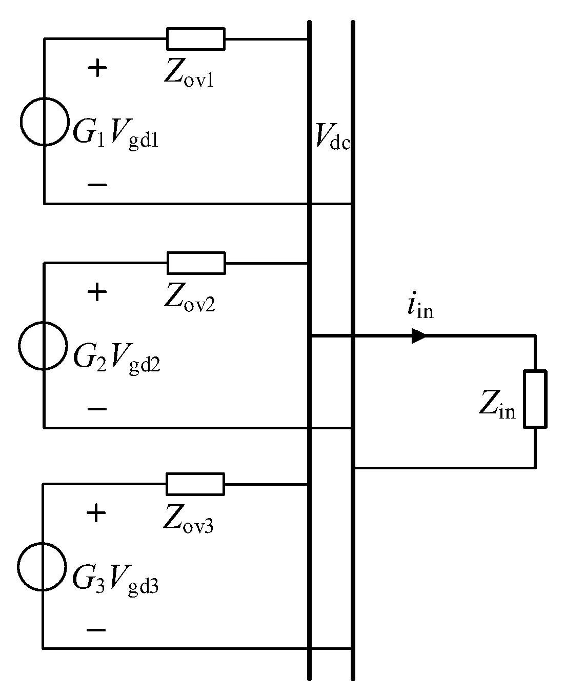
4. Analysis of the Load Capacity of the Cascaded System

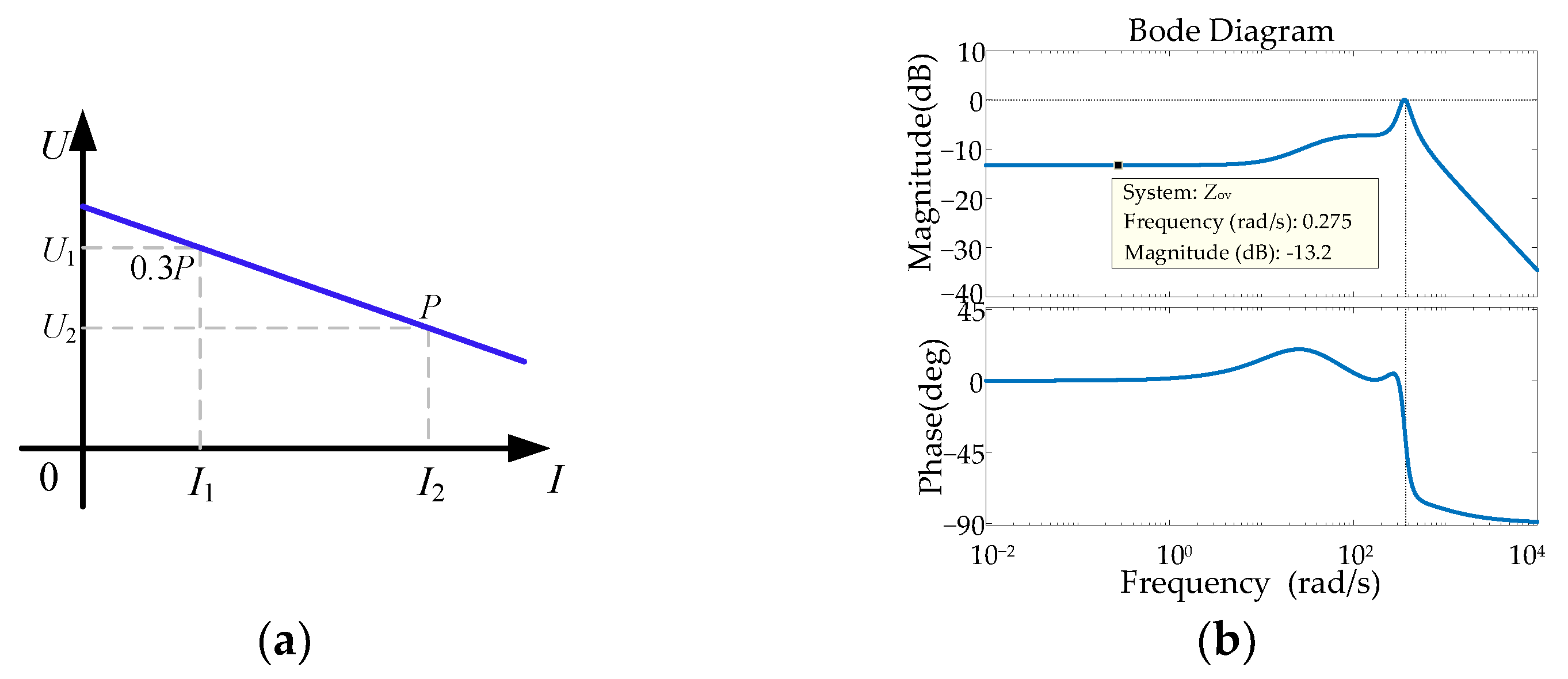
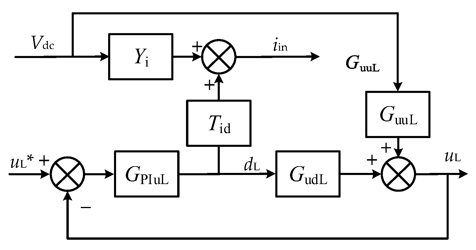
4.1. Input Impedance of a Constant Power Load

When fast charging, EV batteries experience thermal limits and fluctuations, causing fluctuations in the current. The dynamic responses in this paper will occur before the battery experiences thermal limitations and current fluctuations. EV generally uses the method of “constant current first, then constant voltage” for level 1 and level 2 charging. When a DC bus supplies multiple level 2 chargers at once, they are only charging the vehicles from approximately 15% to 80% SOC at level 2, the constant current charging time is relatively long, and the EV battery terminal voltage changes very little during this period, so the EV charging load can be regarded as a constant power load. In this paper, a constant voltage-controlled Buck converter connected to the DC bus with a resistive load is used to simulate the constant power load. The topology and controller structure of the Buck converter are shown in Figure 8.
The state equation of the Buck converter can be expressed as:
L L i LL t = d L V dc u L r L i L C L u L t = i L u L R L
where iin is the input current; LL is the load side inductance; iL is the current flowing through it; RL is the resistive load; rL is the internal resistance of LL; CL is the load side capacitance, uL is the load voltage; dL is the duty cycle of the switch tube. The linearized small signal model at the steady-state operating point (Vdc, DL, IL, UL) is:
s L L i ^ L = V dc d ^ L + D L V dc u ^ L r L i ^ L s C L u ^ L = i ^ L u ^ L R L
The Buck converter transfer function model is shown in Figure 9. Yi is the transfer function from input voltage, uin, to the input current, iin; GuuL is the transfer function from uin to load side voltage, uL; Tid is the transfer function from duty cycle, dL, to iin; GudL is the transfer function from dL to uL; GPIuL is the voltage PI controller transfer function.
Combined with Figure 8, it can be obtained that the equivalent input admittance, Yin, of the constant power load is:
Y in = Y i G PIuL G uuL T id 1 + G PIuL G udL
where
Y i = D L 2 s C L R LL + 1 s 2 L L C L R LL + s L L + C L R LL r L + R LL + r L
G PIuL = k puL + k iuL s
G uuL = D L R LL s 2 L L C L R LL + s L L + C L R LL r L + R LL + r L
G udL = U in R LL s 2 L L C L R LL + s L L + C L R LL r L + R LL + r L
T id = D L U in s C L R LL + 1 s 2 L L C L R LL + s L L + C L R LL r L + R LL + r L + I LL
The equivalent input impedance Zin of constant power load is:
Z in = 1 Y in

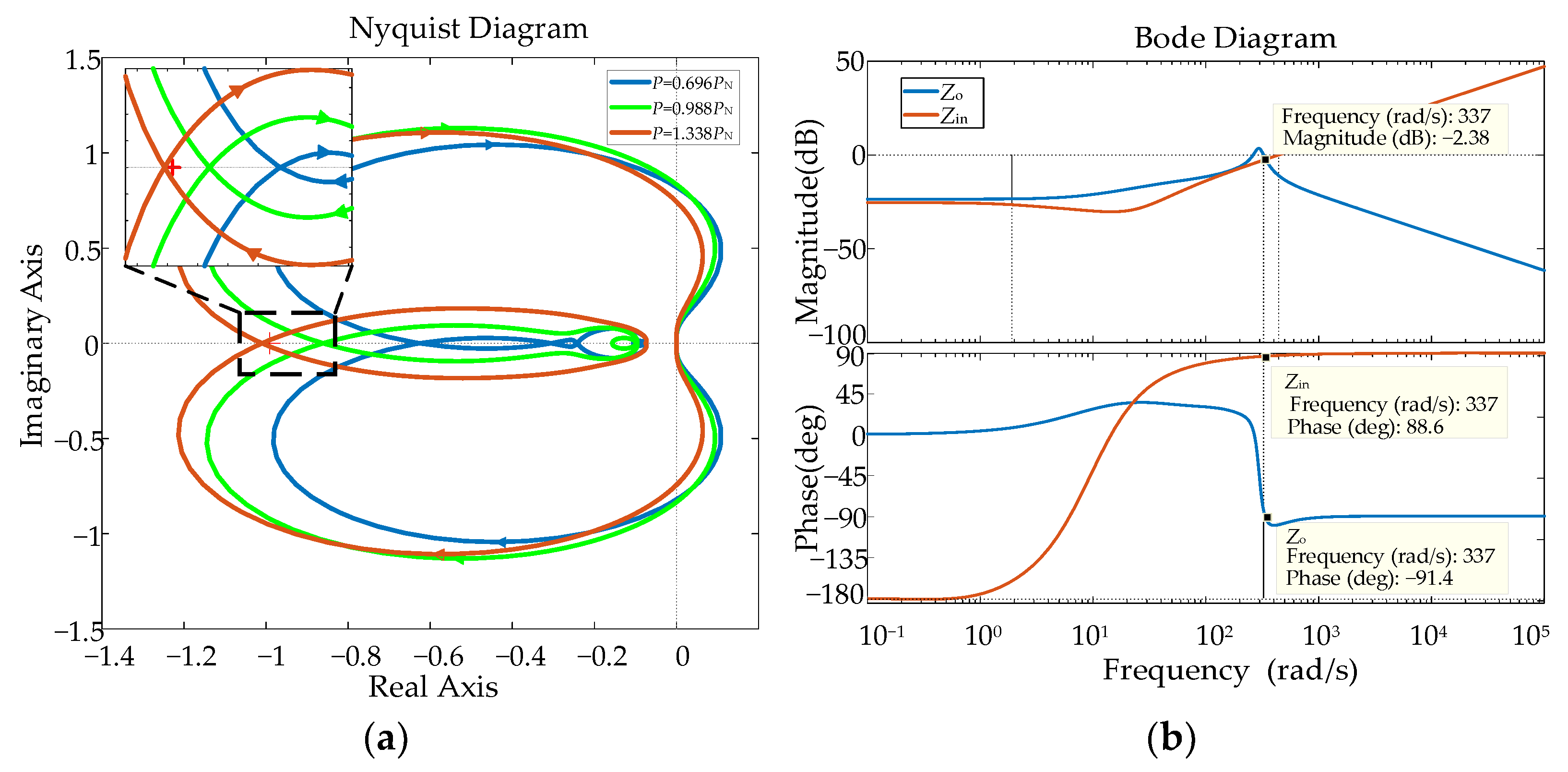
4.2. Analysis of Load Capacity

The cascade system composed of three rectifier modules connected in parallel and the EV charging load can be equivalent to the circuit in Figure 10.
The DC bus voltage can be expressed as:
V dc = Z in Z o + Z in G V gd = 1 T m + 1 G V gd
where
T m = Z o / Z in
According to (21) and (22), the DC bus voltage stability of the cascaded system depends on Tm, which can be determined by the ratio of the output impedance, Zo, of the source to the input impedance, Zin, of the load. The Nyquist curve of Tm and the frequency-domain response of input impedance, Zin, and output impedance, Zo, are shown in Figure 11.
From Figure 11a, when the load power P (the base value of load power PN = 180 kW) increases, the cascaded system could become unstable. According to the Nyquist stability criterion, when P = 1.338PN, the Nyquist curve surrounds the (−1, j0) point, indicating that the cascade system is unstable. Therefore, the maximum load capacity of the cascaded system is 240.8 kW. The frequency–domain response of input impedance, Zin, and output impedance, Zo, is shown in Figure 11b; when P = 1.338PN, the resonance frequency of system is 53.66 Hz.

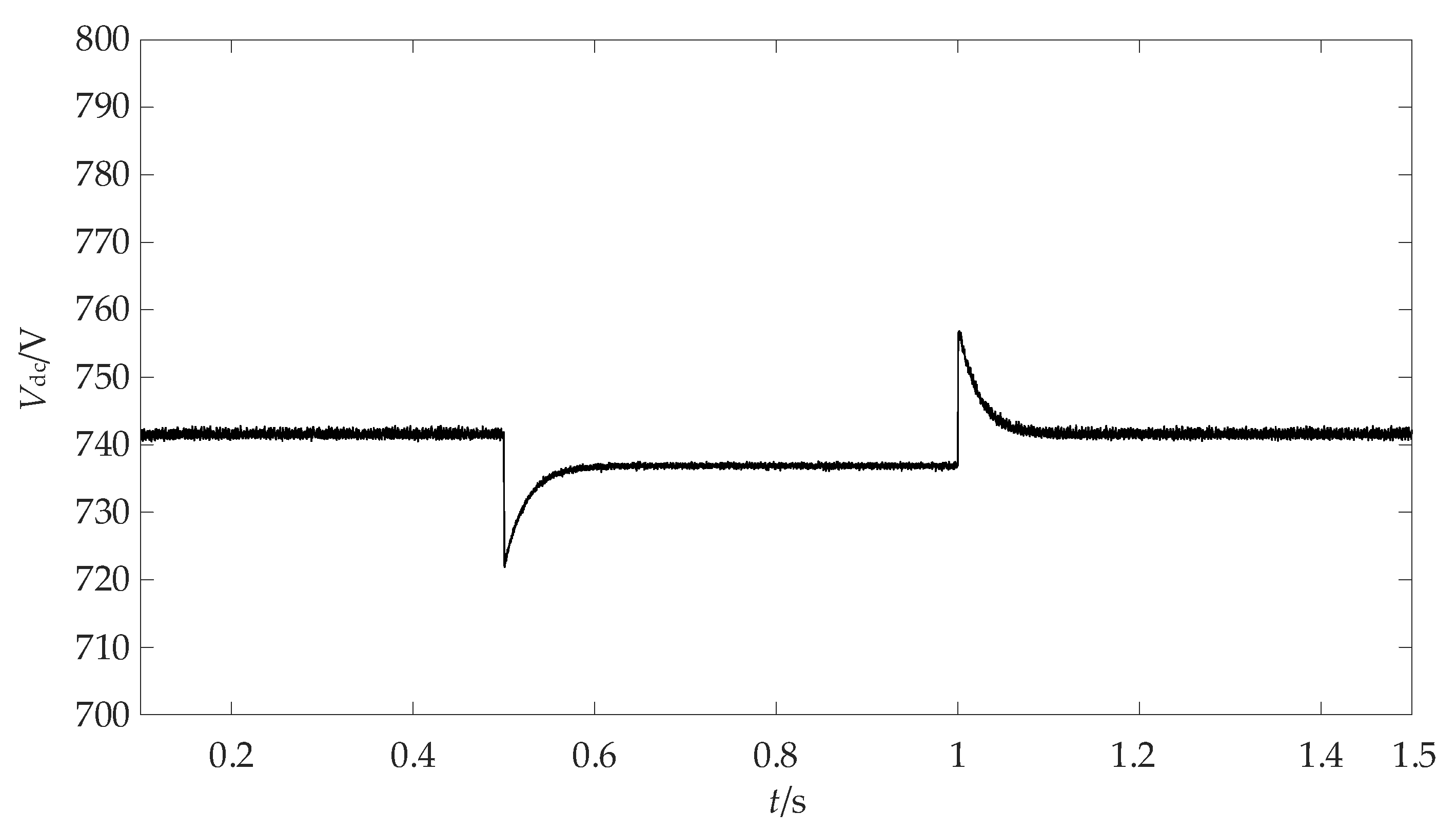
5. Simulation and Experimental Results

5.1. Simulation Results

In order to verify the correctness of the parameter design results of the power sharing controller and the theoretical analysis of the load capacity of the cascaded system, in the Matlab/simulink environment, a simulation model in which three controllable rectifier modules with a rated power of 60 kW are connected in parallel to perform charging for EV through a DC–DC converter, was generated. The simulation parameters of the main circuit and controllers are shown in Table 3.
The initial charging power of the EV is 90 kW, which increases to 180 kW in 0.5 s and decreases to 90 kW in 1 s. The waveforms of the output power, P1, P2, P3, and output current, idc1, idc2, idc3, of the three rectifier modules are shown in Figure 12. Because the virtual impedances of the three modules are the same, during the dynamic and steady-state process when the EV charging load increases from 90 kW to 180 kW, the three modules can achieve power sharing, and the output currents remain the same.
The waveform of the DC bus voltage is shown in Figure 13. Due to the effect of virtual impedance, the increase in the charging load will cause the DC bus voltage to drop, but it remains within the safe range of the design.
Figure 12 and Figure 13 illustrate that the three controllable rectifier modules achieve power sharing while maintaining the stability of the DC bus voltage, which proves the correctness of the current loop, voltage loop PI controller parameters, and virtual impedance design results.
The three parallel AC–DC controllable rectifiers all control the stability of the DC bus voltage. In order to verify the load capacity of the cascaded system composed of the DC–DC converter and the front three rectifiers, the change in the DC bus voltage is observed by gradually increasing the EV constant current charging load, as shown in Figure 14. When the EV constant current charging load increases from 0.5PN to 1.0PN and 1.3PN, the DC bus voltage can remain stable. When it increases to 1.4PN > 1.338PN, the DC bus voltage becomes unstable, which means that the cascaded system cannot bear such a large constant power load. This is consistent with the previous impedance analysis results.

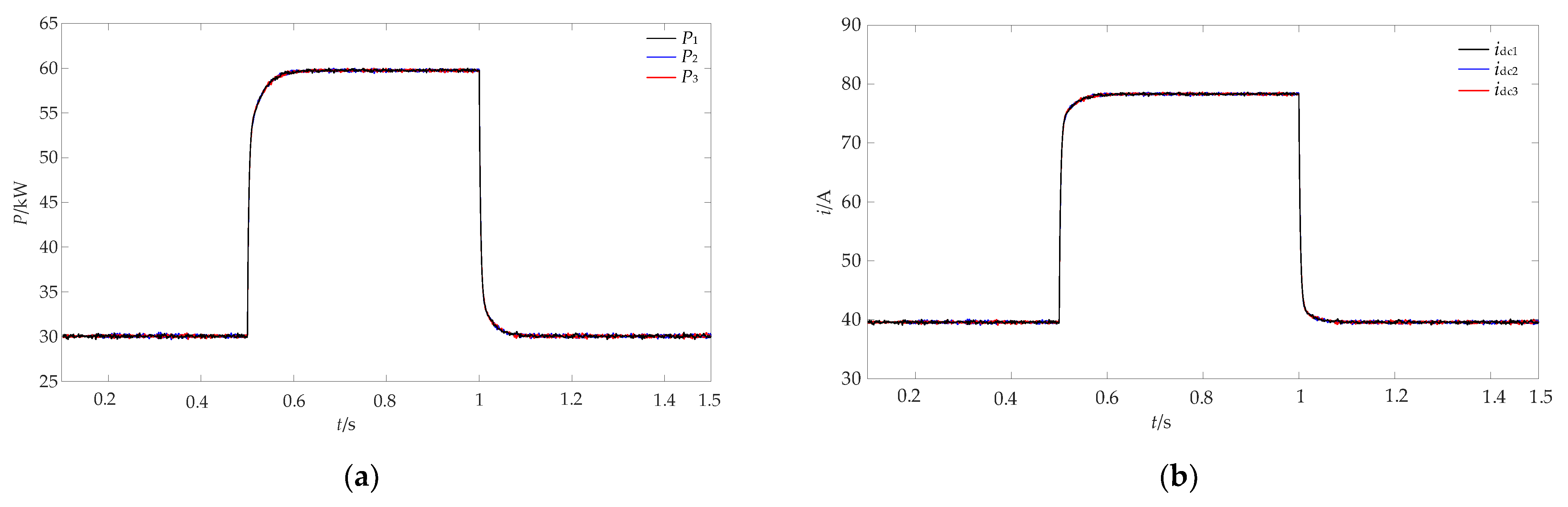
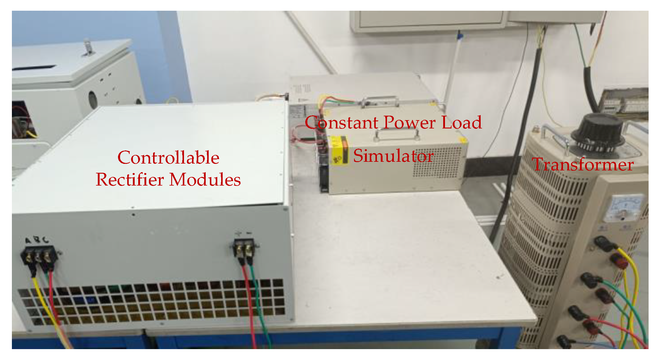
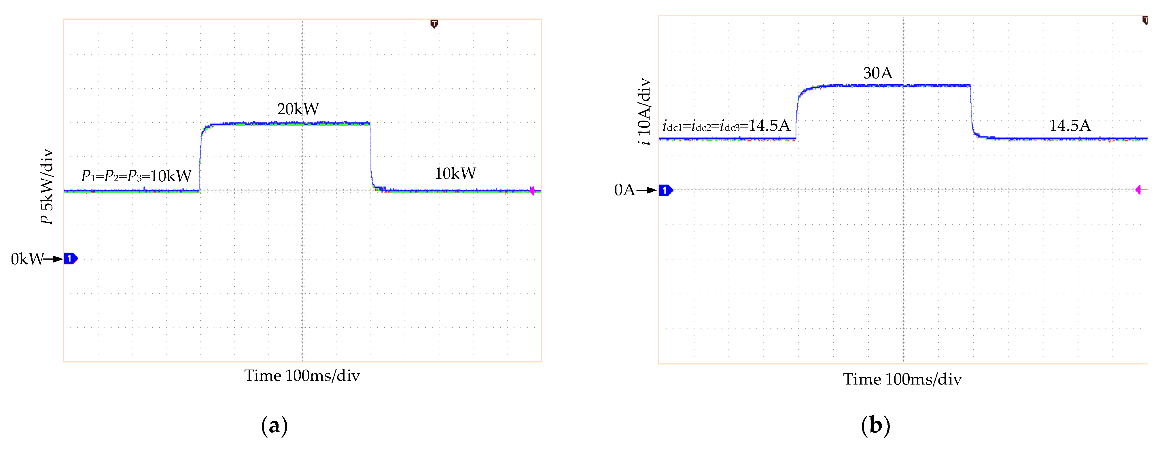
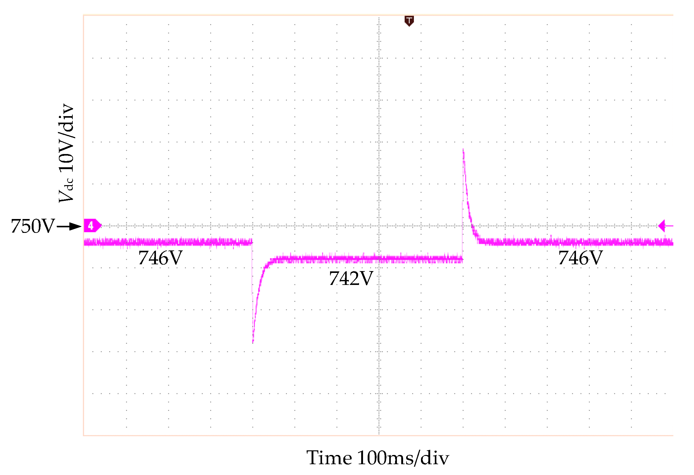
5.2. Experimental Results

To verify the simulation results, the experimental platform in Figure 15 is built, including the controllable rectifier modules, a constant power load simulator, and a transformer. Limited by the level of equipment in the lab, each module is rated at 20 kW and a constant power load simulator is used to simulate the EV charging load. The main circuit parameters and controller parameters of the experimental platform are shown in Table 4.
The initial total load is 30 kW, which then increases to 60 kW and decreases again to 30 kW. The waveforms of output power P1, P2 and P3 are shown in Figure 16a. The waveforms of output currents idc1, idc2 and idc3 are shown in Figure 16b. The three modules can achieve dynamic and steady-state power sharing, and the output currents can remain the same.
The waveform of the DC bus voltage is shown in Figure 17. When the load increases or decreases, the DC bus voltage can remain within a reasonable range. Figure 16 and Figure 17 illustrate that the experimental and simulation results are relatively consistent, which further verifies the effectiveness of the control strategy.

6. Conclusions

This paper studies the power sharing control method of a high-power DC fast charging station with three controllable rectifier modules connected in parallel. By designing the current loop and voltage loop PI controller parameters and virtual impedance, the dynamic and steady-state power sharing of different modules is realized. The proposed controller design method can be applied to the power distribution of n modules with the same or different rated capacities connected in parallel. In addition, the parallel AC–DC controllable rectifier modules, DC–DC converter, and EV charging loads constitute a cascade system. Considering that EVs can be equivalent to a constant power load when charging with a constant current, a constant voltage-controlled Buck converter with a resistive load is used to simulate the constant power load, and a mathematical model of its input impedance is established. The load carrying capacity of this cascaded system for EV charging with a constant current is studied by impedance analysis. The maximum bearable EV charging load of the cascade system is 1.35 times the rated capacity of the charging station. The experimental and simulation results prove the correctness of the controller design and stability analysis.

Author Contributions

Conceptualization, Z.-X.X.; methodology, J.-N.C.; software, J.-N.C. and H.-C.Z.; validation, P.L.; data curation, H.-F.X.; writing—original draft preparation, J.-N.C.; writing review and editing, Z.-X.X., G.-X.Z. and J.-W.J. All authors have read and agreed to the published version of the manuscript.

Funding

This research was funded by the National Natural Science Foundation of China (Grant No. 51977149) and Open Fund of Beijing Engineering Technology Research Center of Electric Vehicle Charging/Battery Swap (China Electric Power Research Institute) (No. YDB51202101508).

Data Availability Statement

The dataset used in this article can be obtained from the corresponding author under reasonable request.

Conflicts of Interest

The authors declare no conflict of interest.

Abbreviations

Abbreviations and Explanations:
EVElectric Vehicle
AC/DCAlternating Current/Direct Current
THDTotal Harmonic Distortion
PFCPower Factor Correction
DABDual Active Bridge
ZVSZero-Voltage Switching
IPQRImproved Proportional Quasi-Resonant
PIProportional Integral

References

  1. Tran, V.T.; Sutanto, D.; Muttaqi, K. The state of the art of battery charging infrastructure for electrical vehicles: Topologies, power controlstrategies, and future trend. In Proceedings of the Australasian Universities Power Engineering Conference, Melbourne, Australia, 19–22 November 2017. [Google Scholar]
  2. Erb, D.C.; Onar, O.C.; Khaligh, A. Bi-directional charging topologies for plug-in hybrid electric vehicles. In Proceedings of the IEEE Applied Power Electronics Conference & Exposition, Palm Springs, CA, USA, 21–25 February 2010. [Google Scholar]
  3. Du, S.; Lukic, S.; Jacobson, B.; Huang, A. Review of high power isolated bi-directional DC–DC converters for PHEV/EV DC charging infrastructure. In Proceedings of the IEEE Energy Conversion Congress and Exposition, Phoenix, AZ, USA, 10–14 October 2021. [Google Scholar]
  4. Vahedi, H.; Al-Haddad, K. A novel multilevel multioutput bidirectional active buck PFC rectifier. IEEE Trans. Ind. Electron. 2016, 63, 5442–5450. [Google Scholar] [CrossRef]
  5. Chen, Q.; Xu, J.; Wang, L.; Huang, R.; Ma, H. Analysis and improvement of the effect of distributed parasitic capacitance on high-frequency high-density three-phase buck rectifier. IEEE Trans. Power Electron. 2021, 36, 6415–6428. [Google Scholar] [CrossRef]
  6. Zhang, B.; Xie, S.; Li, Z. An optimized singlestage isolated Swiss-type AC/DC converter based on single full-bridge with midpoint-clamper. IEEE Trans. Power Electron. 2021, 36, 11288–11297. [Google Scholar] [CrossRef]
  7. Singh, A.K.; Jeyasankar, E.; Das, P. A matrix-based nonisolated three-phase AC–DC rectifier with large step-down voltage gain. IEEE Trans. Power Electron. 2017, 32, 4796–4811. [Google Scholar] [CrossRef]
  8. Ahmed, M.A.; Dasika, J.D. Interleaved Swiss rectiers for fast EV/PHEV battery chargers. In Proceedings of the IEEE Applied Power Electronics Conference & Exposition, Shanghai, China, 16–20 April 2014. [Google Scholar]
  9. Gowthamraj, R.; Aravind, C.V.; Prakash, O.K.S. Modeling of Vienna rectifier with PFC controller for electric vehicle charging stations. In Proceedings of the International Engineering Research Conference, Selangor Darul Ehsan, Malaysia, 3–4 July 2019. [Google Scholar]
  10. Zhang, L. A modified DPWM with neutral point voltage balance capability for three-phase Vienna rectifiers. IEEE Trans. Power Electron. 2021, 36, 263–273. [Google Scholar] [CrossRef]
  11. He, P.; Khaligh, A. Comprehensive analyses and comparison of 1 kW isolated DC–DC converters for bidirectional EV charging systems. IEEE Trans. Transp. Electrif. 2017, 3, 147–156. [Google Scholar] [CrossRef]
  12. Xuan, Y.; Yang, X.; Chen, W. A novel three-level CLLC resonant DC–DC converter for bidirectional EV charger in DC microgrids. IEEE Trans. Ind. Electron. 2021, 68, 2334–2344. [Google Scholar] [CrossRef]
  13. Yaqoob, M.; Loo, K.H.; Lai, Y.M. A four-degrees-of-freedom modulation strategy for dual-active-bridge series-resonant converter designed for total loss minimization. IEEE Trans. Power Electron. 2019, 34, 1065–1081. [Google Scholar] [CrossRef]
  14. Muthuraj, S.S.; Kanakesh, V.K.; Das, P. Triple phase shift control of an LLL tank based bidirectional dual active bridge converter. IEEE Trans. Power Electron. 2017, 32, 8035–8053. [Google Scholar] [CrossRef]
  15. Brand, M.J.; Hofmann, M.H.; Schuster, S.F. The influence of current ripples on the lifetime of lithium-ion batteries. IEEE Trans. Veh. Technol. 2018, 67, 10438–10445. [Google Scholar] [CrossRef]
  16. Zhang, M.; Yuan, Y.; Sun, X. Harmonic Resonance Suppression Strategy of the Front-End Vienna Rectifier in EV Charging Piles. IEEE Trans. Power Electron. 2022, 38, 1036–1053. [Google Scholar] [CrossRef]
  17. Wang, P.; Bi, Y.; Gao, F. An Improved Deadbeat Control Method for Single-Phase PWM Rectifiers in Charging System for EVs. IEEE Trans. Veh. Technol. 2019, 68, 9672–9681. [Google Scholar] [CrossRef]
  18. Song, T.; Wang, P.; Zhang, Y. Suppression Method of Current Harmonic for Three-Phase PWM Rectifier in EV Charging System. IEEE Trans. Veh. Technol. 2020, 69, 9634–9642. [Google Scholar] [CrossRef]
  19. Balasundar, C.; Sundarabalan, C.K.; Srinath, N.S. Interval Type2 Fuzzy Logic-Based Power Sharing Strategy for Hybrid Energy Storage System in Solar Powered Charging Station. IEEE Trans. Veh. Technol. 2021, 70, 12450–12461. [Google Scholar]
  20. Yan, D.; Chen, Y. A Distributed Online Algorithm for Promoting Energy Sharing between EV Charging Stations. IEEE Trans. Smart Grid 2023, 14, 1158–1172. [Google Scholar] [CrossRef]
  21. Zheng, Y.; Song, Y.; Hill, D.J. Online Distributed MPC-Based Optimal Scheduling for EV Charging Stations in Distribution Systems. IEEE Trans. Ind. Inform. 2019, 15, 638–649. [Google Scholar] [CrossRef]
  22. Yan, Q.; Zhang, B.; Kezunovic, M. Optimized Operational Cost Reduction for an EV Charging Station Integrated with Battery Energy Storage and PV Generation. IEEE Trans. Smart Grid 2019, 10, 2096–2106. [Google Scholar] [CrossRef]
  23. Sharma, J.S.; Guerrero, J.M. Effect of Fault Ride Through Capability on Electric Vehicle Charging Station Under Critical Voltage Conditions. IEEE Trans. Transp. Electrif. 2022, 8, 2469–2478. [Google Scholar]
  24. Lenka, R.K.; Panda, A.K.; Patel, R. PV Integrated Multifunctional Off-Board EV Charger with Improved Grid Power Quality. IEEE Trans. Ind. Appl. 2022, 58, 5520–5532. [Google Scholar] [CrossRef]
  25. Engel, J.; Schmitt, T.; Rodemann, T. Hierarchical Economic Model Predictive Control Approach for a Building Energy Management System with Scenario-Driven EV Charging. IEEE Trans. Smart Grid 2022, 13, 3082–3093. [Google Scholar] [CrossRef]
  26. Kriukov, A.; Gavrilas, M.; Ivanov, O. Novel Decentralized Voltage-Centered EV Charging Control Algorithm Using DSRC System in Low Voltage Distribution Networks. IEEE Access 2021, 9, 164779–164800. [Google Scholar] [CrossRef]
  27. Cittanti, D.; Gregorio, M.; Vico, E. High-Performance Digital Multiloop Control of LLC Resonant Converters for EV Fast Charging with LUT-Based Feedforward and Adaptive Gain. IEEE Trans. Ind. Appl. 2022, 58, 6266–6285. [Google Scholar] [CrossRef]
Figure 1. Typical DC fast charging station topology.
Wevj 14 00193 g001
Figure 2. High-power DC fast charging station topology and controller structure.
Wevj 14 00193 g002
Figure 3. Transfer function model of each rectifier module.
Wevj 14 00193 g003
Figure 4. Bode diagram and step response of current loop changing with kpi and kii. (a) Bode diagram of Gio changing with kpi. (b) Step response of Gic changing with kpi. (c) Bode diagram of Gio changing with kii. (d) Step response of Gic changing with kii.
Wevj 14 00193 g004
Figure 5. Bode diagram and step response in voltage loop changing with kpu and kiu. (a) Bode diagram of Guo changing with kpu. (b) Step response of Guc changing with kpu. (c) Bode diagram of Guo changing with kiu. (d) Step response of Guc changing with kiu.
Wevj 14 00193 g005
Figure 6. Frequency–domain response of output impedance, Zno. (a) Frequency–domain response of Zno when kpu changes. (b) Frequency–domain response of Zno when kiu changes.
Wevj 14 00193 g006
Figure 7. Virtual impedance design. (a) Virtual impedance design principle. (b) Output impedance after adding virtual impedance.
Wevj 14 00193 g007
Figure 8. Equivalent circuit of a constant power load.
Wevj 14 00193 g008
Figure 9. Buck converter transfer function model.
Wevj 14 00193 g009
Figure 10. Equivalent circuit of the cascaded system.
Wevj 14 00193 g010
Figure 11. Nyquist curve and frequency–domain response of the cascaded system. (a) Nyquist curve of Tm when the load P changes. (b) Input impedance Zin and output impedance Zo when P = 1.338PN.
Wevj 14 00193 g011
Figure 12. Output power and currents of the rectifier modules. (a) Output power. (b) Output current.
Wevj 14 00193 g012
Figure 13. The DC bus voltage waveform during power sharing.
Wevj 14 00193 g013
Figure 14. The DC bus voltage waveform when adding a constant power load.
Wevj 14 00193 g014
Figure 15. Experimental platform.
Wevj 14 00193 g015
Figure 16. Output power and currents of the rectifier modules. (a) Output power. (b) Output current.
Wevj 14 00193 g016
Figure 17. The DC bus voltage waveform during power sharing.
Wevj 14 00193 g017
Table 1. Dynamic and steady-state performance indicators of the current loop when kpi and kii change.
kii = 100
kpiGain Margin (dB)Phase Margin (deg)Bandwidth(kHz)Overshoot (%)Response TimeSteady-State Error
0.01−9.85−9.930.14unstableunstableunstable
0.1Inf26.10.1550.067.8 × 10−4
1Inf83.50.660.220.051.8 × 10−3
3.5Inf88.52.2806 × 10−41.5 × 10⁻³
7Inf89.34.5503 × 10−46.4 × 10⁻³
kpi = 3.5
kiiGain margin (dB)Phase margin (deg)Bandwidth(kHz)Overshoot (%)Response timeSteady-state error
1Inf88.72.2806 × 10−45.5 × 10⁻³
10Inf88.62.2806 × 10−45.7 × 10⁻³
100Inf88.52.2816 × 10−41.5 × 10⁻³
300Inf88.22.281.54 × 10−33.9 × 10⁻²
1000Inf872.283.20.0126 × 10−4
Table 2. Dynamic and steady-state performance indicators of the voltage loop when kpu and kiu change.
kiu = 150
kpuGain Margin (dB)Phase Margin (deg)Bandwidth (Hz)Overshoot (%)Response Time (s)Steady-State Error
0.118.175.214.500.075.2 × 10−3
117.496.417.800.095.2 × 10−4
1.713.711242.700.144 × 10−4
39.2371.686.100.161 × 10−3
72.2112.9152.746.50.355 × 10−4
10−0.816−4.54192.7unstableunstableunstable
kpu = 1.7
kiuGain margin (dB)Phase margin (deg)Bandwidth (Hz)Overshoot (%)Response time (s)Steady-state error
1014.713727.702.51.15 × 10−3
10014.112037.400.253.5 × 10−4
15013.711242.700.144 × 10−4
30012.489.451.600.062.1 × 10−3
10004.2420.977.554.30.11.3 × 10−3
Table 3. Simulation parameters of the main circuit and controllers.
Each Rectifier Module ParametersValue
RMS value of grid line voltage Vg/V380
Filter inductor Ls/mH0.3
DC side capacitance C/mF1
Inductors connected in parallel L/mH1
The internal resistance of the inductance connected in parallel R0.001
Current loop PI controller parameters/kpi, kii3.5, 100
Voltage loop PI controller parameters/kpu, kiu1.7, 150
Rated power PN/kW60
Virtual impedance Zv0.2
Reference value of DC bus voltage Vdc*/V750
Buck converter parametersValue
Filter inductor LL/mH3.33
Filter inductor internal resistance rL0.001
Load side capacitance CL/mF0.2
Reference value of load voltage UL*/V500
Voltage loop PI controller parameters/kpuL, kiuL0.0005, 0.4
Table 4. Experimental parameters of the main circuit and controllers.
Each Rectifier Module ParameterValue
RMS value of grid line voltage Vg/V380
Filter inductor Ls/mH0.5
DC side capacitance C/mF2
Inductors connected in parallel L/mH0.5
The internal resistance of the inductance connected in parallel R0.02
Current loop PI controller parameters/kpi, kii3, 200
Voltage loop PI controller parameters/kpu, kiu1, 100
Rated power PN/kW20
Virtual impedance Zv0.1
Reference value of DC bus voltage Vdc*/V750
Disclaimer/Publisher’s Note: The statements, opinions and data contained in all publications are solely those of the individual author(s) and contributor(s) and not of MDPI and/or the editor(s). MDPI and/or the editor(s) disclaim responsibility for any injury to people or property resulting from any ideas, methods, instructions or products referred to in the content.

