1. Introduction
When oxidized, copper can form three types of oxides, namely: cuprous oxide (Cu
2O, cuprite), cupric oxide (CuO, tenorite) and Cu
4O
3 (paramelaconite) [
1]. All three forms of copper oxides are semiconductors, and Cu
2O, in particular, is one of the first semiconductors studied for device applications. In the early 20th century, Cu
2O Schottky junctions were intensively investigated for use as rectifiers in radio receivers [
2]. A review of the research conducted during this period, including the difficulty of n-type doping, was written by Brattain in 1950 [
3]. After the invention of the point contact transistor in 1947 and the metal oxide semiconductor field-effect transistor in 1960, interest in Cu
2O declined because of the availability of single crystal silicon and germanium, which can be doped n- and p-type [
2]. During the 1970s, there was a resurgence of interest in Cu
2O as a semiconductor for photovoltaics (PV) because of the need to develop terrestrial PV devices for solar energy conversion in response to the first oil crisis of 1973. The Cu
2O solar cells investigated during this period were Schottky junction PV devices [
4,
5,
6]. Two research projects on these devices supported by the U.S. National Science Foundation were carried out at the Joint Center for Graduate Study [
5,
6]. This focus on the Schottky junction structure was due to the difficulty of forming p-n homojunctions in Cu
2O. Owing to chemical reduction of the Cu
2O surface to Cu during sputter deposition, the best η obtained was only of the order of 1% regardless of the metal deposited [
6]. Nevertheless, it was recognized that a heterojunction or metal-inuslator-semiconductor structure should improve the performance of Cu
2O PV devices. The low η that could be achieved in these Cu
2O PV devices eventually led to another waning of interest by the 1980s. A review of the literature on Cu
2O Schottky junction devices during this period can be found in [
7]. Despite this, research on Cu
2O PV devices continued in Japan, Italy and elsewhere after the 1990s. The Cu
2O PV research in this recent period is concerned with a search for newer dopants for Cu
2O, suitable transparent n-type semiconductors for heterojunction formation and low damage junction formation techniques. As a result, there has been significant improvements in the reported η of Cu
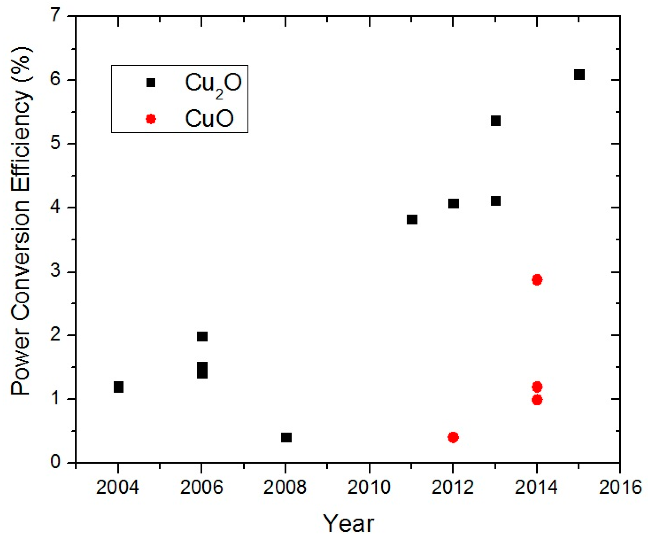
2O PV devices. This can be seen from
Figure 1, which is based on a compilation of published η values in the PV literature [
8]. In 2015, an η value of 6% was reported for a heterojunction PV device based on Cu
2O and another n-type semiconductor. This value is exactly triple that of the best η value reported in 2006 for a Cu
2O heterojunction PV device (see
Section 3).
Figure 1 shows that, in addition to Cu
2O, there has been growing research interest in CuO PV devices in recent years. The highest reported η as of 2015 for a CuO based PV device is 1.2%.
It is useful to first consider why an old semiconductor such as copper oxide still attracts such a niche interest at a time when many new semiconductors such as the perovskite and organic semiconductors are being studied for PV applications. In the latest solar cell efficiency tables (version 47) [
9], there is no listing for copper oxide devices. Textbooks on PV devices usually have no coverage of copper oxide PV devices [
10,
11]. The main exception is the reference by Fonash, which has brief mention of Cu
2O [
12]. Sustainability is the main reason for the sustained interest in the copper oxides for PV. Both copper and oxygen are abundant elements like silicon and thus there can be no supply concern in the long run [
13]. This is one of the four requirements for a semiconductor to be usable for large scale PV power generation [
14]. As discussed extensively in [
15,
16], a careful sustainability analysis of a large number of semiconductor materials showed that Cu
2O and CuO are sustainable PV materials. In addition, all three oxides of copper are non-toxic and can be deposited as thin films relatively simply at low cost. The copper oxides are p-type oxide semiconductors uniquely suitable for PV applications. Although there are a few alternative p-type binary oxides such as tin monoxide (SnO) and nickel oxide (NiO), their energy band gaps of 2.5 eV and 3.6–4.0 eV, respectively, are too wide for PV applications [
17]. Hence, at present, these transition metal oxides are mainly used for transparent semiconductors.
This review will focus on recent developments in copper oxide heterojunction solar cells and complements the earlier review by Rakhshani [
7]. It is organized into seven sections. In
Section 2, we first outline the theory of heterojunction solar cells with emphasis on the copper oxide heterojunction and band diagram.
Section 3 and
Section 4 review the Cu
2O and CuO heterojunction solar cells, respectively.
Section 5 describes the electrodeposited Cu
2O/CuO heterojunction and its PV properties.
Section 6 will briefly discuss preliminary studies on solar cells based on Cu
4O
3. This is followed by a conclusion and outlook on the remaining challenges in the field of copper oxide solar cells.
2. Heterojunction Solar Cell Device Physics
Before reviewing the copper oxide heterojunction solar cells, it is useful to consider the energy band diagram and the theory of heterojunction solar cells. Cu
2O and CuO form type II heterojunctions with another semiconductor such as ZnO or Si in these solar cells. In a type II (or staggered) heterojunction, only one of the band edges (either
Ec or
Ev) of one semiconductor is situated within the band gap of the other semiconductor forming the heterojunction [
12].
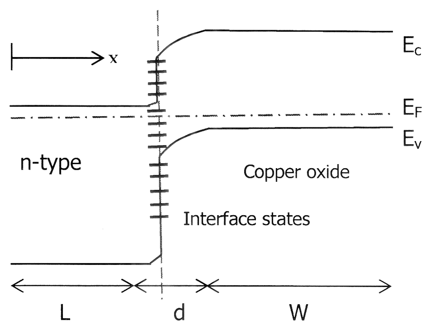
Figure 2 illustrates the schematic energy band diagram of a copper oxide n-type semiconductor heterojunction with interface defects to be discussed in the next section. The n-type layer has the wider energy gap in this heterojunction and therefore sun light is incident through this window layer to reach the Cu
2O substrate. There is band bending on both sides of this junction and the built-in electric field separates the photo-generated electrons and holes as in a homojunction solar cell. By applying the one-dimensional theory of the semiconductor-semiconductor heterojunction cell in [
12], the current density
J from the device under illumination can be written as:
Here,
q is the electronic charge;
d is the thickness of the neutral p-type layer;
W is the depletion layer width and
L is the thickness of the neutral n-type layer. The free carrier photogeneration function,
Gph is integrated with respect to wavelength over the full spectrum of incident sunlight and over the thickness of the solar cell.
R represents the rate of recombination in the neutral bulk regions of the p- and n-type regions of the heterojunction.
JST and
JSB are the reductions in current density due to recombination in the top and bottom contacts, respectively. The last term
JIR on the right hand side of Equation (1) is unique to heterojunction solar cells and accounts for recombination at the heterojunction interface. Although another closed form analytical expression for the current density of the heterojunction solar cell exists [
18], the equation given above especially shows clearly the effects of recombination on the current density obtainable from the heterojunction solar cell.
The rate of recombination is characterized by the minority carrier lifetime
τn. For a p-type semiconductor with dopant density
NA,
τn is given by:
Here,
B is the radiative recombination coefficient [
19]:
where
h is the Planck constant;
k is the Boltzmann constant;
T is the absolute temperature and
c is the speed of light.
m is the free electron mass and
me and
mh are the electron and hole effective mass, respectively.
n is the refractive index and
Eg is the energy band gap of the semiconductor. The quadratic dependence of
B on
Eg shows that a semiconductor with a narrower band gap will have a longer minority carrier lifetime. On the other hand, a lower dopant density can also increase
τn.
In addition to the reduction in current density, the main effect of carrier recombination within a heterojunction solar cell is a decrease in the open circuit voltage,
Voc. For a p-type layer thickness of
w and low level excitation conditions,
Voc is given by [
20]:
where
Nc and
Nv are the effective density of states for the conduction band and valence band, respectively, and
Jph is the photocurrent density. The second term of this equation shows that for both increased
B and reduced
Jph, the magnitude of
Voc is reduced. This shows the crucial impact of recombination on the photovoltaic performance of heterojunction solar cells.
3. Cu2O Thin Film Heterojunction Solar Cells
Cu
2O can be formed by thermal oxidation of high purity Cu foils in a furnace [
21]. The material properties of Cu
2O have been studied in detail and can be found in other reviews [
1]. Here, for the sake of completeness, only a summary of those properties of Cu
2O relevant to solar cells will be described. Cu
2O has a cubic unit cell structure and an energy band gap of 1.7–2 eV depending on the deposition conditions [
1]. Since the band gap of Cu
2O is direct, the absorption coefficient of Cu
2O is relatively high (~10
5 cm
−1) and is comparable to some organic semiconductors. As-deposited undoped Cu
2O is a p-type semiconductor with a majority carrier mobility of ~100 cm
2/V∙s. The p-type conductivity is due to Cu vacancies in the Cu
2O [
1]. For extrinsic doping, N and Cl are known to be p-type dopants for Cu
2O [
22]. The search for n-type dopants for Cu
2O has until recently been elusive [
3]. However, as will be discussed in
Section 4 and
Section 5, respectively, methods for preparing n-type CuO
x and Cu
2O are now available.
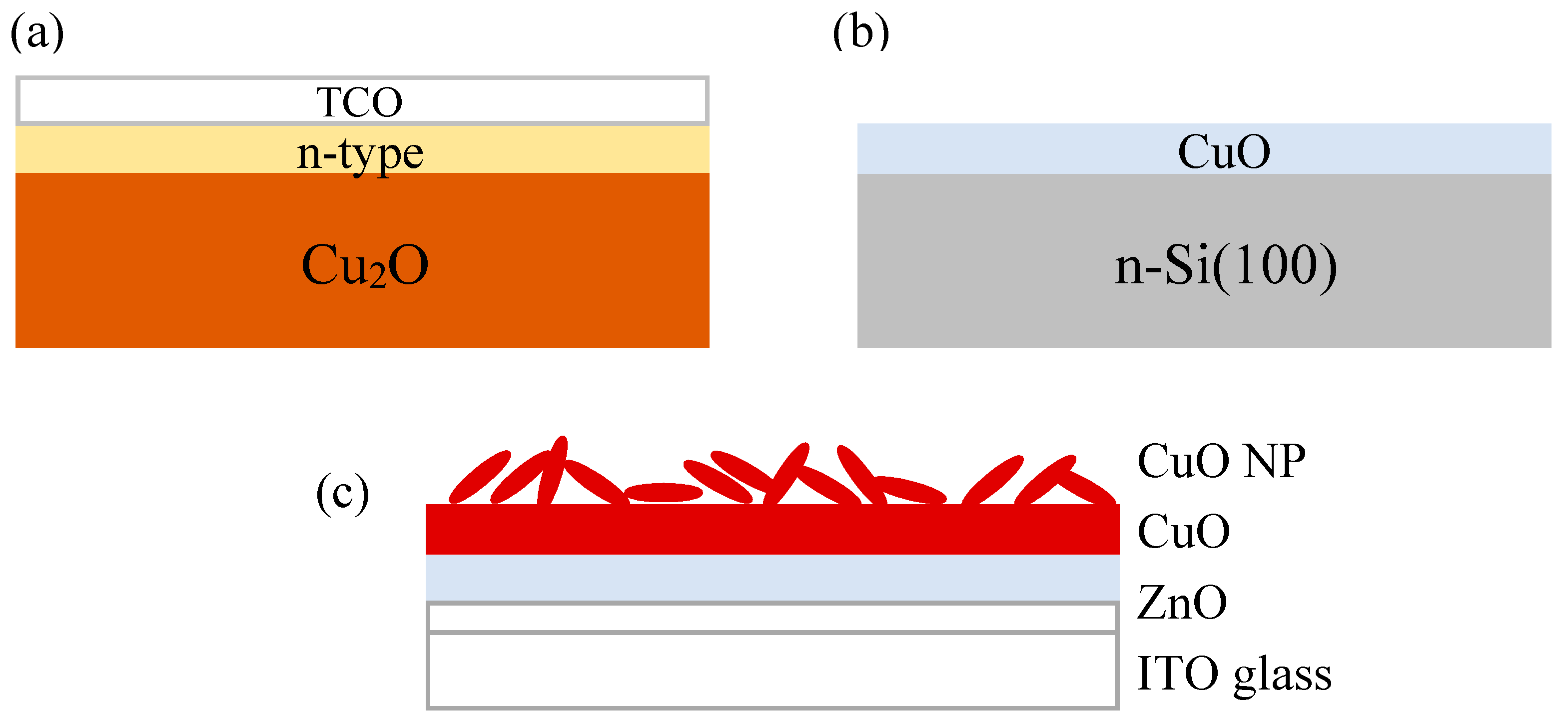
Cu
2O heterojunction solar cells have a device structure similar to other thin film solar cells (
Figure 3a). The Cu
2O is both the absorber and a substrate upon which is deposited a thin layer of n-type wide band gap semiconductor. This layer may have a third transparent conducting oxide (TCO) layer deposited on top of it. Ohmic contacts are formed to both the top and bottom of the device. The first published report of Cu
2O heterojunction solar cells with this structure was that by Herion
et al. in 1980 [
23]. These investigators used the sputtering technique to deposit ZnO onto Cu
2O sheets. The PV characteristics of this device is tabulated in
Table 1 (see Section 5) together with other key devices discussed in this review. Although an η of 0.14% was measured for the ZnO-Cu
2O device, the photovoltaic effect was not due to a ZnO-Cu
2O heterojunction. Rather, it was due to the Schottky barrier between a thin Cu film formed by reduction of the Cu
2O surface during the ZnO sputter deposition. This paper highlights the susceptibility of the Cu
2O surface to solid state reaction and hence the need to choose a low energy, low damage deposition method to form a true semiconductor heterojunction with Cu
2O.
A more recent example of a thin film p-Cu
2O/n-ZnO heterojunction solar cell fabricated on glass substrates by sputtering is the work of Akimoto
et al. [
24]. In this study, the Cu
2O layer was deposited by reactive radio frequency (rf) magnetron sputtering using a Cu target while the ZnO layer was deposited by magnetron sputtering. The sequence of deposition was found to have a major influence on the photovoltaic properties of the heterojunction fabrication. For the glass/Au/p-Cu
2O/i-ZnO/n-ZnO (Cu
2O first) structure, the reverse leakage current was relatively high and a photovoltaic effect was almost unobservable [
24]. On the other hand, the glass/n-ZnO/i-ZnO/p-Cu
2O (ZnO first) structure showed much better rectification and an η of 0.4% was obtained [
24]. The difference between the two device structures was attributed to the similar atomic arrangements in the crystal structures of ZnO and the Cu
2O for the ZnO first structure, which results in fewer interface defects. However, both
Voc and short circuit current density
Jsc are low because of these defects.
In order to achieve η above 1%, it is necessary to identify suitable n-type semiconductors that can be deposited onto Cu
2O [
25]. This is because solar cells fabricated from Cu
2O substrates tend to have higher efficiency than cells made from Cu
2O thin films [
7]. In one such study [
26], Tanaka
et al. deposited several transparent conducting oxides (TCO) thin films, namely In
2O
3, In
2O
3:Sn (ITO), ZnO, ZnO:Al (AZO) and ZnO-In
2O
3 by PLD onto Cu
2O sheets. Both In
2O
3 and ITO gave poorly rectifying heterojunctions and poor PV performance. ZnO-Cu
2O formed rectifying junctions and the current voltage characteristics both in the dark and under illumination were found to be affected by the O
2 pressure during deposition [
26]. The highest η obtained for ZnO-Cu
2O was 0.9% under illumination by air mass AM 2 solar spectrum. On the other hand, an η of over 1% can be achieved by using the AZO-Cu
2O heterojunction. This is because AZO has a smaller work function than ZnO [
26]. For AZO, the critical parameter is the deposition temperature during PLD. By controlling this temperature to the range of 150 °C–200 °C, a rectifying junction and an η of 1.2% under AM2 illumination was obtained. The improvement in η of the AZO-Cu
2O junction is attributed to a broader spectral response that results in higher
Jsc [
26]. The results of refs [
25] and [
26] show that ZnO and AZO are suitable n-type semiconductors for forming heterojunctions with Cu
2O.
Until 2006, the η of Cu
2O heterojunction solar cells reported in the literature remained under 2%. Since this is obviously inferior to competing second generation semiconductor solar technologies and much lower than the theoretical limit of Cu
2O devices of 20% for the AM1 spectrum [
5], systematic studies were carried out to improve the fabrication technique of the Cu
2O cells. In one such study, Minami
et al. investigated four techniques for depositing the n-type thin film semiconductor on a Cu
2O absorber substrate [
27]. These include: (i) DC magnetron sputtering; (ii) rf magnetron sputtering; (iii) PLD and (iv) vacuum arc plasma evaporation (VAPE). The VAPE technique involves the use of a low voltage discharge to generate an arc plasma to evaporate the source material [
28]. AZO was deposited by DC and RF magnetron sputtering at different substrate temperatures and for different sample orientation and positions in the sputtering system. The film properties of the AZO such as crystallinity, carrier concentration, Hall mobility and resistivity were all strongly dependent on the substrate temperature and sample orientation. Since the properties of the AZO film affect the properties of the AZO/Cu
2O junction, the photovoltaic parameters show a similar dependence on deposition conditions. It was concluded that at the optimum substrate temperature and for a sample normal to the target, the improved PV performance was a result of fewer defects at the heterojunction and an improved crystallinity of the AZO [
27]. This in turn suggests that magnetron sputtering, DC or RF, may not be the best deposition technique for forming the AZO/Cu
2O heterojunction. PLD and VAPE were therefore used to deposit ZnO on Cu
2O in addition to DC and RF magnetron sputtering. Both PLD and VAPE do not involve ion bombardment of the Cu
2O surface which can generate electronic defects. Furthermore, the absence of reactive oxygen species preclude the oxidation of the Cu
2O surface [
27]. As a result, the η of ZnO/Cu
2O devices fabricated by PLD (1.42%) and by VAPE (1.52%) were both higher than devices fabricated by magnetron sputtering [
27]. This is the reason why the highest performance Cu
2O heterojunction devices are usually fabricated by PLD nowadays.
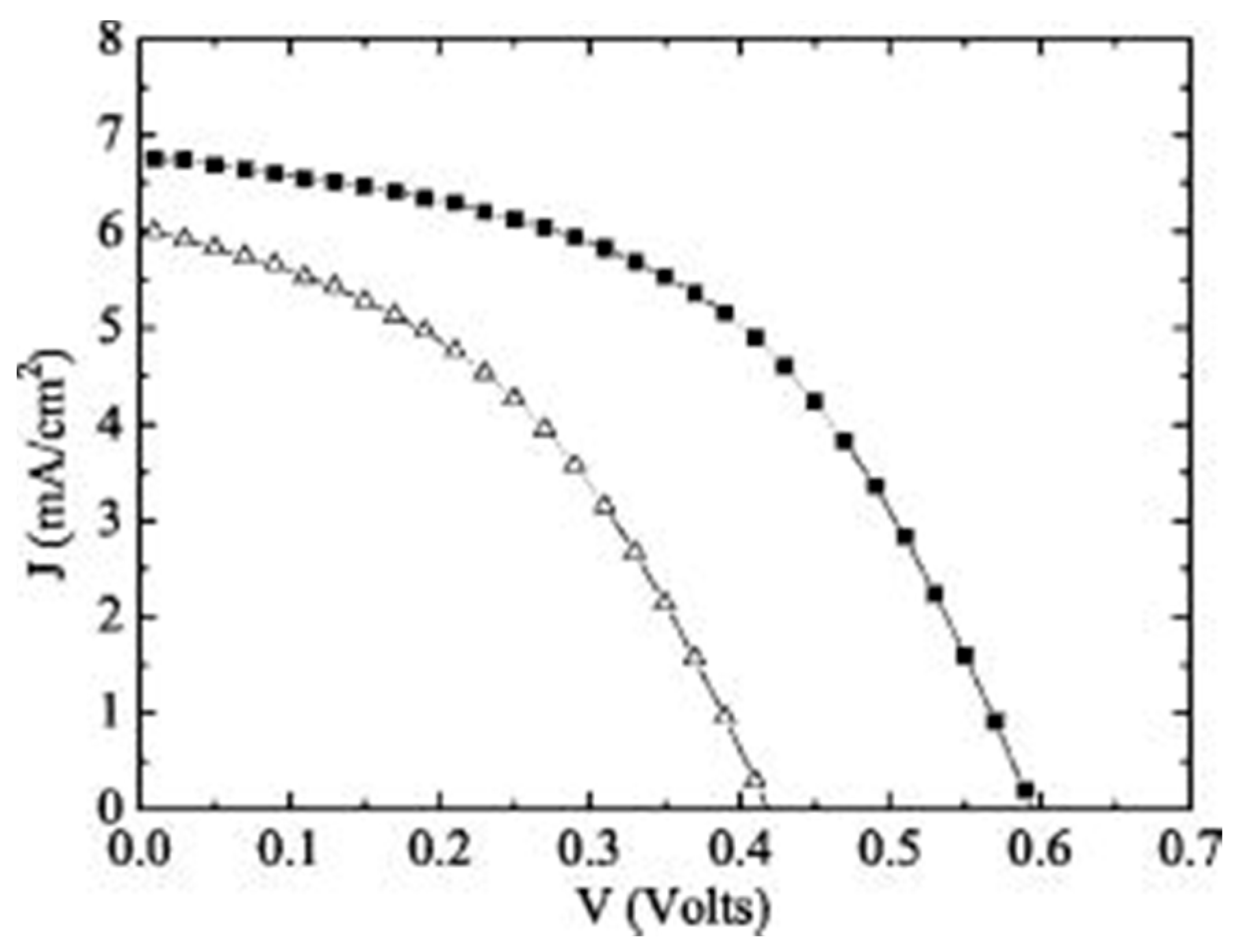
A Cu
2O heterojunction solar cell with an η above 2% was reported by Mittiga
et al. in 2006 [
29]. This device has a four layer structure and consists of a thermally oxidized Cu
2O substrate, a ZnO n-type layer, an indium doped tin oxide (ITO) window layer and an antireflection MgF
2 layer. The oxidation conditions used for the Cu
2O layer resulted in a polycrystalline structure with large grain size and high hole mobility. A low resistivity (~1 kΩm) was realized by quenching the Cu
2O sheets after cooling to 450 °C in a furnace [
29]. The ZnO layer was deposited onto the Cu
2O substrate by ion beam sputtering (IBS) followed by a thicker layer of ITO deposited by the same technique. Under AM 1.5G (global) illumination, the Au/Cu
2O/ZnO/ITO/MgF
2 device has a measured η of 2.01% [
29]. This was higher than the reference Au/Cu
2O/ITO/MgF
2 device as shown by the
J-V characteristics in
Figure 4. The
Voc values for both devices were considered to be influenced by defects at the heterointerface. These cause reduction in the shunt resistance and increased the reverse saturation current. As a result, improvement of interface defects should increase the
Voc and η.
The first report of a Cu
2O heterojunction solar cell with an η above 3% was reported by the Kanazawa Institute of Technology in 2011. In the first of a series of papers [
30,
31,
32,
33], Minami and co-workers demonstrated an improved device architecture for Cu
2O devices. In this structure, a polycrystalline Cu
2O substrate and absorber was first formed from Cu by using a three step oxidation process [
30]. Subsequently, an n-type layer of undoped ZnO and a transparent conductor layer of AZO were deposited sequentially by PLD. The ZnO forms a heterojunction with Cu
2O and the AZO acts as a window layer. The back contact consists of an ohmic contact formed from either Au or Cu
2S. The photovoltaic parameters
Voc,
Jsc, fill factor
FF and η were studied as a function of the ZnO layer thickness. For a ZnO thickness in the range of 30–50 nm, the η reached a maximum of 3.83% [
30]. This was mainly due to improvement in ZnO film properties such as fewer interface defects and reduced resistivity. For a ZnO layer thicker than 50 nm, both
Voc and FF decreased because of a short minority carrier lifetime [
30]. By comparison, the η of an AZO/Cu
2O reference device of ~1.6% was lower than the optimized AZO/ZnO/Cu
2O device. This shows that the ZnO buffer layer forms a better quality junction with Cu
2O in comparison with AZO. However, both the deposition condition and thickness of the ZnO layer must be carefully controlled to obtain high efficiency.
A more in-depth study of the n
+AZO/ZnO/Cu
2O device structure was carried out by Nishi
et al. [
31]. The device fabrication process was similar to that in [
30]. The thickness of the ZnO buffer layer was varied between 0 nm and 150 nm where a zero ZnO thickness corresponded to an n
+AZO/Cu
2O Schottky barrier junction. At the optimum ZnO thickness of 50 nm, an η of 4.08% was measured. Dark current voltage measurements showed that the inserted ZnO buffer layer forms a heterojunction with the Cu
2O with a built in potential (or barrier height) that is greater than that of the Schottky junction. The increased barrier height could be related to the higher quality interface obtained when ZnO is deposited at room temperature conditions [
31]. In addition, the lower carrier concentration of the undoped ZnO layer results in a finite depletion width in the ZnO that increases the total active layer thickness. This is shown by photovoltage spectral response measurement. When compared with the n
+AZO/Cu
2O device, the n
+AZO/ZnO/Cu
2O device has a broader photovoltage spectrum below 460 nm because of the heterojunction formation [
31].
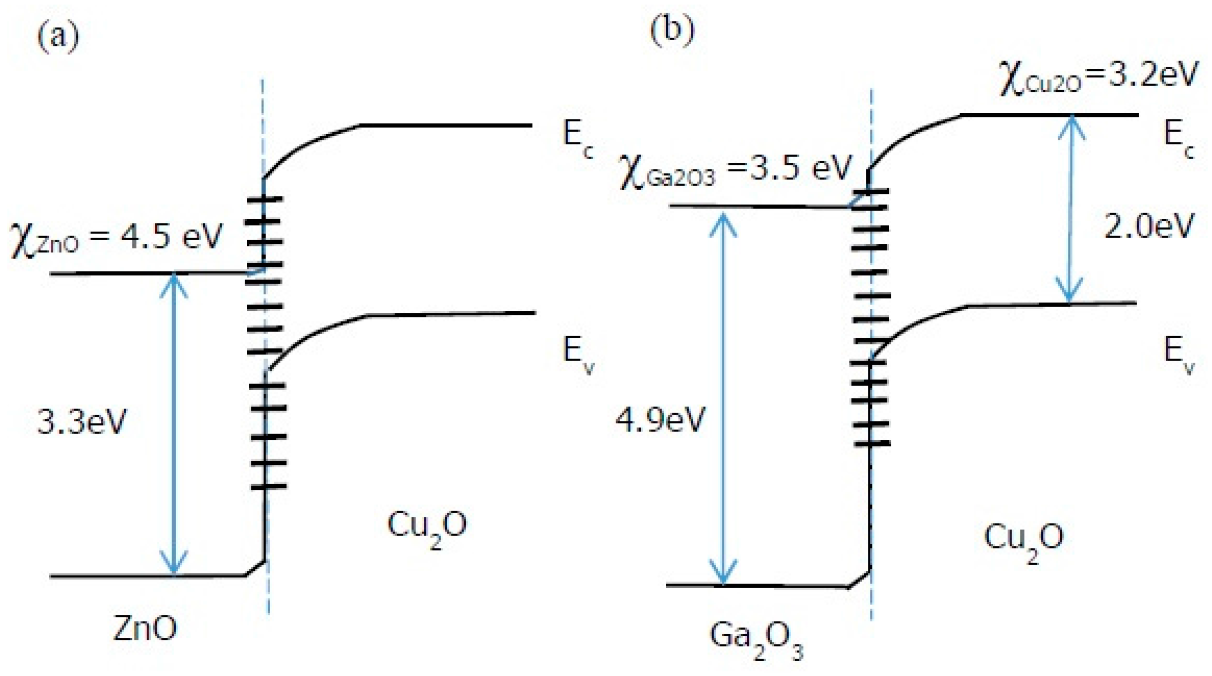
A still higher η was obtained by Minami
et al. when the undoped ZnO layer was substituted by undoped n-type Ga
2O
3 in an AZO/Ga
2O
3/Cu
2O/Au device structure [
32]. The choice of Ga
2O
3 was motivated by the fact that the photovoltaic properties of a Cu
2O heterojunction cell are determined by the energetics of the heterointerface. For the Ga
2O
3/Cu
2O heterojunction, the conduction band offset (Δ
Ec) is smaller because the electron affinity
χ of Ga
2O
3 is in between that of Cu
2O and ZnO (
Figure 5) [
32,
33]. This smaller Δ
Ec should lead to a higher device efficiency. The Ga
2O
3 layer in this device was also deposited by PLD using Ga
2O
3 pellets in the presence of oxygen. The η and other photovoltaic properties were found to be dependent on the oxygen pressure during PLD and the thickness of the Ga
2O
3 layer. At optimum conditions, an η of 5.38% was obtained. The photovoltaic parameters (
Voc,
Jsc, FF) were better than those of a comparable AZO/ZnO/Cu
2O/Au device. The high
Voc (=0.8 V) was attributed to reduced carrier recombination due to reduced defects at the heterointerface. This was demonstrated using dark current voltage and external quantum efficiency measurements.
The Cu
2O heterojunction solar cell with the highest η (as of 2015) was reported by Minami
et al. [
34]. This cell was fabricated on a Cu
2O substrate formed by thermal oxidation of high purity Cu sheets. The Cu
2O sheet serves as both the solar absorber and the device substrate. In order to reduce the series resistance of the heterojunction solar cell, the resistivity of the Cu
2O substrate was reduced by Na doping [
34]. This was carried out by heating the substrate with NaI in an inert atmosphere at 500 °C–1000 °C [
34]. The reason for doping by Na is that, unlike other dopants, the Cu
2O resistivity decrease is not accompanied by a decrease in the Hall mobility for Na dopants. From their experiments, an optimum resistivity of the Cu
2O:Na was found to be ~15 Ωcm. The heterojunction was formed by successive ArF excimer laser PLD of a layer of n-type aluminum gallium oxide (Al
x-Ga
1-x-O) and a top window layer of AZO. The photovoltaic performance of the device was found to depend strongly on the composition of the Al
xGa
1-xO. At an optimized Al concentration of 2.5 at% (
i.e., Al
0.025-Ga
0.975-O), the highest η of 5.72% was achieved [
34]. This was increased further to 6.1% with the use of MgF
2 antireflection layer and an optimized Al
0.025-Ga
0.975-O layer thickness [
34].
The chronological discussion above shows that substantial progress has indeed been accomplished in recent years in polycrystalline Cu2O heterojunction solar cells. This advancement can be attributed to four key developments. The first is the improvement in the thermal oxidation of Cu resulting in Cu2O with improved crystallinity. The second is the use of thin buffer layers and CuO etching prior to n-type semiconductor deposition. This results in an improved interfacial layer with reduced defects. Third, the synthesis of n-type oxide semiconductors with tailored band edge offset with respect to Cu2O can enhance junction properties. Finally, the use of PLD for n-type oxide semiconductor deposition crucially improves the heterojunction interface. However, the PLD process is difficult to be scaled up to large area substrates. This is because the source material is ablated from a point on the target. In this context, we briefly highlight two related process developments.
The first is the photo-metalorganic chemical vapor deposition (MOCVD) of Cu
2O by Gupta
et al. [
13]. In this photo-MOCVD process, an organometallic precursor containing Cu carried by ultra high purity gases into a deposition chamber is used for Cu
2O deposition onto p-Si substrates. The deposition at 750 °C is assisted by ultraviolet photons from a Xenon flash lamp. Although structural, optical and electrical characterization of these Cu
2O films on p-Si and quartz were performed, no data on PV devices was reported [
13].
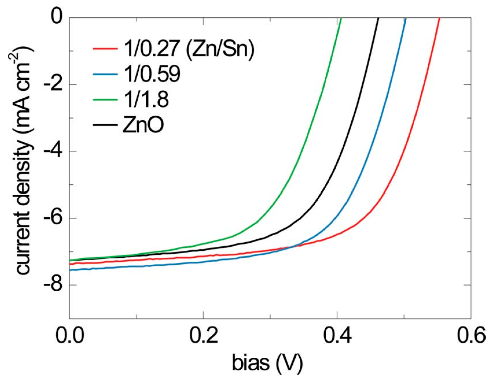
The second concerns the use of atomic layer deposition (ALD) to control the interface quality of Cu
2O heterojunction soloar cells. In a study by Lee
et al. [
35], an ultra thin buffer layer of amorphous zinc tin oxide (a-ZTO) was deposited by ALD onto electrochemically deposited Cu
2O. a-ZTO reduces recombination at the interface by acting as an electron blocking layer. The
J-V characteristics for three ZnO:Al/a-ZTS/Cu
2O/Au devices with different Zn:Sn cationic ratios in a-ZTS is shown in
Figure 6. At optimized composition of a-ZTO, an η of 2.65% was measured for these devices which is higher than the control device without a-ZTO. In a subsequent study [
36], it was further demonstrated that the ALD reaction conditions can be used to control the oxidation state of Cu and prevent the formation of an undesirable CuO interfacial layer. When the ALD temperature of the a-ZTO layer was decreased, the
Voc of ZnO:Al/a-ZTS/Cu
2O/Au devices increased, indicating reduced defects at the a-ZTS/Cu
2O interface. The highest η of 3.06% was observed at a deposition temperature of 70 °C. This group also demonstrated that insertion of 20 nm thick extrinsic Cu
2O:N between the Cu
2O and Au layers can effectively reduce contact resistance of this device structure and improve FF. This is because Cu
2O:N acts as a p-type transport layer and facilitates hole transport by tunneling [
37]. It should be noted that Cu
2O films have also been used as hole transport layers in perovskite solar cells [
38].
4. CuO Thin Film Heterojunction Solar Cells
Relatively little is known about the material properties of CuO. CuO has a monoclinic crystal structure. It has a direct energy band gap of ~1.5 eV and the absorption coefficient is also high [
1]. Since for a single p-n junction solar cell, the optimum band gap is 1.4 eV, the optical properties of CuO make it a very suitable semiconductor absorber material for solar cell applications [
11]. In addition, the electrical properties of CuO such as majority carrier mobility and minority carrier diffusion length are also adequate.
Although the narrower band gap of CuO is a better match to the solar spectrum compared with Cu
2O, little research on CuO heterojunction solar cells has been published until recently [
39,
40,
41,
42,
43,
44]. The structure of the CuO heterojunction solar cells reported so far typically involves deposition of the CuO thin films onto a semiconductor substrate such as crystalline Si wafers (
Figure 3b). The thermal oxidation method widely used for Cu
2O devices has not been used. In 2012, Gao
et al. reported a p-CuO/n-Si heterojunction solar cell fabricated by the reactive magnetron sputtering technique [
39]. The CuO layer was deposited by using a Cu target and a sputtering plasma consisting of Ar and O
2. When the flow rate ratio of O
2 to Ar was optimized, the deposited CuO has a nanocrystalline structure with a crystallite size of ~8 nm [
39]. The optical band gap of the CuO layer was 1.07 eV and the hole mobility deduced from Hall measurements was ~0.15 cm
2/V∙s [
39]. Under AM 1.5G illumination, the current density voltage (
J-V) characteristic showed a modest photovoltaic effect and an η of 0.41% was measured for a Cu/p-CuO/n-Si/Al device structure [
39]. Both
Voc and FF were low because the high series resistance of the nanocrystalline CuO layer and defects at the p-CuO/n-Si interface resulted in carrier recombination. The very thin CuO layer (100 nm) and the Cu grid top electrode might have also limited the amount of light absorbed by this device structure.
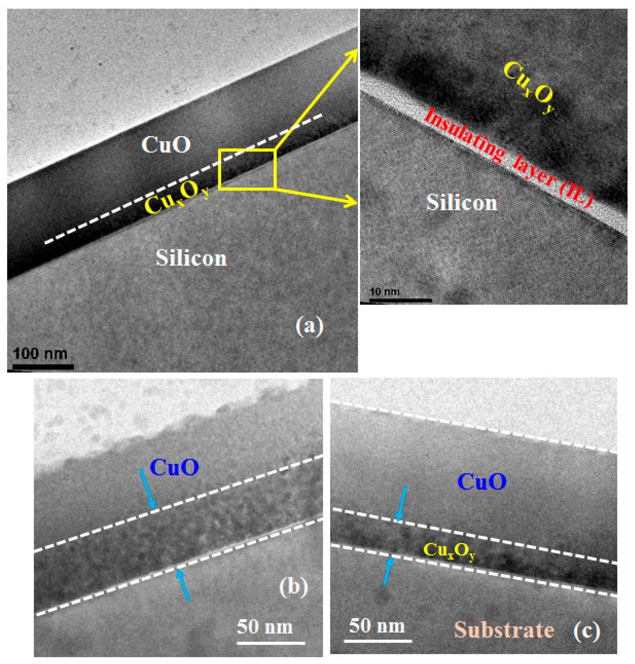
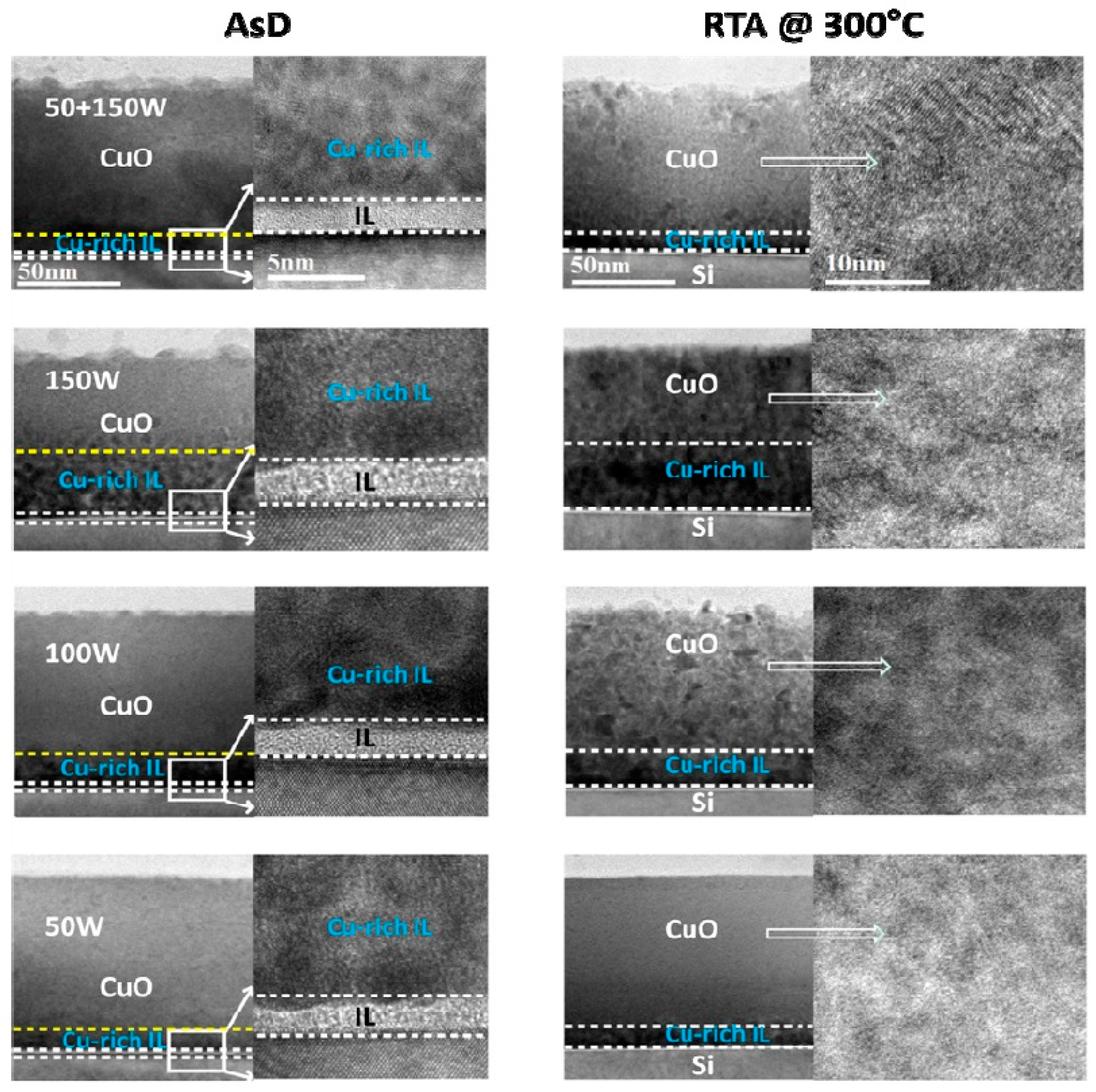
Another early study of the CuO/Si heterojunction is that by Kumar
et al. [
40]. These investigators used the RF argon sputtering of a CuO target to deposit CuO onto n-Si(100). After deposition, the polycrystalline CuO films were annealed in nitrogen at 300 °C. The crystalline structure of the film was determined by X-ray diffraction to be predominantly CuO phase for an annealing temperature of 300 °C [
40]. Under dark conditions, the CuO/Si heterojunction showed a rectifying
J-V characteristic with a rectification ratio of 10
4 (at +3 V and −3 V) [
40]. When illuminated, a photovoltage response was observed [
40]. It is also worth noting that there is a presence of interfacial oxide layer between the silicon substrate and p-CuO layer. High resolution transmission electron microscope (HRTEM) analysis reveals that the thickness of the interfacial layer is around 4 nm. Furthermore, a Cu-rich interfacial layer between p-CuO and silicon substrate is also observed and the Cu-rich interface layer significantly depends on the sputtering power, as shown in
Figure 7.
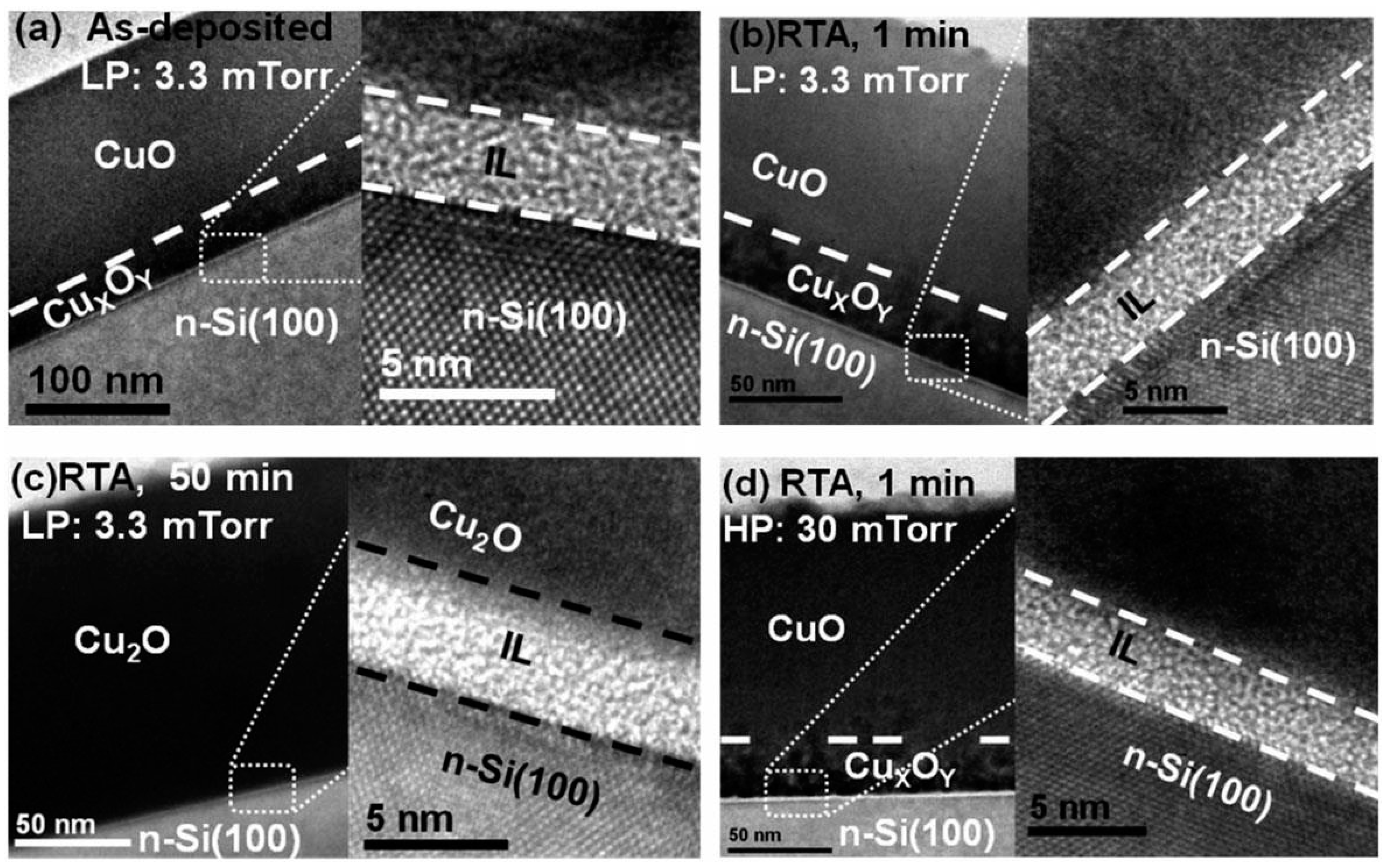
A CuO heterojunction solar cell with PCE approaching 1% was reported recently by Masudy-Panah
et al. [
41]. The heterostructure studied was Al/Ti/n-Si/p-CuO/Ti/Al. The CuO layer was deposited by argon RF sputtering of a CuO target at a fixed power of 150 W and working pressure in the range of 3 to 35 mTorr. After deposition, the CuO film was further annealed at 300 °C from 1 min to 1 h. The CuO film properties are influenced strongly by both the working pressure and annealing time. By using X-ray diffraction and Raman spectroscopy, the CuO phase was found to have improved crystallinity when a higher working pressure was used. In addition, when annealed for a prolonged period, there is a phase transformation from CuO to Cu
2O and a mixture of CuO and Cu
2O was formed as a result. This phase transformation is corroborated by X-ray photoelectron spectroscopy analysis. The position of the Cu 2p peak shifted from 934.0 eV to 932.4 eV [
41]. In the Raman spectrum, the formation of Cu
2O is signified by the appearance of peaks between 119 cm
−1 and 500 cm
−1. In addition, a peak at 1110 cm
−1 indicates that elemental Cu is present in the CuO as a Cu rich copper oxide. This Cu rich copper oxide within the CuO was observed by HRTEM to be about ~30 nm thick for a CuO film thickness of 150 nm, as shown in
Figure 8 [
41]. In between the Cu rich copper oxide and the Si substrate is an amorphous interfacial layer (IL) due to residual oxygen in the sputtering system. Its composition was found by energy dispersive X-ray (EDX) spectroscopy to be comprised of Si, Cu and O [
41].
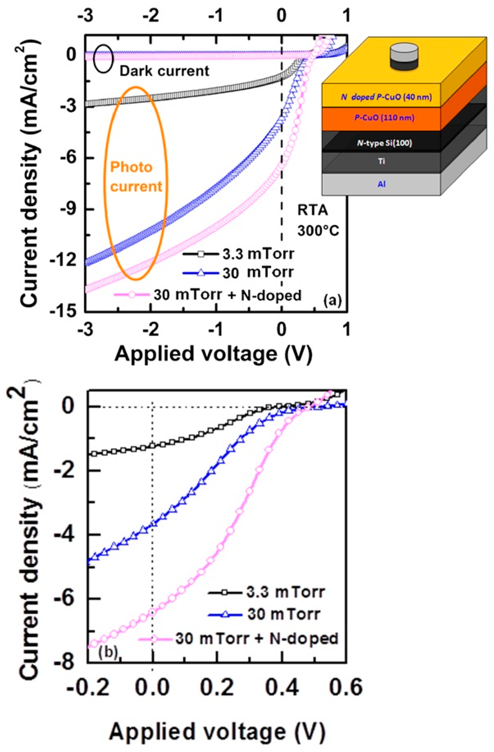
Both the Cu rich copper oxide and the amorphous IL are detrimental to interface quality and thus need to be minimized by controlling the sputtering conditions of the CuO. This was demonstrated by photocurrent voltage characteristics of Al/Ti/p-CuO/n-Si/Ti/Al devices. The
Voc of devices with CuO deposited at low working pressure and annealed at 300 °C for 1 min was 380 mV and the η was only 0.14% [
41]. When the annealing time was increased, the
Voc decreased further due to the thickening of the IL and the Cu rich copper oxide layer. On the other hand, the
Voc of the device increased to 509 mV when the CuO layer was deposited at 30 mTorr and annealed at 300 °C for 1 min [
41]. This improvement in
Voc is due to thinner interfacial layers and better CuO crystallinity. As a result, a higher η of 0.36% was obtained. This study shows that the CuO deposition and annealing conditions play a crucial role in determining the achievable photovoltaic performance of p-CuO/n-Si heterojunction solar cells. Furthermore, through the introduction of highly nitrogen doped CuO thin film in between CuO layer and top metal contact, the fill factor of the device improved significantly and, as a result, efficiency of the device increased to 1%, as shown in
Figure 9.
Since the poor photovoltaic performance of p-CuO/n-Si heterojunction solar cells was attributed to native oxide formation and a Cu rich IL during the sputtering process, a comprehensive study on the IL properties was carried out by Masudy-Panah
et al. [
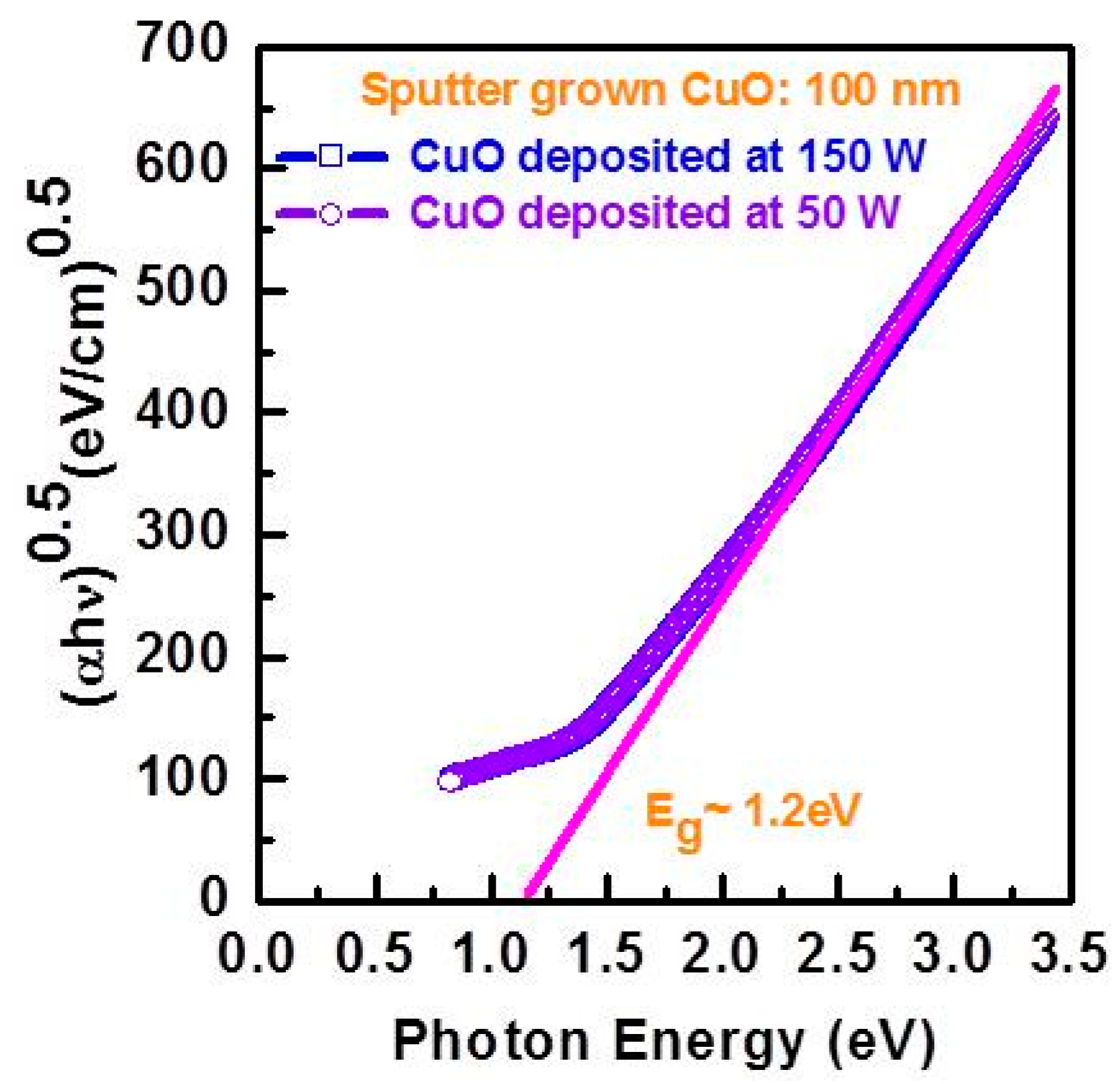
42]. CuO films were deposited at different RF power (50 W, 100 W and 150 W) onto Si using a stoichiometric CuO target. The composition profile, crystallinity and the structure of the CuO/Si interface was studied by time of flight secondary ion mass spectrometry (TOF-SIMS), Raman spectroscopy, TEM and X-ray diffraction respectively. For an RF power of 50 W, the composition of the CuO layer was quite uniform. When the RF power was increased to 150 W, the Cu rich IL became thicker and the crystalline quality of the CuO improved without compromising the optical band gap of the thin film CuO determined from the Tauc plot of the absorption coefficient
α and photon energy
hν (
Figure 10). This finding leads to a two-step sputtering process in which a thin layer of CuO is first sputtered at low power (
i.e., 50 W) followed by a thicker layer of CuO deposited at 150 W. The resulting CuO can have both good crystallinity and a thin Cu rich IL (
Figure 11). In order to demonstrate the improved film properties for the two step process, the photovoltaic performances of several p-CuO/n-Si devices were compared for one-step and two-step deposition of CuO. For the one-step process, the lowest RF power (50 W) led to the highest η of 0.38%. At higher RF power, the increased thickness of the Cu IL alluded to above led to a loss of efficiency. When the two-step process is used instead with the CuO layer deposited at higher power and doped with nitrogen, an η of 1.21% was obtained. This is the first report of a CuO heterojunction solar cell with an η above 1% [
42].
Since high sheet resistance and low carrier concentration of a CuO absorber layer are possible reasons of poor photovoltaic performance of copper oxide solar cells, a detailed study on doping of CuO thin films was carried out by Masudy-Panah
et al. [
43,
44]. These investigators report that the impact of nitrogen doping on the crystal quality of CuO thin films significantly depends on its concentration and annealing temperature [
43]. Thermal treatment of lightly doped samples with N concentration of 1.5% did not cause significant changes in its crystal structure regardless of annealing temperature. However, CuO-Cu
2O mixed phase was formed for the highly doped samples annealed at low temperatures and a dominant Cu
2O phase was formed for the highly doped samples annealed at high temperatures.
The reflectance and transmittance of N-doped CuO thin films in the wavelength range of 200 nm–1500 nm was found to be increased with increasing nitrogen concentration. It was explained by Masudy-Panah in terms of CuO bandgap widening and the presence of Cu
2O phase. It was also shown that by tuning the nitrogen concentration during sputter growth of CuO film (
in situ nitrogen doped), the color of the copper oxide film can be tuned for as-deposited and also for the annealed films as shown in
Figure 12.
Impact of N-doping on photovoltaic properties of p-CuO(N)/n-Si based heterojunction solar cells was also studied [
43].
Voc of doped samples was found to degrade with increasing N doping concentration. According to the investigators, nitridation of Cu-rich interfacial layer and formation of poor quality copper oxide nitride/Si interface could be the reasons of the
Voc degradation. Photovoltaic properties of highly doped samples were found to be significantly lower because of CuO bandgap widening and Cu
2O formation despite of lower sheet resistance. However, lightly doped samples showed better photovoltaic performance over highly doped samples and control samples. Improvements in
Jsc,
FF and η were attributed to the reduction of series resistance of N-doped CuO thin films.
In another study, Masudy-Panah
et al. showed that, by Ti-doping, it is possible to significantly reduce resistivity of CuO thin films while maintaining its optical properties and structural quality [
44]. The crystal structure of Ti-doped CuO thin films maintained good quality when Ti concentration was increased up to 0.099%. Doping with higher Ti concentrations resulted in formation of secondary defect phases which decreased crystalline ordering. The transmittance and reflectance of Ti-doped CuO were found to be independent of Ti dopant concentration. Furthermore, Ti doping has insignificant impact on surface morphology of CuO films.
The p-CuO(Ti)/n-Si heterojunction solar cells with Ti concentration of 0.099% showed better performance over undoped samples and other Ti-doped samples. Both Voc and Jsc improved in comparison with control samples and other Ti-doped samples. Masudy-Panah et al. explained these improvements by reducing of series resistance and enhancing of collection efficiency. When the two-step process was used instead to deposit the Ti-doped CuO absorber layer at high working pressure of 30 mTorr, an η of 1.2% was obtained. However, overall performance of highly doped samples significantly reduced because of high recombination rate with CuO layer.
Dalapati
et al. reported that CuO thin films deposited by RF magnetron sputtering at high working pressure of 30 mTorr have better crystal quality than the films deposited at lower working pressure of 3.3 mTorr while optical properties remain the same [
45]. Investigators showed that CuO thin films grown at high working pressure exhibit lower defect density and higher carrier concentration.
In the CuO devices discussed thus far, the sputtered CuO layer is always p-type. Recently, however, Lee
et al. has observed n-type behavior in nanoscale non-stoichiometric CuO
x deposited by reactive magnetron sputtering [
46]. The n-type conductivity which was confirmed by Hall effect measurements results from the fact that in the initial stage of deposition, the CuO
x is Cu rich and this causes electrons to be majority carriers. By depositing 50 nm of n-CuO
x onto intrinsic i-a-Si:H in a heterojunction p-i-n device structure, a maximum η of 3.04% was measured [
46]. This can be further increased to 4.79% by inserting a thin n-mc Si:H depletion assisting layer (DAL) between the CuO
x and i-a-Si:H layer. The DAL enhances η of the device by increasing
Voc.
The performance of CuO heterojunction solar cells can be further enhanced by the use of mixed phase copper oxide nanopowders (NP). This innovative approach to boost light absorption was demonstrated by Bhaumik
et al. in 2014 [
20]. The device structure studied consists of glass/ITO/ZnO/CuO/NP(Cu
2O, CuO) (
Figure 3c). This structure is different from all the device structures discussed thus far because sunlight is incident from the transparent substrate rather than from the top of the device. In addition, both ZnO and CuO layers were deposited by PLD from the respective targets using a krypton fluoride (KrF) excimer laser to minimize the defect density at the interface. The mixed phase NP containing both cupric oxide and cuprous oxide was synthesized from CuSO
4 and KOH by a hydrothermal process within a sealed autoclave at 80 °C. After synthesis, the mixed phase NP dispersed in toluene was drop cast onto the surface of the CuO thin film and annealed in oxygen for up to two hours. For the device annealed in this manner for two hours, the
Jsc under AM1.5 solar illumination was 20.9 mA/cm
2 [
20]. This is much higher than the
Jsc of the control device with only the thin film layers (290 μA/cm
2) and another device with commercial copper oxide micro-powder (4.22 mA/cm
2). Interestingly, the
Voc of the device was also improved by the NP and annealing. After annealing for 2 h, the
Voc increased from 0.3 V to 0.4 V. As a result, a high η of 2.88% was achieved. This is the highest reported efficiency for a CuO heterostructure solar device. The high performance was explained in terms of: (i) increased light absorption caused by the copper oxide NP; and (ii) improved diffusion of electrons and holes due to removal of ligands from the NP after annealing. As for
Voc, the increase was attributed to the increase in band gap and improved band alignment for the copper oxide layer.
Another copper oxide nanostructure is the nanoleaf (NL). CuO NL can be solution synthesized by a two-step process on crystalline Si subtrates. In [
47], CuO NLs were grown on commercial surface textured n
+-p Si solar cells without passivation layer. After growth, the NLs have an average length of ~280 nm and width of ~83 nm (
Figure 13). The NL layer enhances light absorption in the Si solar cell by acting as a graded index layer, which increases light scattering and trapping across a broad spectral region. In addition, the small CuO/n
+Si heterojunction beneath each NL facilitates charge extraction from the device. When the morphology of the NL is optimized, the η of CuO NL/n
+-p Si solar cell can reach 11.07%, which is significantly higher than the control device (9.39%) [
47]. Very recently, CuO nanoparticles prepared by green synthesis have also been used as counter electrodes of dye sensitized solar cells [
48].
In recent years, the photovoltaic behavior of CuO/fullerene (C
60) heterojunctions has also been investigated. This inorganic-organic heterojunction structure is motivated by the fact that CuO is a p-type material while fullerene is an n-type (acceptor) material used for both heterojunction and bulk heterojunction organic solar cells. Oku
et al. used electrochemical deposition to deposit CuO onto ITO working electrode by using an aqueous electrolyte consisting of CuSO
4 and 1-lactic acid at 65 °C [
49]. The C
60 powder and top Al electrode were deposited on to CuO by vacuum evaporation. The measured η of the device, however, was extremely low (~10
−4%) due to low
Voc, FF and
Jsc.
In summary, the key developments in CuO devices are the RF sputter deposition of both p-type CuO and n-type CuOx. Both oxides form heterojunctions with Si, but DAL is needed for CuOx and control of the interfacial layer is critical. The performance of CuO devices can be enhanced by the incorporation of CuO NP and NL to enhance light absorption.


