1. Introduction
Escalating industrialization has exacerbated air pollution, posing significant threats to both the environment and human health. Consequently, the effective monitoring and control of gaseous pollutants such as CO, NO, NO
2, NH
3, and SO
2 have become critical. Gas sensors are indispensable for this purpose, with vital applications in industrial safety, public air quality monitoring, and emission control systems [
1].
A key area of application is the automotive sector, where stringent regulations like the European Union’s Euro standards mandate the reduction in harmful vehicle emissions. Selective Catalytic Reduction (SCR) systems in diesel engines are the primary technology for neutralizing nitrogen oxides (NO
x) [
2]. An SCR system’s efficiency relies critically on a fast and accurate NO
2 sensor. This sensor provides real-time data to the engine control unit (ECU), which then precisely meters a urea-based solution (AdBlue) into the exhaust stream. This process catalytically converts toxic NO
x into harmless nitrogen (N
2) and water (H
2O) [
3]. Therefore, the sensor’s performance is paramount for maximizing emission reduction while preventing operational issues like ammonia slip [
4].
However, conventional sensor technologies face significant limitations. Traditional thick-film sensors often lack the required sensitivity and response time, while some thin-film alternatives can suffer from long-term stability issues [
5]. These drawbacks have spurred research into alternative materials. Perovskite-type oxides are particularly promising candidates, offering excellent thermal stability and tunable electrical properties suitable for high-performance gas sensing [
6]. Perovskites incorporating transition metals such as manganese (Mn), cobalt (Co), or iron (Fe) are exceptionally promising due to their versatile electronic structures and catalytic activity [
7].
A critical aspect of this research is the use of advanced ablative deposition techniques to synthesize thin film sensors. While traditional methods like Chemical Vapor Deposition (CVD) and sputtering are industry standards, they are associated with significant environmental drawbacks. These techniques often rely on hazardous chemical precursors and carrier gases, leading to toxic waste generation. In contrast, ablative techniques, such as Pulsed Electron Deposition (PED), offer a more sustainable and efficient pathway for producing high-quality thin films [
8]. As a physical deposition method, PED eliminates the reliance on toxic and volatile chemicals, minimizing hazardous byproduct generation. It also provides exceptional control over film thickness, crystallinity, and microstructure at lower substrate temperatures, leading to improved device performance and reduced energy consumption [
9].
A cornerstone of this work is the strategic doping of the perovskites with strontium (Sr). Substituting lanthanum (La
3+) with strontium (Sr
2+) in lanthanum cobaltite (LaCoO
3) induces charge-compensating defects, such as oxygen vacancies and changes in the oxidation state of the B-site cations (Co). These modifications are paramount for enhancing gas sensing performance, as oxygen vacancies create more active sites for gas adsorption and dissociation. This defect engineering approach is crucial for developing highly sensitive and selective resistive sensors [
10]. By combining the tailored properties of Sr-doped perovskites with the environmental and practical benefits of ablative fabrication, this research aims to advance the development of next-generation thin-film sensors.
2. Research Material
Lanthanum cobaltite (LaCoO
3) perovskite oxide is a highly promising material for catalytic applications due to its unique combination of electronic, magnetic, and structural properties. A key advantage is its remarkable mixed ionic and electronic conductivity, which is crucial for processes requiring efficient charge transfer and oxygen mobility, such as in solid oxide fuel cell (SOFC) cathodes, oxygen separation membranes, and catalysts for CO oxidation [
11].
Structurally, LaCoO
3 is exceptionally stable, maintaining its rhombohedral (R3c) or orthorhombic (Pbnm) crystal structure up to a high melting point of 1740 °C. The material’s properties can be precisely tailored by inducing structural distortions through temperature changes or cation substitution at the B-site. A defining catalytic characteristic of LaCoO
3 is the tunable spin state of its cobalt ions, a feature rarely observed in other magnetic oxides [
12]. Materials’ electronic behavior is governed by the presence of mixed Co
3+/Co
4+ valence states. Below 100 K, Co
3+ ions adopt a low-spin state. With increasing temperature, they undergo a gradual transition to intermediate- and high-spin states. This spin-state transition, which can also be influenced by external gas pressure, directly modulates the electronic structure by altering interatomic distances and bond angles, thereby influencing the material’s magnetic and catalytic activity [
13,
14].
The conductivity mechanism in LaCoO
3 is highly temperature-dependent. Between 110 K and 350 K, its semiconducting behavior is governed by a small-polaron hopping mechanism. Above 650 K, the material undergoes a semiconductor-to-metal transition, leading to a significant increase in p-type electronic conductivity. This transition is associated with the stabilization of high-spin cobalt ions, which creates a partially filled electron shell that facilitates excellent charge transport [
15].
Crucially for catalysis, the material’s ionic conductivity—driven by the diffusion of oxygen ions through lattice vacancies—is also enhanced at elevated temperatures. This synergy between high electronic and ionic conductivity is a major advantage for catalytic processes that depend on both electron transfer and oxygen activation. This unique combination of high thermal stability, tunable electronic structure, and excellent mixed conductivity makes LaCoO
3 a versatile and highly effective catalyst, with demonstrated potential in applications ranging from SOFCs to low-temperature CO detection [
16].
Building upon the preceding discussion of their gas-sensing properties, this study focuses on the fabrication and comprehensive analysis of La(Sr)CoO3 perovskite thin films, examining their structure and catalytic activity. The selection of a suitable deposition technique is paramount for producing high-quality functional films. Pulsed Electron Deposition (PED) presents a highly advantageous solution, primarily due to its unique capability for stoichiometric transfer. This process effectively preserves the phase and chemical composition of the target material in the resulting nanocrystalline film, crucially avoiding gas-phase decomposition. Nevertheless, successful deposition is contingent upon the meticulous selection of the substrate and the precise optimization of key process parameters. This paper elucidates these critical factors, providing a methodological framework for depositing high-quality perovskite thin films via the PED technique.
3. Methodology and Research Techniques
3.1. Target Fabrication for PED Process
This study’s initial phase focused on the fabrication of perovskite targets for subsequent Pulsed Electron Deposition (PED). The targets were derived from nanopowders synthesized through a mechanical alloying route using high-purity La
2O
3, Co
3O
4, and SrO as base materials. The starting materials for target fabrication via mechanical synthesis were sourced from a reputable global supplier (Kurt J. Lesker, Sigma-Aldrich/Merck, St. Louis, MO, USA). The quality of all powders was verified before use. As per the manufacturer’s specifications, the materials met the required purity and particle size: Lanthanum(III) oxide (La
2O
3, 99.99% trace metals basis), Cobalt(II,III) oxide (Co
3O
4, nanopowder, <50 nm, 99.5% trace metals basis), and Strontium oxide (SrO, 99.9% trace metals basis). Prior to synthesis, these powders were calcined to remove residual moisture, thereby ensuring the formation of the correct perovskite phase with the intended stoichiometry. The high-energy milling process was carried out in a planetary ball mill Retsch PM 100 (Retsch GmbH, Retsch-Allee 1-5, 42781 Haan, Germany) for a total duration of 28 to 30 h at a rotational speed of 550 to 650 RPM, employing cycles of 2-h milling and 30-min rests. Three distinct perovskite materials were successfully synthesized: stoichiometric LaCoO
3, alongside two Sr-doped compositions, La
0.9Sr
0.1CoO
3 and La
0.8Sr
0.2CoO
3. The procedure for preparing targets for the electron ablation process is identical to that for preparing materials for the laser ablation process mentioned in the previous summary [
17].
3.2. Perovskite Thin Film Deposition
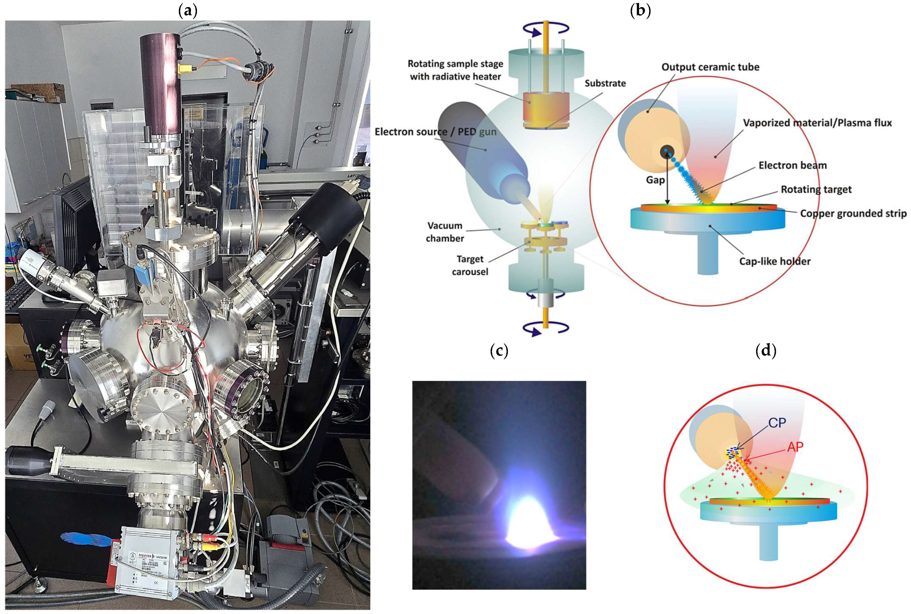
Pulsed Electron Deposition (PED) technique utilizes a high-energy, pulsed electron beam to vaporize (ablate) material from a target. The ablated material subsequently condenses onto a substrate, forming a coating/film. Due to its unique properties, PED is an attractive alternative to the more widespread method of Pulsed Laser Deposition (PLD). The mechanism of deposition is as follows: a short (approx. 100 ns), intense, high-energy (10–20 keV) electron pulse is generated in an electron source (gun). This pulse strikes the target’s surface, causing its rapid and nearly instantaneous heating and evaporation (
Figure 1b,c). In contrast to laser photons, electrons penetrate the material to a finite depth, resulting in volumetric heating. A key requirement of the electron deposition technique is to ensure a uniform and stable distribution of gas pressure (concentration) in the chamber, where the target, as an integral part of the discharge circuit, affects the dynamics of electron beam generation and its parameters (
Figure 1d).
Perovskite La(Sr)CoO
3 thin films were deposited on [001]-oriented, epi-polished single-crystal Si and MgO substrates using pulsed electron deposition. The process was carried out in a Neocera PLD/PEBS 32 system (Neocera, LLC, Beltsville, MD, USA), which is equipped with a Pioneer 180 vacuum chamber and an integrated electron gun (
Figure 1a). The key deposition parameters are summarized in
Table 1.
The applied parameters successfully produced high-quality, ultra-thin films suitable for subsequent analysis. The electron beam deposition process can be further optimized by slightly reducing the per-pulse electron energy (accelerating voltage) while concurrently increasing the number of pulses to extend the deposition time. Alternatively, a similar effect can be achieved by lowering the pulse repetition rate—a technique frequently recommended for obtaining smooth films on the order of a few nanometers. While increasing the target-to-substrate distance can enhance surface quality, it is important to note that electron ablation is a highly directional process. Therefore, an excessive working distance will negatively impact the film’s homogeneity, particularly its thickness uniformity.
3.3. Research and Analytical Techniques Applied
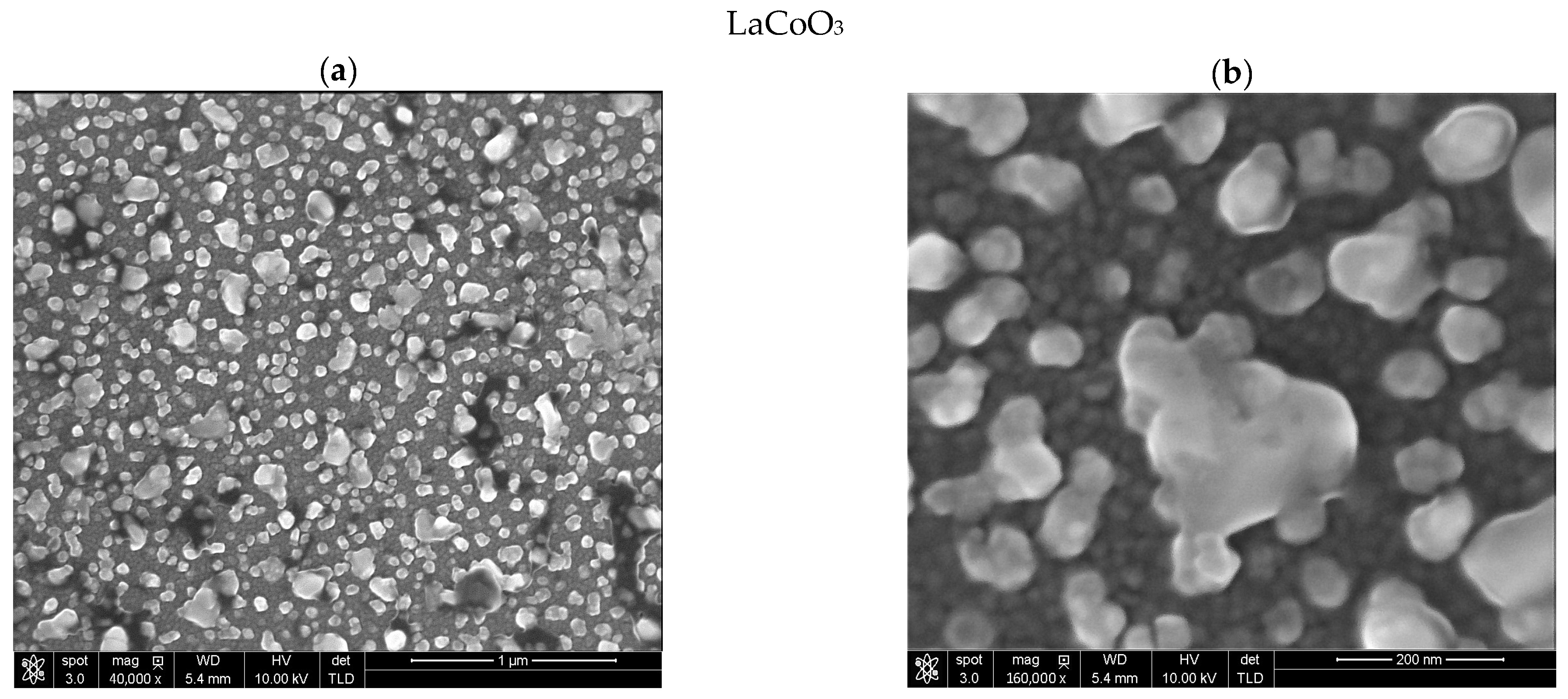
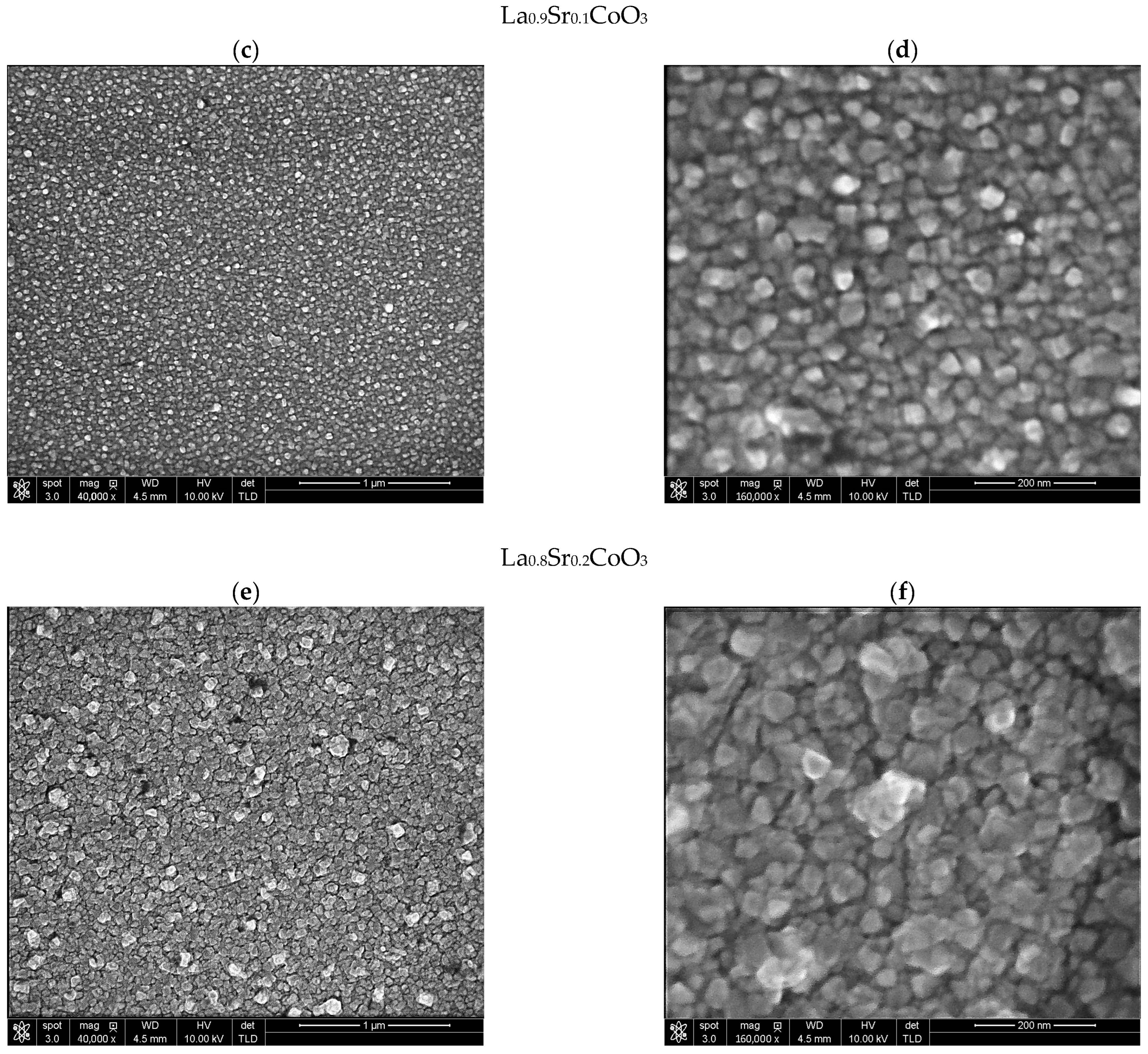
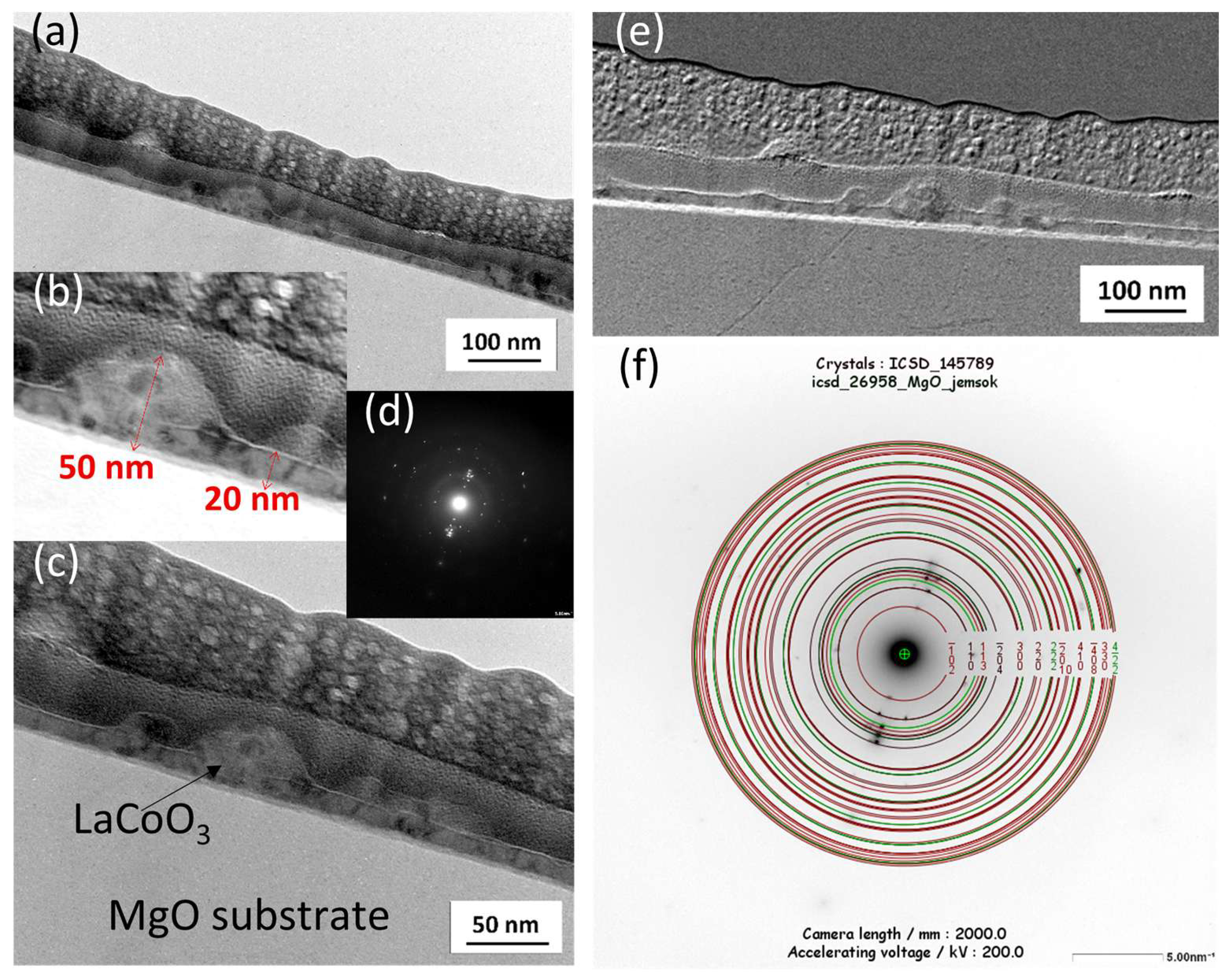
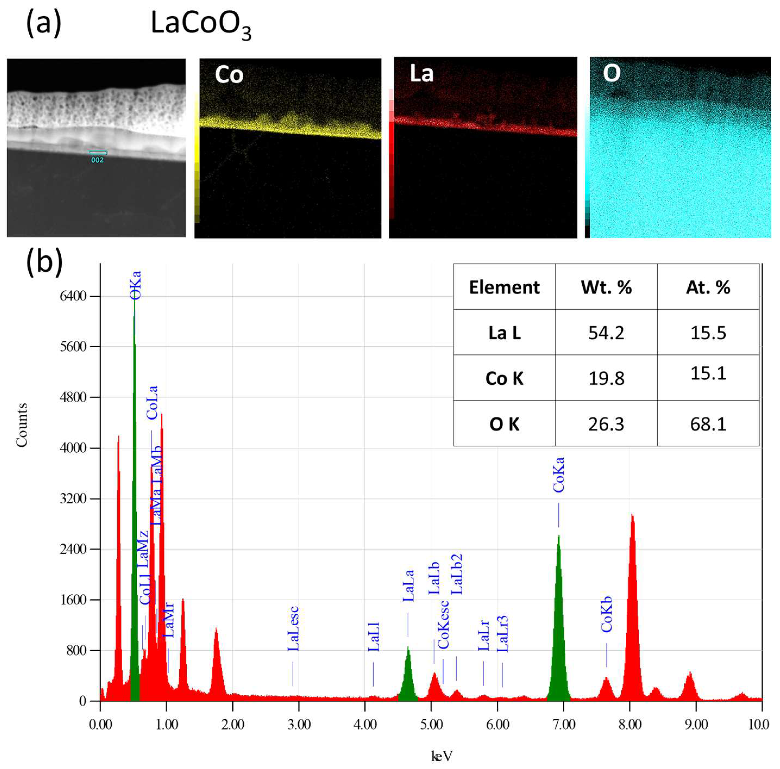
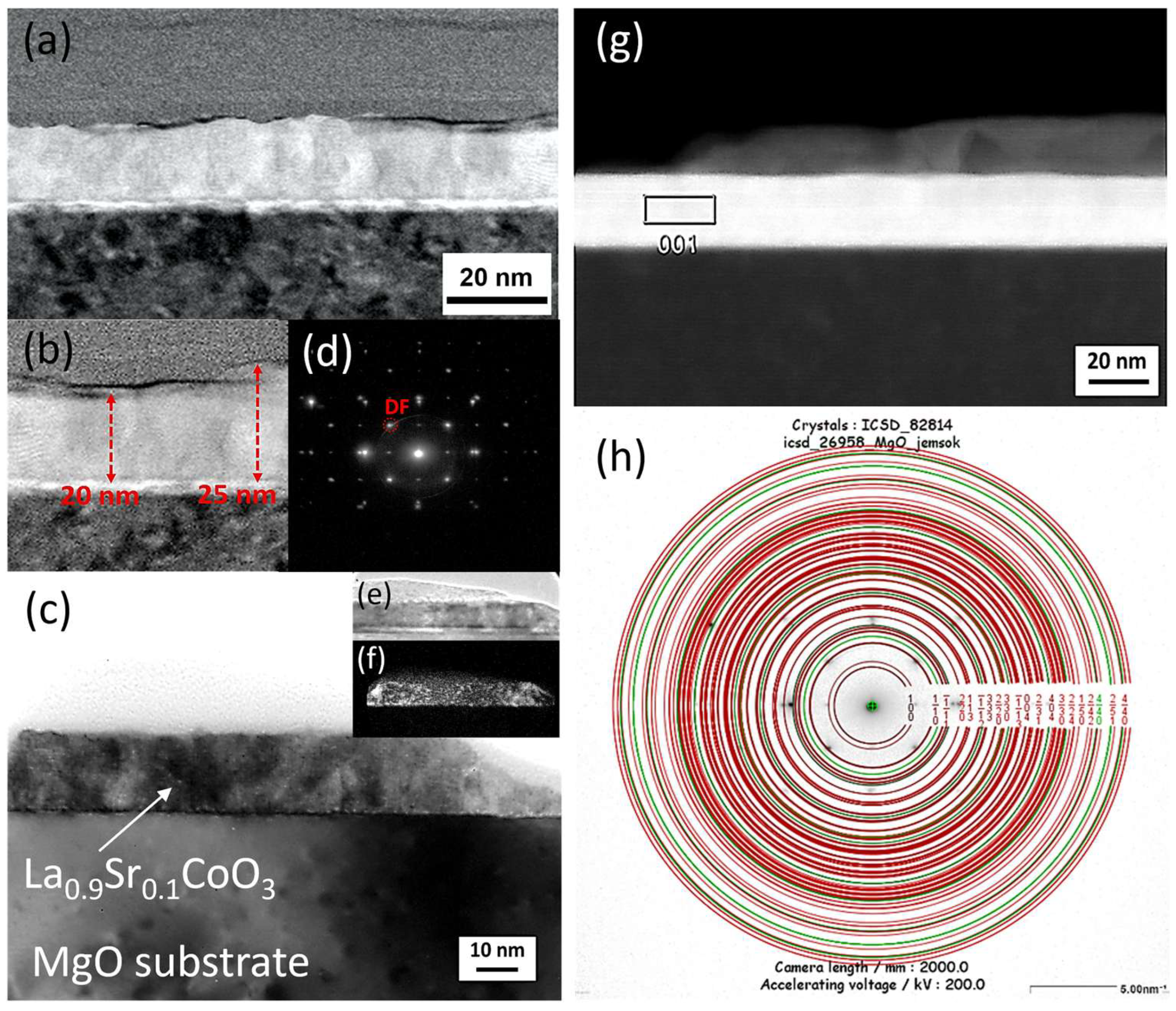
The microstructure and chemical composition of the thin films were analyzed using scanning and transmission electron microscopy. Scanning electron microscopy (SEM) was performed with a FEI Nova NanoSEM 450 system equipped with an EDAX Octane Elect Plus Energy Dispersive Spectroscopy (EDS) detector (Thermo Fisher Scientific Inc., Waltham, MA, USA). Transmission electron microscopy (TEM) analysis was conducted on a JEOL JEM-ARM200F NEOARM microscope (JEOL Ltd., Tokyo, Japan) fitted with an Oxford Instruments EDS detector (Abingdon, Oxfordshire, UK). Cross-sectional samples for TEM were prepared using a focused ion beam (FIB) milling technique.
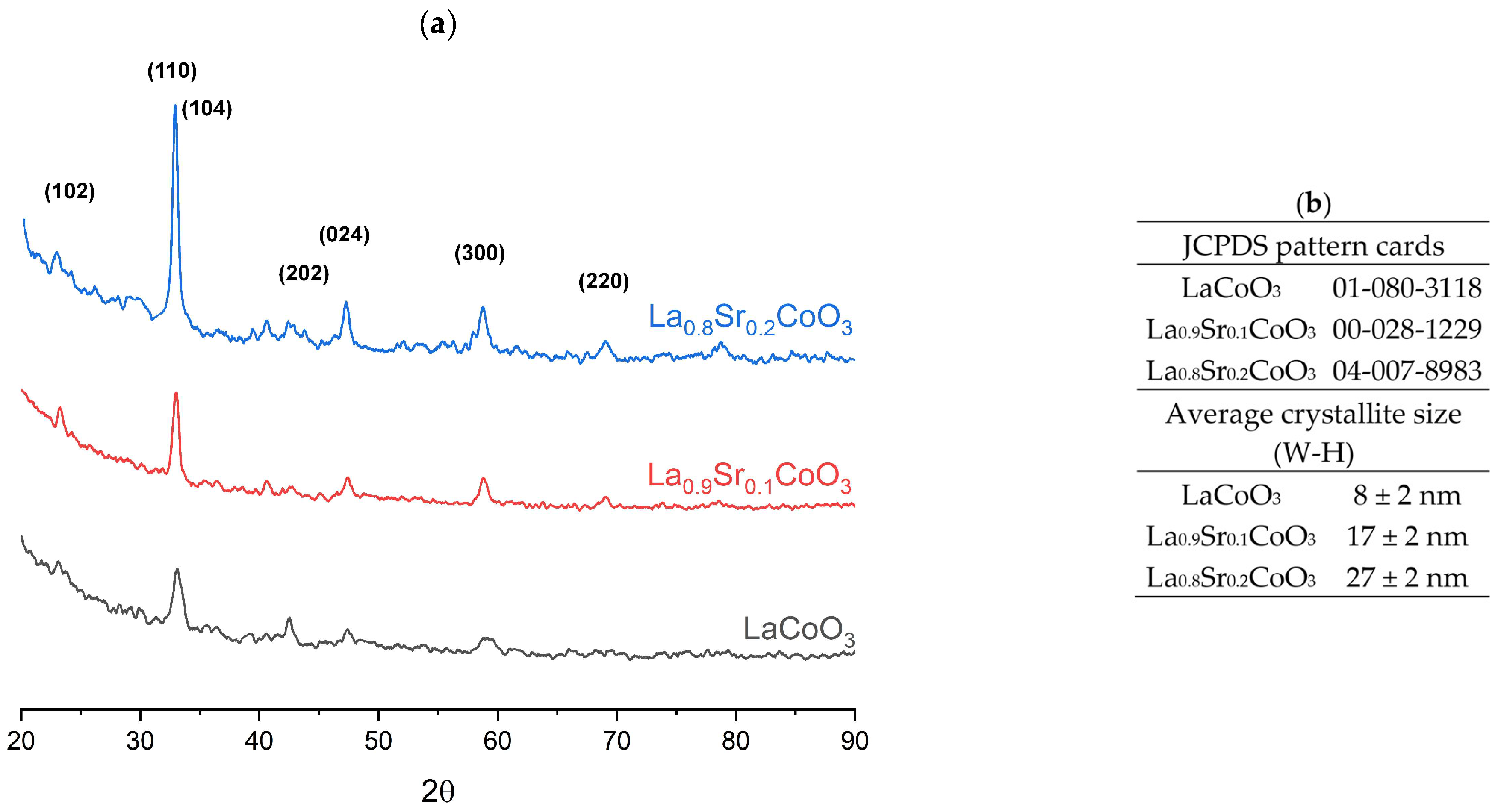
The crystalline structure of the films was investigated by X-ray diffraction (XRD) on a PANalytical EMPYREAN DY 1061 diffractometer (Malvern Panalytical Inc., Westborough, MA, USA). The analysis was performed in a grazing incidence configuration (α = 1°) using CuKα radiation (λ = 0.154 nm). The collected diffraction patterns were interpreted with PANalytical Highscore 4.9 software. Phase identification was carried out using the ICDD PDF-4+ database, while phase analysis and crystallite size determination were performed with the MAUD program (Version 2.9999; 28 May 2025).
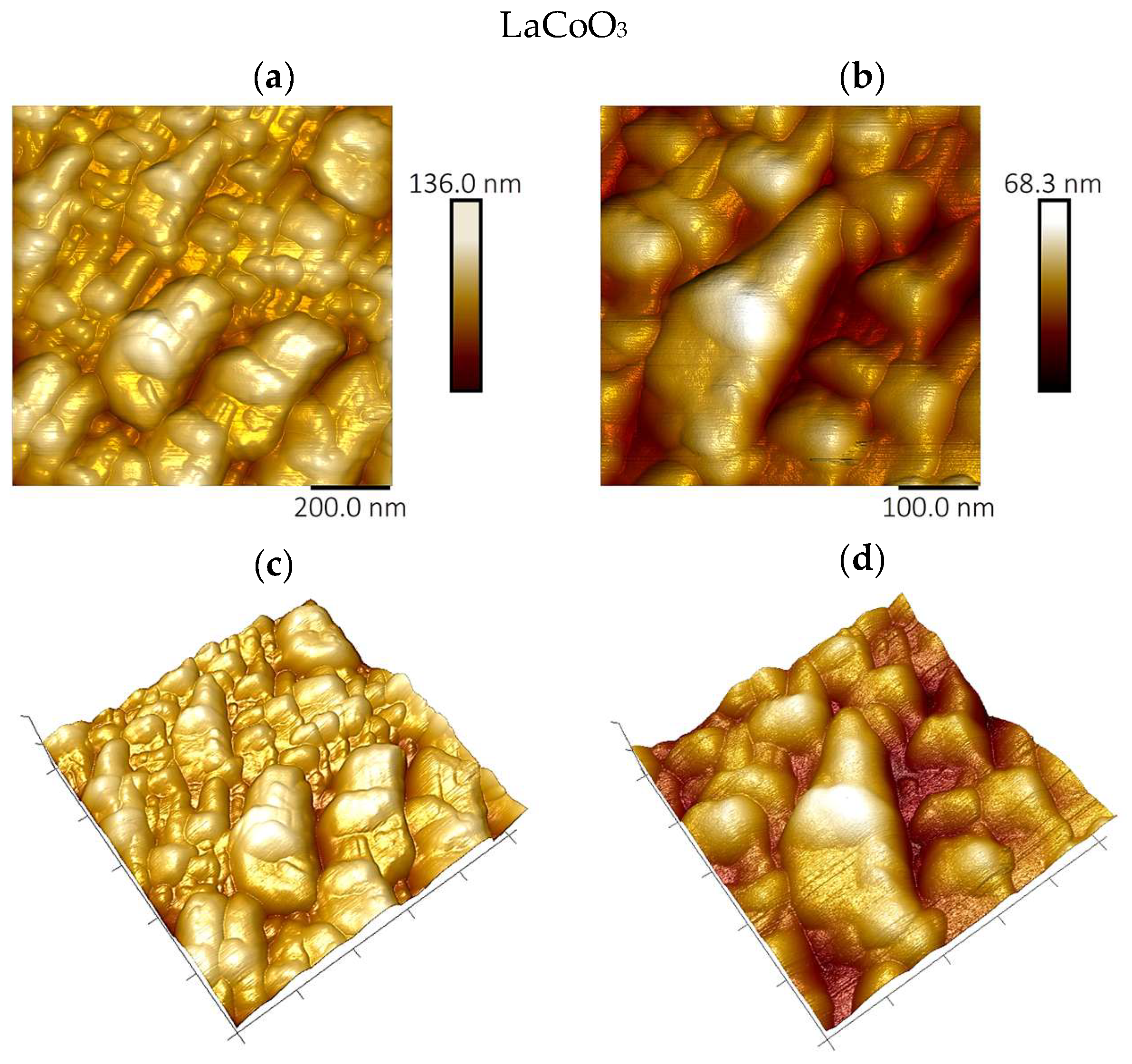
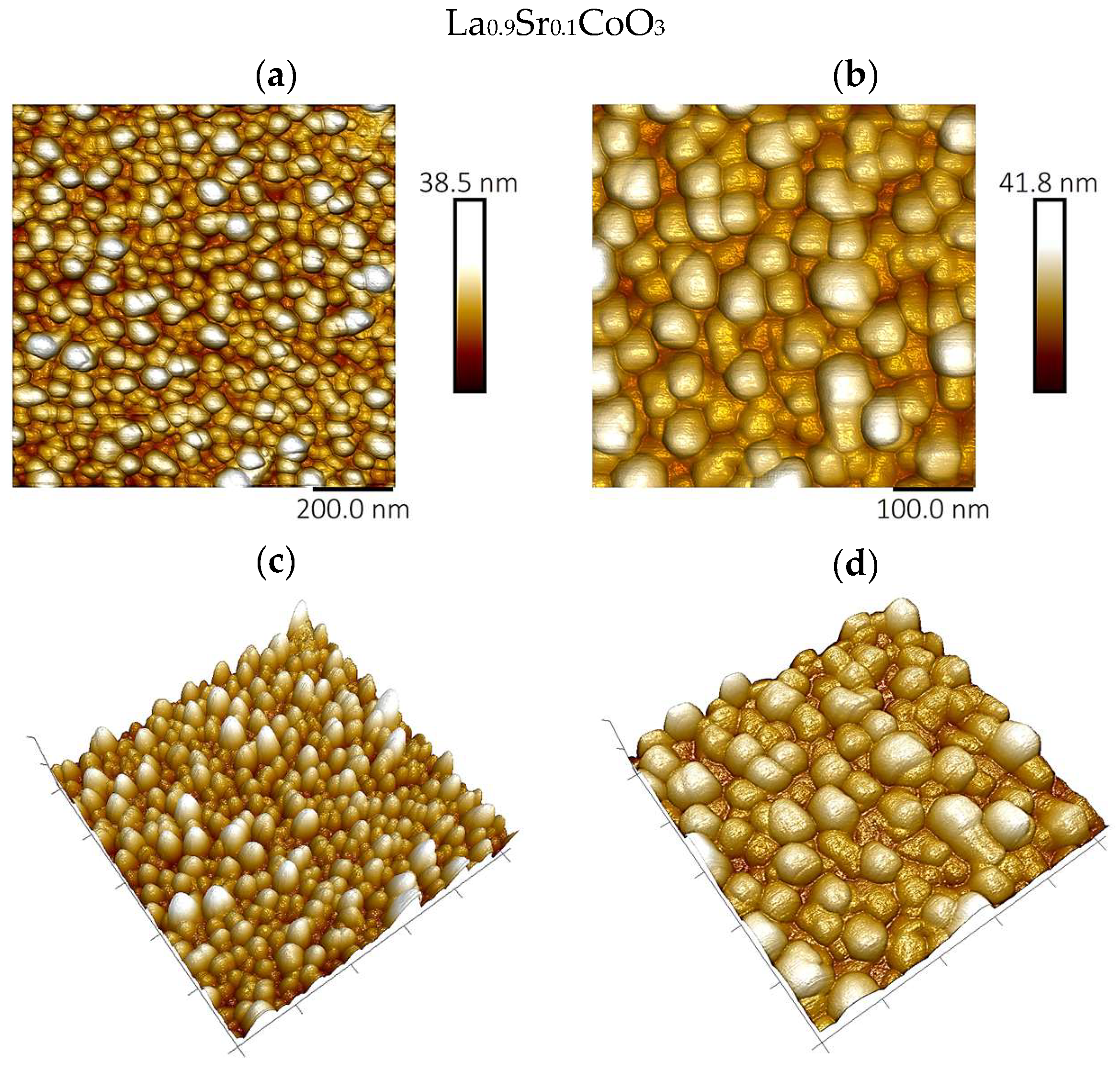
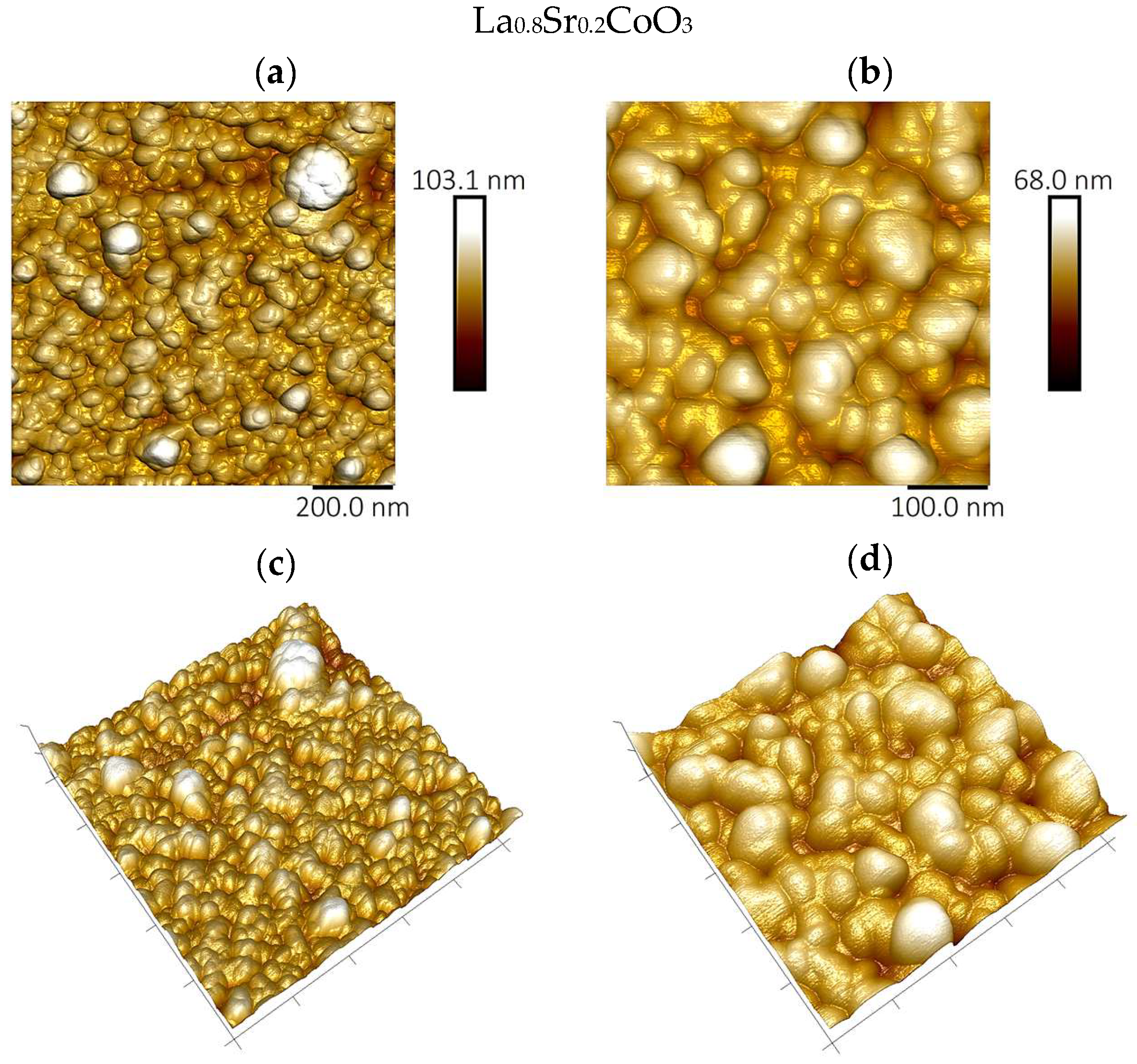
The surface topography and roughness of the deposited perovskite thin films were examined by atomic force microscopy (AFM) using a Bruker Dimension Icon instrument (Billerica, MA, USA).
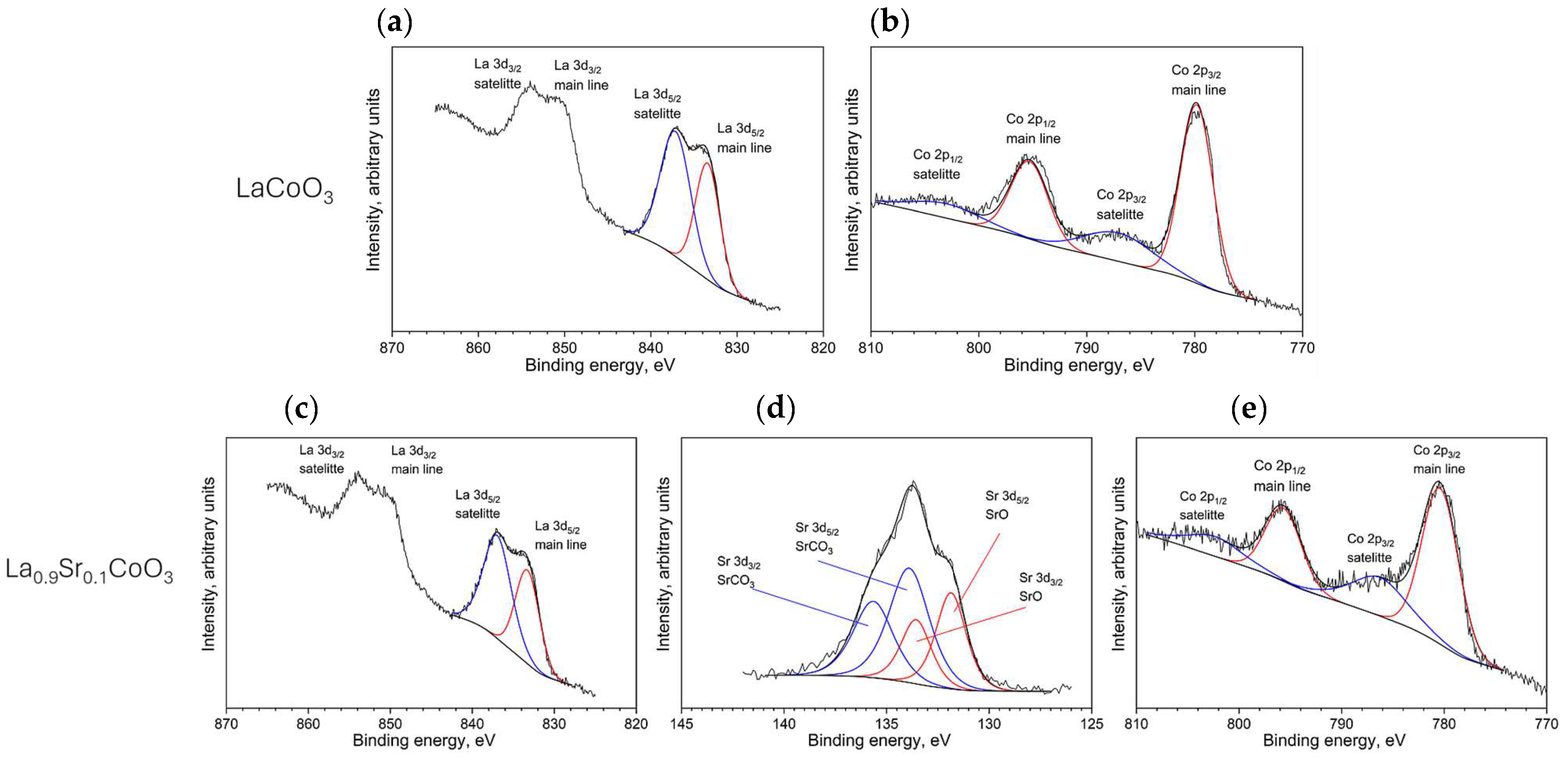
X-ray photoelectron spectroscopy (XPS) was used to analyze surface chemistry. The analyses were performed on a PHI Versa Probe II instrument (Physical Electronics, Inc., Chanhassen, MN, USA) equipped with a monochromatic AlKα X-ray source (E = 1486.6 eV). Spectra were acquired using a pass energy of 47 eV and a take-off angle of 45°. Charge neutralization was achieved with a combination of an argon ion gun and an electron flood gun. The binding energy scale was calibrated by referencing the C 1s peak of adventitious carbon to 284.8 eV.
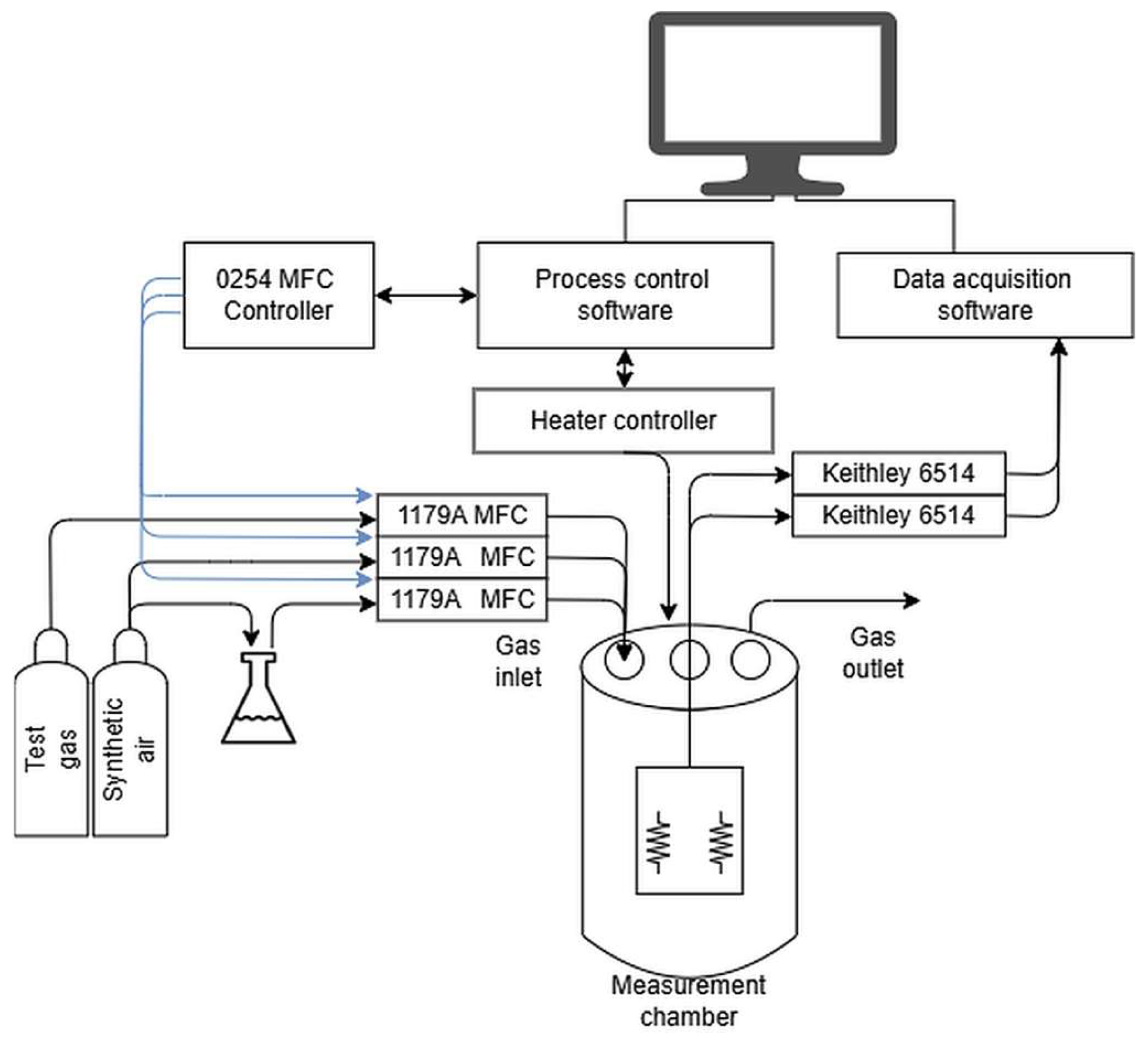
The catalytic properties measurement system was managed by a computer running dedicated control and data acquisition software GasResControl V1.2 (
Figure 2). The electrical resistance of the samples was measured using two Keithley 6514 electrometers (by Keithley Instruments, part of Tektronix, Beaverton, OR, USA), selected for their high accuracy, low noise, and broad measurement range (10 mΩ to 200 GΩ). These instruments provide precise and stable readings critical for evaluating the sensor layers under diverse gas and temperature conditions.
The sensor layers under investigation, deposited on Si substrates, were positioned on a stainless-steel stage within a quartz tube (internal volume: 100 cm3) that functions as the measurement chamber. This chamber was equipped with electrical feedthroughs for sensor connections and ports for gas inlet and outlet. Platinum wire contacts were affixed to the sample surface using a conductive silver paste (ELECTON 40AC), which ensures low contact resistance, high thermal stability, and excellent electrical conductivity, particularly at elevated temperatures. The measurement chamber was housed within a furnace where the temperature was precisely maintained by a dedicated PID controller. A temperature probe embedded in the sample stage allowed accurate and direct thermal monitoring.
Gas delivery was managed by four MKS MFC 1179A mass flow controllers (MKS Instruments, Inc., Andover, MA 01810, USA), which provide high precision (±2% of setpoint) and repeatability (±0.2% of full scale) for both test gases and the reference gas (synthetic air). This setup enabled dynamic gas mixing to generate various compositions and humidity levels. Humidity was controlled via a bubbler system, where a stream of synthetic air was passed through water to introduce vapor. The four gas lines—two for test gases, one for synthetic air, and one for humidity control—merged into a single line before the chamber inlet to guarantee a homogeneous gas mixture.
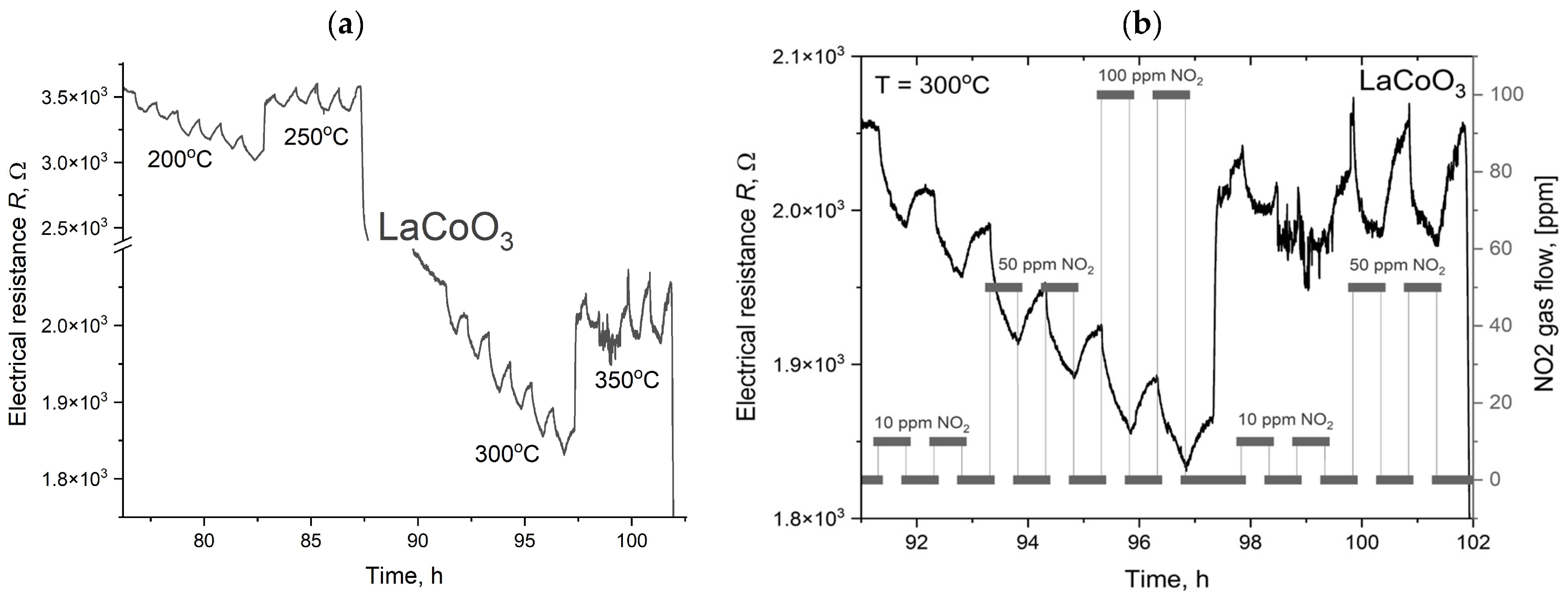
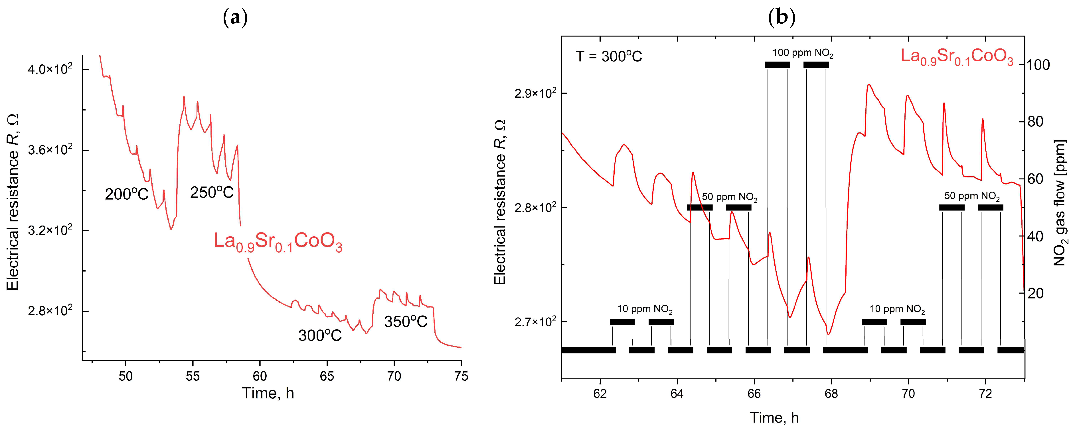
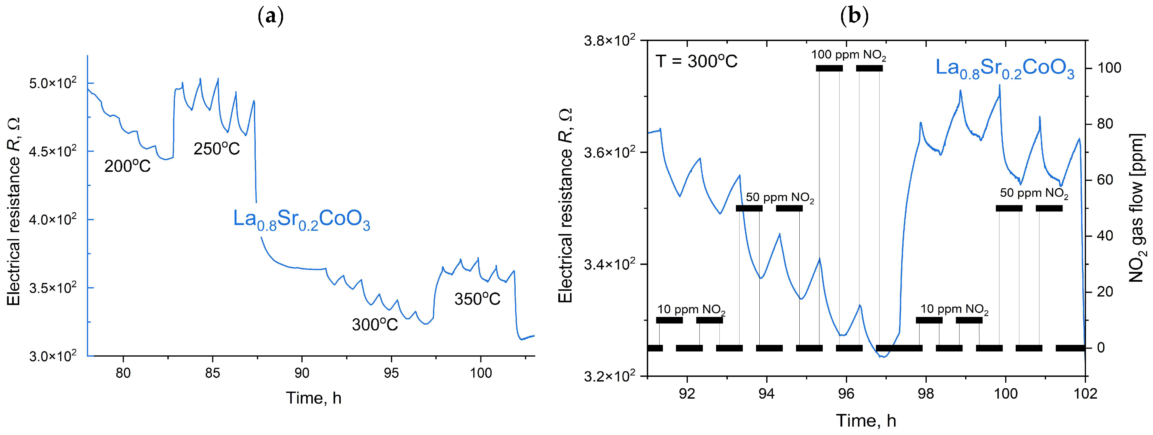
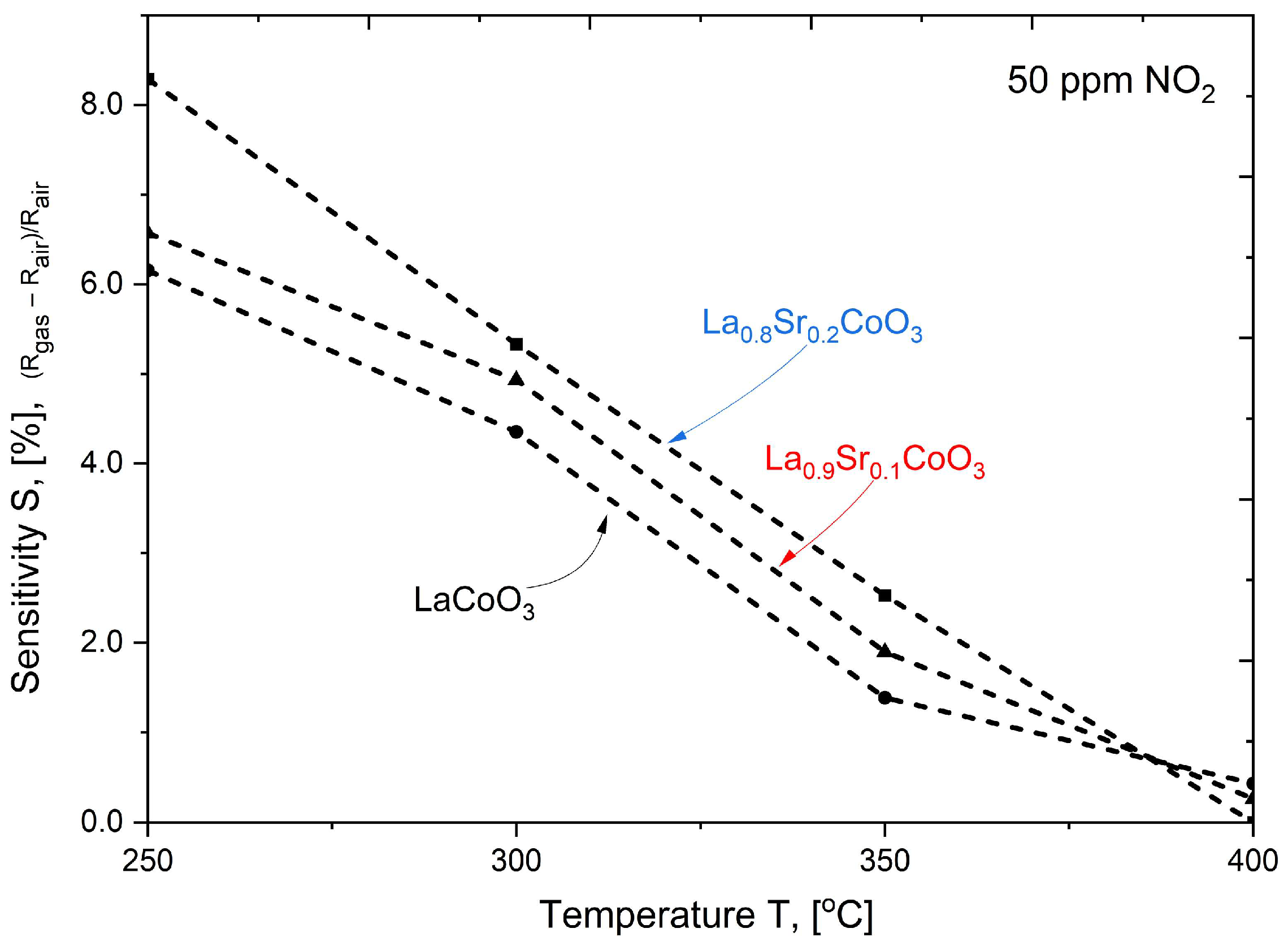
The measurement procedure was computer-controlled and executed in a predefined sequence. Initially, the test chamber was heated to the target setpoint temperature and allowed to stabilize. Subsequently, a gas dosing sequence started, in which test and reference gases were alternately introduced into the chamber. To facilitate rapid gas exchange, a constant total flow rate of 50 sccm was maintained. Throughout the process, electrometers continuously and synchronously recorded the sample’s resistance. The sensor response was defined as the ratio of the layer’s resistance in the test gas to its resistance in the reference gas (synthetic air) at an identical temperature and humidity. To ensure minimal interference in the measurements, high-purity ALPHAGAZ™ 2 gases (Air Liquide, Krakow, Poland) were used, with impurities below 1 ppm for N2, O2, and Ar, and under 0.1 ppm for hydrocarbons and moisture. The collected resistance data were then processed to determine the sensor’s response characteristics under varying gas concentrations, temperatures, and humidity levels. This method ensures highly controlled and reproducible conditions for evaluating gas-sensing materials, enabling precise characterization of their performance.
5. Summary and Discussion
La(Sr)CoO3 perovskites exhibit enhanced sensitivity to a broad range of gases, including volatile organic compounds (VOCs), nitrogen oxides, and carbon monoxide. Their unique crystal structure and surface properties facilitate strong interactions with gas molecules, inducing significant changes in electrical conductivity. In contrast, conventional metal oxides—typical sensor materials—often show limited sensitivity or require high operating temperatures, which restricts their practical application.
A key advantage of perovskites is that their selectivity toward specific gases can be finely tuned through compositional modifications, such as doping. This tunability stems from the ability to alter the oxygen binding energy and engineer oxygen vacancies within the crystal lattice, creating active sites for selective interactions. Achieving a comparable level of selectivity with traditional metal oxides is considerably more challenging due to their limited compositional and structural flexibility.
Perovskite-based sensors offer distinct advantages over traditional metal oxide sensors, particularly in terms of compositional flexibility, operating temperature, and response kinetics. The versatile perovskite crystal structure allows for a high degree of compositional flexibility by accommodating a wide range of metallic and non-metallic elements within its lattice. This adaptability enables the precise tuning of the sensor’s properties to meet the requirements of specific applications. In contrast, traditional metal oxides typically possess a more rigid stoichiometry, which inherently limits the flexibility of sensor design. Perovskite-based sensors can operate stably at significantly lower temperatures compared to their traditional oxide counterparts. This characteristic drastically reduces power consumption and extends the sensor’s operational lifespan. Conversely, traditional metal oxides often necessitate high operating temperatures to achieve optimal performance, which leads to greater energy demands and can introduce long-term stability concerns. Perovskites frequently demonstrate faster response and recovery times to fluctuations in gas concentration. This rapid kinetic response is critical for applications requiring real-time monitoring of dynamic environments. The slower kinetics of traditional oxide sensors, however, can limit their effectiveness and utility in such scenarios.
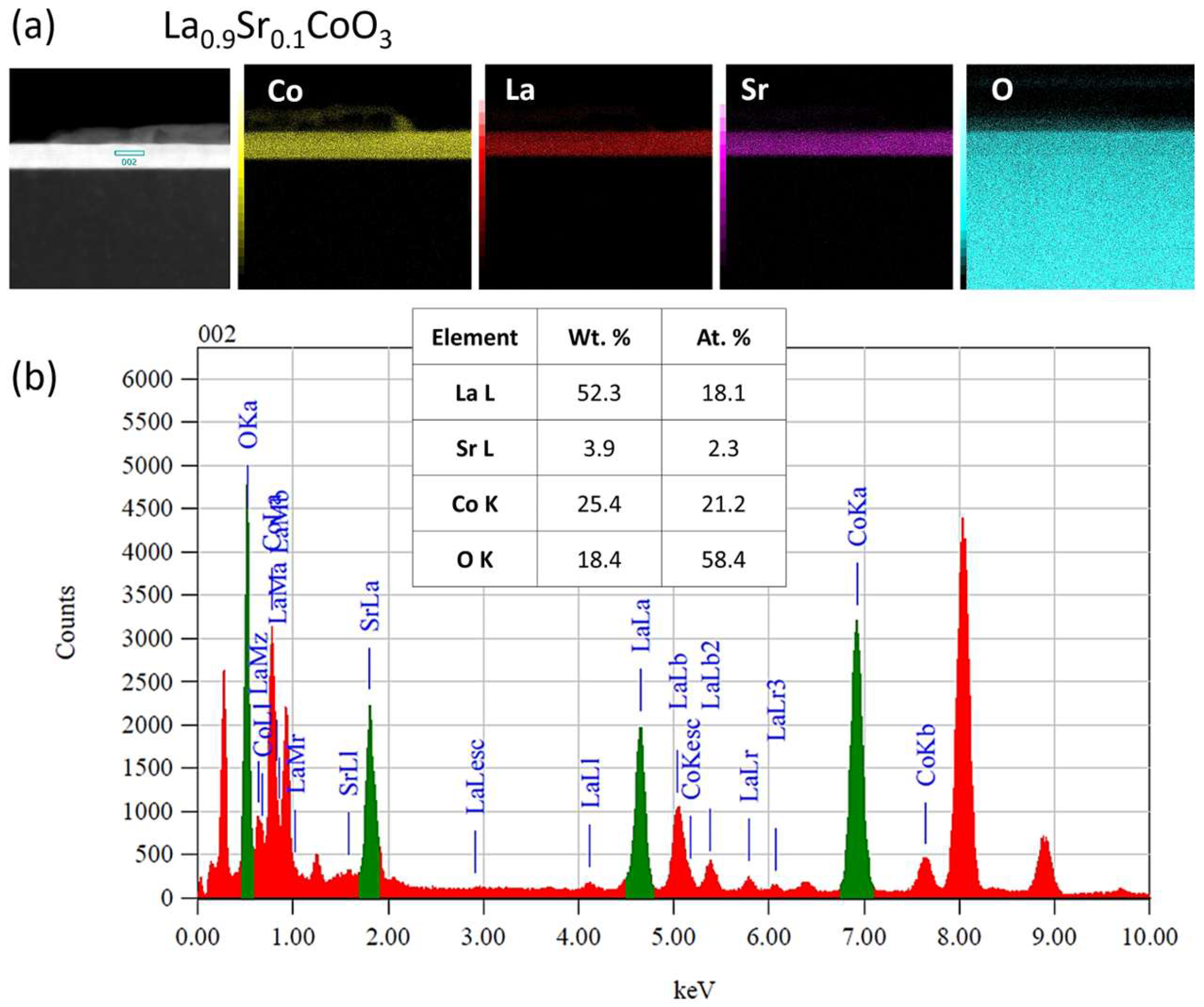
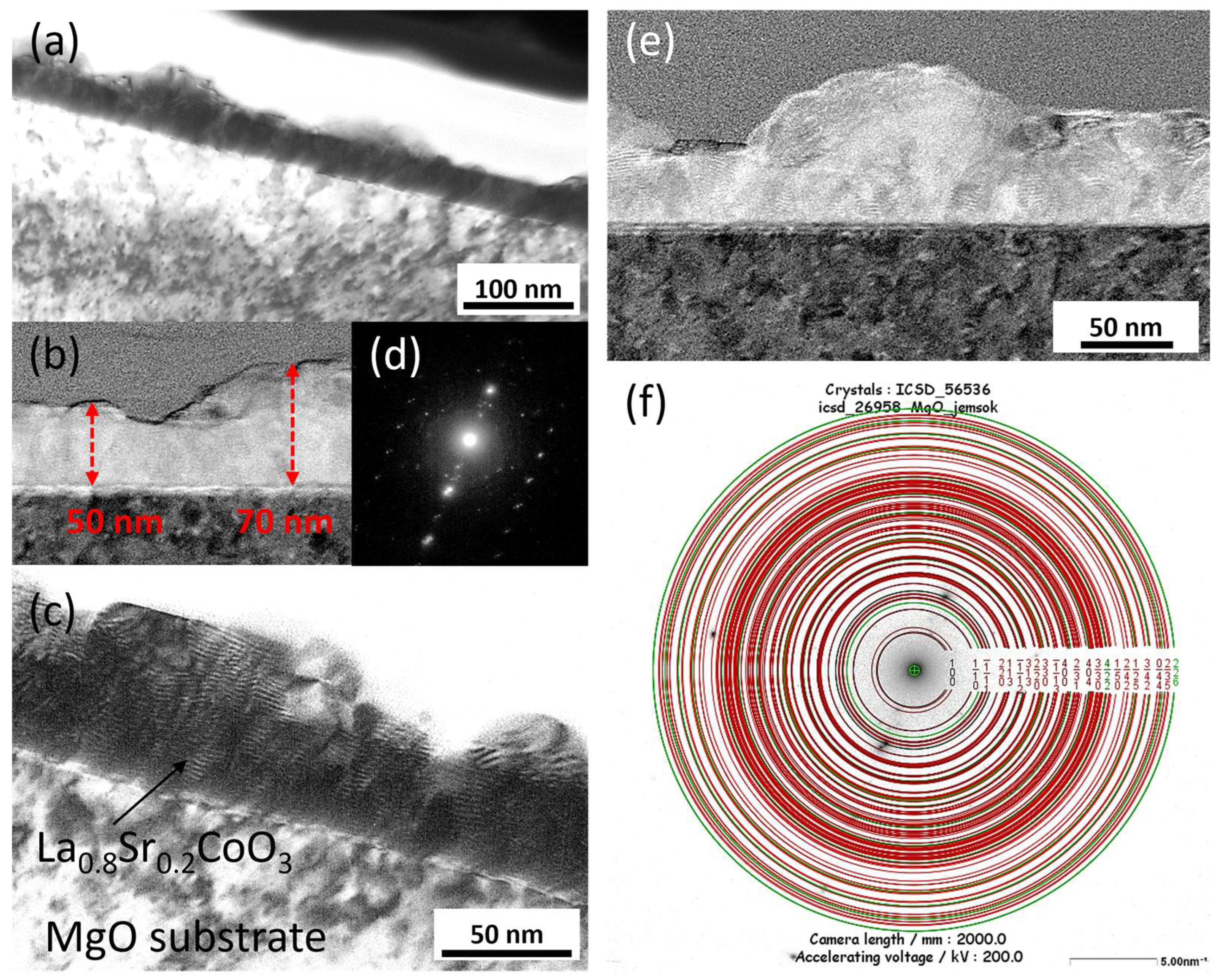
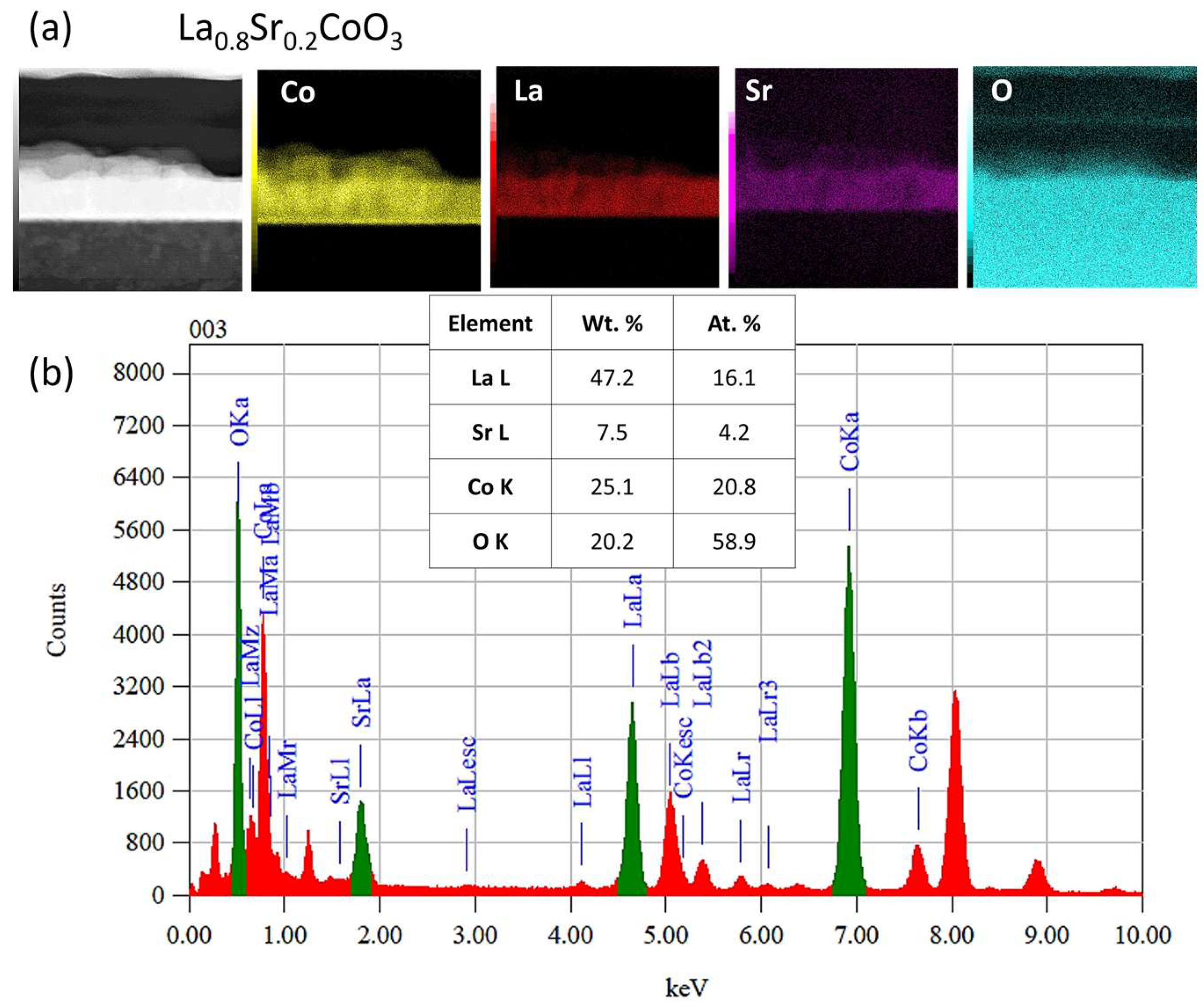
Modeling the electrical resistance of La(Sr)CoO3 perovskite thin films with varying strontium concentrations presents a complex problem. This complexity is primarily driven by changes in the material’s ionic structure, especially the formation of oxygen vacancies. Such modifications can compromise the integrity of the fundamental perovskite structure, a significant effect observed even with low Sr dopant levels of only a few atomic percent. Therefore, this study deliberately utilized Sr concentrations engineered to achieve the specific stoichiometries of La0.9Sr0.1CoO3 and La0.8Sr0.2CoO3. The successful synthesis of these compositions was confirmed through the material analyses (XRD, SEM/EDS, TEM, AFM, and XPS) presented in earlier chapters.
The concentration of the strontium (Sr) dopant is critical to the material’s properties; however, both excessively low and high levels present challenges. At low concentrations (1–5% Sr), obtaining significant and repeatable changes in resistance is difficult, as the substrate can interfere with the measurements. Conversely, excessive doping (approaching or exceeding 40–50% Sr) causes significant distortions in the cation sublattice and increases the risk of surface defects [
27]. These defects can generate unfavorable tensile stresses that counteract the benefits of increasing the number of chemically active surface sites, which is crucial for catalytic applications. As a result, structural changes dominate the measurements, leading to significant errors. Based on the stoichiometry of the obtained films, Sr dopant concentrations in the 4–10% range were selected for this study. This range demonstrated significant changes in conductivity (resistivity in the presence of NO
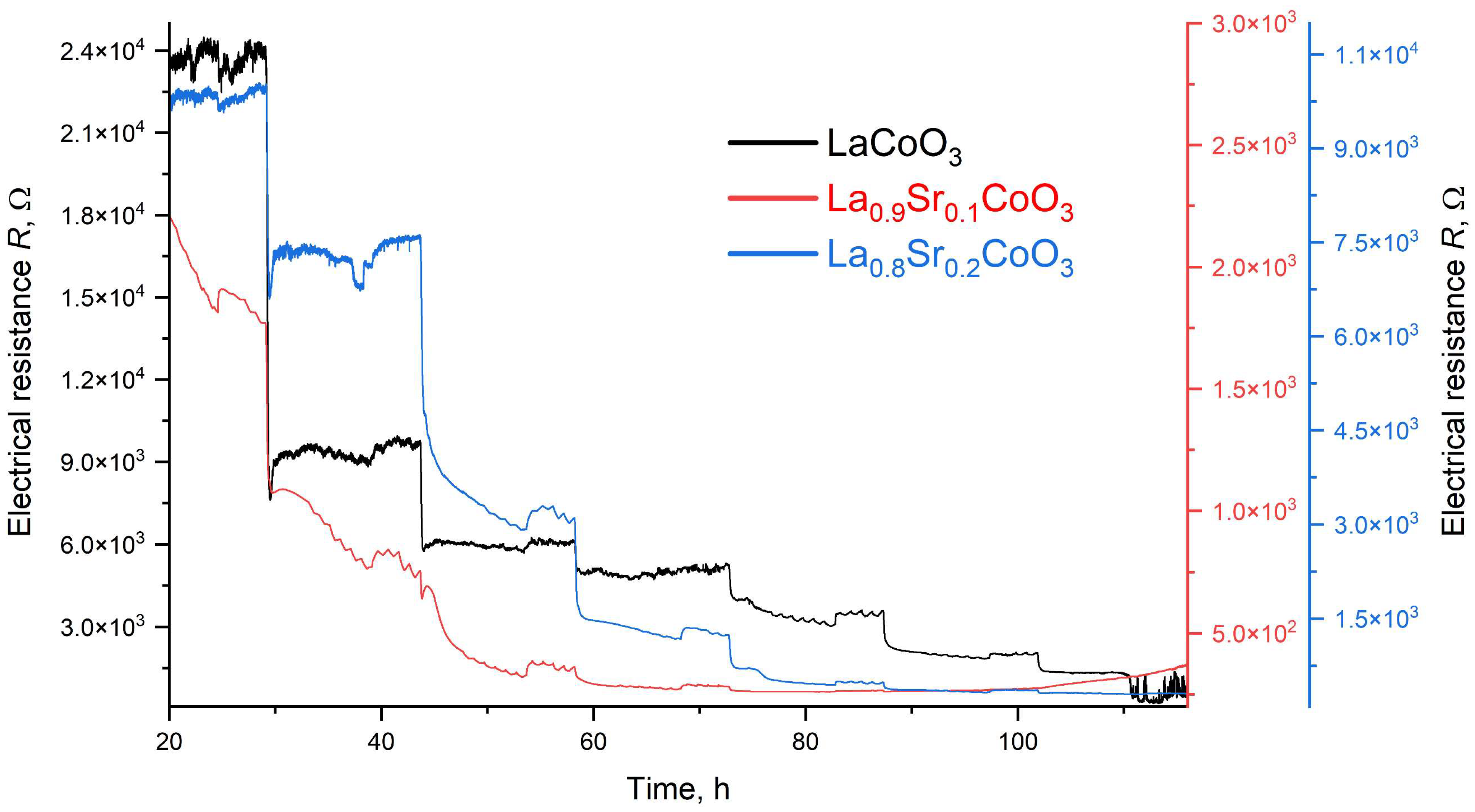
2), which will allow for a planned, systematic narrowing of this window in future research. The increased strontium concentration modifies the resistance by affecting the hopping of charge carriers between cobalt (Co) ions of different valences, as discussed in the XRD analysis. It is also worth noting that at higher temperatures (above 500 °C), polaron transport may become the dominant mechanism, particularly in materials with a high defect concentration (reaching several tens of percent). These observations suggest an optimal strontium doping range of a few percent to approximately 15%. This range provides a balance between high conductivity and the preservation of a compact structure, homogeneity, and controlled surface roughness. Exceeding or falling below this range can lead to uncontrolled growth in the material’s resistance.
The electrical properties of La(Sr)CoO3, particularly its resistance, are highly dependent on external factors, most notably temperature. This relationship, which is incorporated into our modeling, was investigated over a broad measurement range of 100–450 °C. This range corresponds to the observed, repeatable changes in the material’s catalytic properties in response to specific external stimuli. Acknowledging this is crucial for potential applications in resistive sensors. In such devices, size and weight constraints necessitate the use of lightweight, chemically resistant substrate materials (e.g., light non-ferrous metal alloys or polymer-based composites), which practically limits the operating temperature to below 500 °C.
A key challenge for the long-term application of Sr-doped LaCoO3 thin films as gas sensors is their degradation and the alteration of their catalytic properties during operation. The degradation process is complex and depends on multiple factors, including environmental conditions (e.g., temperature, atmosphere) and thermal cycling. High temperatures, often exceeding the material’s recommended operating range, accelerate degradation mechanisms such as ion diffusion, phase changes, and oxidation. The presence of moisture, CO2, SOx, and other corrosive gases can induce reactions with the perovskite, leading to adverse changes in its composition and structure. Furthermore, repeated temperature fluctuations can generate mechanical stress, causing cracking and delamination of the film. Consequently, this study does not focus on the predictive modeling of structural changes but rather on verifying the actual layer growth conditions to obtain ideal structures. The goal is to produce films with properties that correlate with the predicted changes in catalytic activity in the presence of NO2 within a specific temperature range. A thorough understanding of these factors is essential for optimizing the electrical properties of La(Sr)CoO3 thin films for their use in electronic and electrochemical devices.
To enhance the response and reaction times of thin-film La(Sr)CoO3 perovskite sensors, optimizing their topography and minimizing ionic structural defects are critical. Both characteristics directly influence analyte diffusion rates, charge transport, and overall sensor performance. The topography of the sensing film—including its porosity, grain size, and total surface area—plays a fundamental role in determining sensor reaction time. A more porous or nanostructured surface, such as those with nanotube or nanorod architectures, offers a higher surface-area-to-volume ratio. This facilitates faster and more efficient adsorption of analyte molecules, directly shortening the response time. However, a high density of grain boundaries in polycrystalline films can act as trapping centers for charge carriers, thereby slowing the sensor’s reaction. This appears to be the primary cause of the extended response and reaction times observed in our research (~30 min), despite the films’ stability. Fabricating films with slightly larger, well-interconnected nanocrystallites can streamline charge transport and accelerate response times. Film thickness is also a key parameter. An excessively thick film can impede the diffusion of the analyte to active sites, whereas a film that is too thin may not offer enough interaction sites due to its limited topographical development.
Defects within the perovskite crystal lattice, such as ion vacancies, critically affect the sensor’s electronic properties and reaction time. These imperfections promote the formation of localized energy states within the band gap, which can trap electrons and holes. This trapping mechanism slows their transport to the electrodes and lengthens the time required to generate a measurable signal. Furthermore, these defects often serve as non-radiative recombination centers, reducing the number of charge carriers that contribute to the sensory signal. This can decelerate both the response and recovery times. Additionally, the mobility of ionic defects under an electric field can lead to signal instability and hysteresis, complicating accurate and rapid measurements. Based on these findings, we propose two primary modification strategies for the La(Sr)CoO3 thin films analyzed in this study. Compositional engineering—refining the doping range to precisely tune the material’s stoichiometry. This should be based on the two most promising doping variants identified in our work (La0.9Sr0.1CoO3 and La0.8Sr0.2CoO3), focusing on films that have already demonstrated superior structural characteristics. Precise control over the substrate’s annealing temperature and duration, both during the pre-deposition cleaning and the post-deposition stages, is crucial. This will allow for targeted management of grain growth and the final microstructure of the film.
The degradation of thin-film perovskite films in gas sensors exposed to nitrogen dioxide (NO2) is a complex chemical and structural process. The primary cause is the highly oxidizing nature of the NO2 molecule, which reacts with the perovskite surface, leading to irreversible damage and a loss of sensing capabilities. The degradation mechanism is a multi-stage process driven by several key phenomena. As strong electron acceptors (oxidants), NO2 molecules first adsorb onto the perovskite surface and withdraw electrons from its crystal lattice. This removal of electrons destabilizes the delicate ionic balance within the perovskite structure, often leading to the material’s decomposition. This process forms new surface phases that are inactive for sensing, causing permanent changes to the layer’s morphology and electronic properties. Consequently, the sensor exhibits reduced sensitivity, slower response and recovery times, and poor long-term stability. The degradation process is significantly accelerated by the presence of moisture. Water (H2O) can facilitate chemical reactions on the perovskite surface and promote the formation of hydrated intermediate forms. These hydrated perovskites are typically unstable and decompose readily, hastening the overall decay of the sensor material.
Several strategies are employed to increase the stability of perovskite gas sensors and their resistance to NO2. One primary approach is chemical composition engineering. Modifying the material’s formula—for example, by replacing an unstable cation or creating mixed, non-stoichiometric compositions—can significantly improve the thermal and chemical stability of the perovskite structure. Another effective method is the synthesis of two-dimensional (2D) or mixed quasi-2D/3D structures. In these architectures, long organic molecules act as natural barriers, shielding the perovskite material from moisture and aggressive gases and thereby extending its operational lifetime. In this context, the applied electron ablation method appears to be highly encouraging, as shown by the present structural studies. Finally, morphology control is crucial. The creation of dense, uniform perovskite layers with large, well-defined crystallites minimizes the number of grain boundaries. Since grain boundaries are preferential sites for initiating degradation, a high-quality film morphology enhances the material’s overall robustness. By combining these strategies, it is possible to significantly extend the service life and improve the reliability of thin-film perovskite NO2 sensors, moving them closer to practical commercial applications.
Strontium-doped LaCoO3 perovskite thin films show significant potential for various applications, particularly in gas sensing (for NOx, CO, and VOCs), environmental monitoring, and as temperature and humidity sensors. Sr doping enhances the material’s conductivity and reactivity, leading to improved sensitivity and selectivity. The key mechanism involves the introduction of Sr dopant into the LaCoO3 structure, which allows for the control of oxygen ion mobility by generating oxygen vacancies responsible for the material’s chemical activity. Despite these advantages, thin films are particularly susceptible to degradation due to their large surface area in contact with the environment. Typical degradation processes include ion diffusion, reactions with ambient gases (e.g., moisture and CO2, leading to the formation of carbonates or hydroxides), chemical poisoning of active sites, and high-temperature grain sintering, which reduces the active surface area. These phenomena manifest as a significant decrease in catalytic activity, a deterioration in selectivity and stability, and a shortened film lifespan. To counteract degradation, it is crucial to fabricate films with a high-quality internal structure—specifically, a dense, columnar, and defect-free crystal morphology. Such conditions can be achieved through controlled epitaxial growth using Pulsed Electron Deposition. The material analyses presented in this work confirm the effectiveness of an optimized PED process for producing high-quality La(Sr)CoO3 thin films. This achievement is particularly noteworthy because electron beam ablation is often considered more challenging to control and less reproducible than the more common pulsed laser deposition technique. Therefore, optimizing the perovskite’s chemical composition and structure through a well-defined fabrication process is essential for limiting degradation and ensuring long-term stability.
Thin films of LaCoO3 perovskite are fabricated using various methods, including magnetron sputtering, atomic layer deposition (ALD), molecular beam epitaxy (MBE), and physical vapor deposition (PVD) based ablative techniques such as pulsed laser deposition (PLD) and pulsed electron deposition (PED). Ablative techniques are particularly advantageous as they minimize gas-phase decomposition, ensuring a precise stoichiometric transfer from the target to the substrate when optimized. Furthermore, these methods offer exceptional control over film thickness by adjusting parameters like power density, working distance, and the number of pulses. This precision is critical for the seamless integration of La(Sr)CoO3 films with microelectromechanical systems (MEMS), facilitating miniaturization and integration with other electronic components. From a manufacturing perspective, ablative techniques are scalable and relatively cost-effective. This financial advantage is amplified by the low cost of perovskite materials, making the approach well-suited for the mass production of thin films. Moreover, recent developments in fabricating these films on flexible substrates are paving the way for novel applications, such as wearable sensors integrated into everyday textiles.
