Abstract
Electrochromic capacitors, which are capable of altering their appearances in line with their charged states, are drawing substantial attention from both academia and industry. Tungsten oxide is usually used as an electrochromic layer material for electrochromic devices, or as an active material for high-performance capacitor electrodes. Despite this, acceptable visual aesthetics in electrochromic capacitors have almost never been achieved using tungsten oxide, because, in its pure form, this compound only displays a onefold color modulation from transparent to blue. Herein, we have designed W/WO3/TiO2 multilayer films by a magnetron sputtering device. The impact of TiO2 layer on the optical and electrochemical properties was investigated. The results show that the optimum thickness of the TiO2 layer is 10 nm. The as-prepared film displays a high coloration efficiency (CE) of 74.2 cm2 C−1, a high areal capacitance of 32.0 mF/cm2, an excellent rate performance (with the areal capacitance still retaining 87% of the maximum capacitance at a current density of 1 mA/cm2), and a high cycle life (with a capacity retention of 91% after 1000 cycles).
1. Introduction
Electrochemical capacitors are among the key energy storage technologies that significantly contribute to addressing the pressing need for high-power-density solutions [1,2]. Supercapacitors can be divided into double electric-layer capacitors (DELCs) and pseudocapacitors [3,4]. Wang et al. reported activated carbon fibers (ACFs) with high micropore specific surface area and micropore volume that showed a high specific capacitance of 249 F g−1 at a current density of 0.05 A g−1 [5]. Thillaikkarasi, D. et al. fabricated an electrical double-layer capacitor with biomass-derived activated carbon (AC) and multi-walled carbon nanotubes (MWCNTs) that showed outstanding performance [6]. Pseudocapacitors achieve energy storage through reversible redox reactions [7,8]. Compared with double electric-layer capacitors that rely solely on the adsorption/desorption of ions to store energy, pseudocapacitors have higher specific capacity and broader application prospects. Pham, H.D. et al. designed a potassium-ion capacitor (KIC) using layered potassium niobate (K4Nb6O17, KNO) nanosheet arrays as anode and orange peel-derived activated carbons (OPACs) as fast capacitive cathode materials delivering both a high energy density of 116 Wh/kg and a high power density of 10,808 W/kg [9]. Some pseudocapacitive electrode materials can undergo reversible changes in ionic valence during charging and discharging processes, which can be accompanied by the generation of electrochromic (EC) phenomena [10,11]. Similar to the working principle of pseudocapacitive electrode materials, this type of electrochromic phenomenon is closely related to the intercalation and deintercalation of ions/electrons in active materials under external electric fields [12].
Supercapacitors with electrochromic properties can display the energy storage state of the supercapacitor through color changes [12,13,14,15,16]. For both supercapacitors and electrochromic devices, electrode materials, as the core of the device, directly affect the performance of the device. Transition metal compounds, characterized by high theoretical specific capacitance, rich valence states, easily obtainable raw materials, and low preparation costs, are often used as electrode materials for electrochromic supercapacitors. WO3 is frequently utilized in electrochromic supercapacitors, as it functions effectively as an active material for both establishing benchmarks in electrochromic device performance and enhancing the efficiency of supercapacitor electrodes [17]. However, the low conductivity and easy agglomeration of transition metal compounds generally limit their electrochemical performance.
The short service life limits the application of WO3 films. The electrochemical activity of WO3 film decreases with the process of charging and discharging [18]. The high stability and biocompatibility of TiO2 have attracted the attention of researchers. It has been reported that the service life of WO3 films can be improved by doping TiO2 [18,19,20,21]. However, the concentration of Ti doping seriously affects the properties of WO3 films [22].
Herein, W/WO3/TiO2 electrochromic supercapacitor complex films were fabricated by PVD, and the properties of these films were examined. The metal layer causes a distinct interference resonance, thus displaying a distinct structural color. The surface TiO2 layer can effectively prevent the WO3 layer from corrosion by acidic electrolytes. The interface effect of the hierarchical structure of W/WO3/TiO2 film provides a convenient method for the diffusion and charge transfer of ions. Complex films of W/WO3/TiO2 are capable of altering their structure in response to charge/discharge cycles, while also exhibiting superior electrochemical and electrochromic properties. These properties include elevated coloration efficiency, extended cycle life, and enhanced areal capacitance, all of which are achieved with the optimal thickness of the TiO2 layer.
2. Materials and Methods
ITO glass substrates (South China Science & Technology Co., Ltd., Shenzhen, China) were cut to a size of 2.0 × 1.0 cm2 and were used as electrodes. Before use, the ITO glass substrates were ultrasonically cleaned in acetone solution for 15 mins, in anhydrous alcohol for 15 min, and then in deionized water for 15 min. Finally, the substrates were dried in a nitrogen atmosphere. The W/WO3/TiO2 (10 nm) multilayer film electrodes were fabricated by a magnetron sputtering device. The details of the synthetic procedure were as follows: Metallic tungsten (W) films were deposited on clean ITO glass substrates by sputtering the W target (99.9%, ZhongNuo Advanced Material (Beijing) Technology Co., Ltd., Beijing, China) at 100 W and under 0.2 Pa. All WO3 films were prepared on W film by sputtering the W target (99.9%) at 100 W under 0.3 Pa. Then, TiO2 films were prepared on WO3 film by sputtering the TiO2 target (99.99%, ZhongNuo Advanced Material (Beijing) Technology Co., Ltd., Beijing, China) at 100 W under 0.3 Pa. By adjusting the deposition duration, the TiO2 layer was manipulated to range between 0 nm and 40 nm. The thickness of the TiO2 film was set at 0 nm, 6 nm, 10 nm, 20 nm, 30 nm, and 40 nm, corresponding to samples labeled as Film 1, Film 2, Film 3, Film 4, Film 5, and Film 6, respectively. The thickness and growth rate of the films were monitored using a quartz crystal oscillator film-thickness apparatus (FTM-V, Taiyao Vacuum Tech, Shanghai, China).
A field emission scanning electron microscope (FESEM, ZEISS MERLIN Compact, Jena, Germany) was used to observe the morphology of the films. The crystal and phase formations were recorded by X-ray diffraction (XRD, Bruker D8 ADVANC, Karlsruhe, Germany) with Cu Ka radiation (λ = 0.15405 nm), and the scanning speed was 2°/min. The optical properties of the films were recorded by a fiber optical spectrometer (AvaSpec-Mini2048CL-V125, Avantes, Beijing, China). The three-electrode system of an electrochemical workstation (CS310; Wuhan Corrtest Instruments Corp, Ltd., Wuhan, China) was employed in a 1 M H2SO4 solution for the electrochromic and electrochemical performance measurements of the hierarchical structure films. During these measurements, platinum (Pt) and silver/silver chloride (Ag/AgCl) were utilized as the counterelectrode and reference electrode, respectively. All optical images of complex film were obtained by camera.
3. Results and Discussion
As can be seen from Figure 1, all films have a smaller nanoparticle size and exhibit uniform, compact, and smooth features. However, there are some differences in the morphology of different samples. As can be seen from Figure 1, the surface of the ITO/W/WO3/TiO2 complex films are rougher than that of the ITO/W/WO3 film, and the surface of the sample becomes rougher as the thickness of the TiO2 increases. The phase composition of individual ITO substrates, ITO/W, ITO/W/WO3, and ITO/W/WO3/TiO2 complex film, was characterized using X-ray diffraction (XRD), as shown in Figure 2. The XRD patterns of all films are highly consistent with the ITO (JCPDS#01-008-2160 and JCPDS#00-039-1058). The XRD patterns reveals no distinct characteristic peaks of the WO3 or TiO2 layers, indicating the amorphous structure of the WO3 and TiO2 layers.
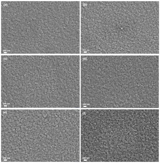
Figure 1.
SEM micrographs of different samples: (a) Film 1, (b) Film 2, (c) Film 3, (d) Film 4, (e) Film 5, (f) Film 6.
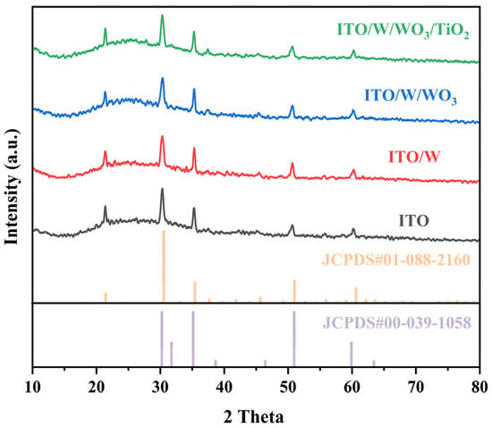
Figure 2.
XRD patterns of ITO, ITO/W film, ITO/W/WO3 film, and ITO/W/WO3/TiO2 hierarchical structure film.
The cross-section SEM image of the electrode in Figure 3 shows a perfect three-layer structure consisting of a thin W layer, a thin WO3 layer, and a thin TiO2 layer, with small thickness variation. The corresponding EDX mapping also indicates that a uniform distribution is achieved for the thin W layer, the thin WO3 layer, and the thin TiO2 layer in the ITO/W/WO3/TiO2 film. The thickness of the film, measured by a quartz crystal oscillator film-thickness apparatus, is consistent with that measured by the cross-section SEM image.
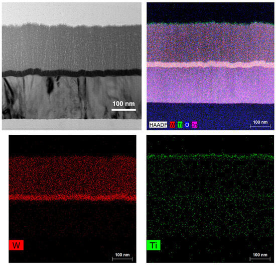
Figure 3.
Structural characterizations of ITO/W/WO3/TiO2: cross-sectional SEM and corresponding elemental mapping images of W, O, and Ti.
Figure 4 shows the reflection spectra of Film 1, Film 2, Film 3, Film 4, Film 5, and Film 6. For the electrode with a 0 nm TiO2 thickness, there are multiple reflectance peaks and valleys in the reflection spectrum across the wavelength range of 350–800 nm, which are caused by the tungsten metal layer. Upon increasing the thickness of the TiO2 layer, the location of the reflection peaks and valleys are redshifted. The color changes from violet to blue by increasing the thickness of the TiO2.
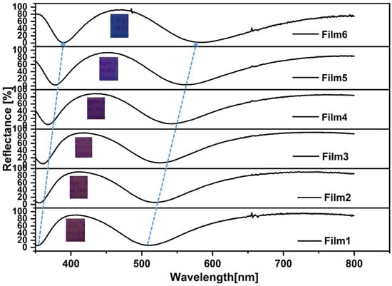
Figure 4.
Reflection spectra (inset: optical images) of different samples: Film 1, Film 2, Film 3, Film 4, Film 5, Film 6.
Figure 5 shows the reflection spectra of six thin film electrodes at different potentials. As the voltage gradually decreases to 0, −0.1, −0.2, −0.3, −0.4, and −0.5 V, the reflectance spectrum of the electrode gradually redshifts and the primary reflectance key decreases. Figure 6 shows optical images of six thin film electrodes at different potentials. It can be seen that during the discharge process, the electrode can produce a multicolor state. Accordingly, its reflection spectrum displays a drastic hypsochromic shift in the peak position, achieving very large modulation range (200 nm) compared with the values previously reported for inorganic electrochromic materials. Its color changes are directly related to the large change in the refractive index of the WO3 layer [23]. The refractive index of the WO3 layer is found to vary with the amount of hydrogen inserted.
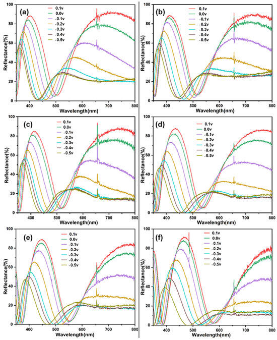
Figure 5.
Reflection spectra of different samples with different potentials: (a) Film 1, (b) Film 2, (c) Film 3, (d) Film 4, (e) Film 5, (f) Film 6.
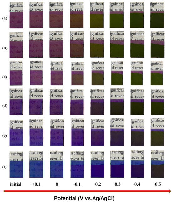
Figure 6.
Optical images of different samples with different potentials: (a) Film 1, (b) Film 2, (c) Film 3, (d) Film 4, (e) Film 5, (f) Film 6.
Characteristic cyclic voltammogram (CV) curves of multilayer films between −0.4 V and +0.4 V at different scanning rates (10, 20, 30, 50, 80, and 100 mVs−1) are shown in Figure 7. All electrode films show broad and featureless CV curves. The CV curves of the films are similar to stoichiometric and nonstoichiometric tungsten oxide analogues [24,25]. All electrode films exhibit distinct oxidation peaks, with no apparent reduction peak. As the potential decreases from +0.4 V to −0.4 V, a significant increase takes place in the cathodic current density associated with the H+ ions, and electrons intercalate into the films. Reversing the potential from −0.4 V to +0.4 V, the H+ ions and electrons deintercalate out of the films due to the oxidation. These processes lead to the films’ color change. The oxidation peak shifts continuously to higher potentials with the increasing scanning rate. With the increase in the scanning rate, the peak current density gradually increases, indicating that the number of protons and electrons embedded in the film increases, and further indicates that the reactivity of the film is enhanced. The plot of the peak current Ip as a function of the square root of the scan rate v1/2 is provided in the insets in Figure 7. Ip is in direct proportion to v1/2, confirming the diffusion-controlled behavior.
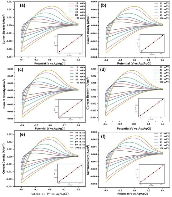
Figure 7.
CVs with different scan rates (peak current Ip as function of square root of scan v1/2 tested in the inset) for different samples: (a) Film 1, (b) Film 2, (c) Film 3, (d) Film 4, (e) Film 5, (f) Film 6.
The optical density (ΔOD) of Film 1 and Film 3 in relation to the charge density at a monitoring wavelength of 750 nm is depicted in Figure 8. Film 1 exhibits a color-rendering efficiency of 44.1 cm2 C−1, which is consistent with previous reports (CNT/WO3 17.3 cm2 C−1, WO3/W 48.6 cm2 C−1) and the normal current collector-covered electrochromic electrodes (FTO/WO3 36.1 cm2 C−1, ITO/WO3 47.1 cm2 C−1) [23,26]. Film 3 demonstrates a higher efficiency of 74.2 cm2 C−1. Notably, the W/WO3/TiO2 electrode displays superior color-rendering efficiency compared to the W/WO3 electrode, suggesting that an appropriate thickness of the TiO2 layer can effectively enhance its coloring performance.
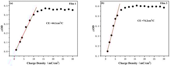
Figure 8.
Optical density variation (∆OD) vs. charge density of (a) Film 1 and (b) Film 3 when monitored at a wavelength of 750 nm.
Areal capacitances obtained by the galvanostatic charge/discharge (GCD) curves were used to evaluate the capacitance performances of the complex films, as shown in Figure 9. The areal capacitance of the complex films (0.2 mA/cm2) were calculated to be 30.4 mF/cm2, 31.9 mF/cm2, 32.0 mF/cm2, 34.1 mF/cm2, 35.9 mF/cm2, and 38.1 mF/cm2. These values indicate that the films’ properties align with those of other tungsten oxide-based supercapacitor electrodes. The areal capacitances of complex films with different current densities were calculated and are shown in Figure 10. Areal capacitance decreases gradually with the increase in discharge current density. The areal capacitance of the W/WO3 film retains 68% of the maximum capacitance at a current density of 1 mA/cm2, while the areal capacitance of the W/WO3/TiO2 (10 nm) film retains 87%. This result shows the perfect rate performance of a film electrode with the optimal thickness of the TiO2 layer.
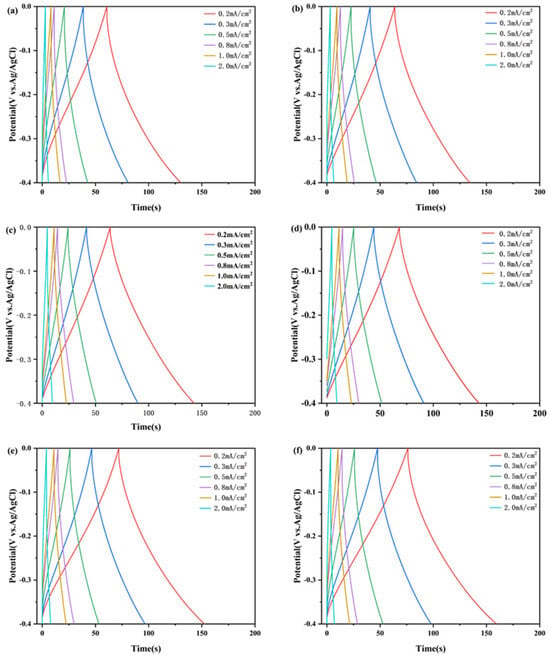
Figure 9.
GCD curves of different samples: (a) Film 1, (b) Film 2, (c) Film 3, (d) Film 4, (e) Film 5, (f) Film 6.
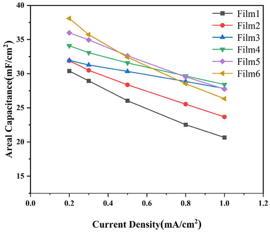
Figure 10.
Areal capacitance of samples with different current densities.
Continuous cyclic voltammograms (CVs) with a scan rate of 100 mVs−1 were used to characterize the stability of Film 1 and Film 3, as shown in Figure 11. Following 1000 cycles, the capacity of Film 1 decreased to 81%, whereas the good stability of Film 3 is demonstrated by a high capacity retention of 91% after 1000 cycles. The surface layer of titanium dioxide can effectively avoid direct contact with electrolytes and protect the WO3 film.
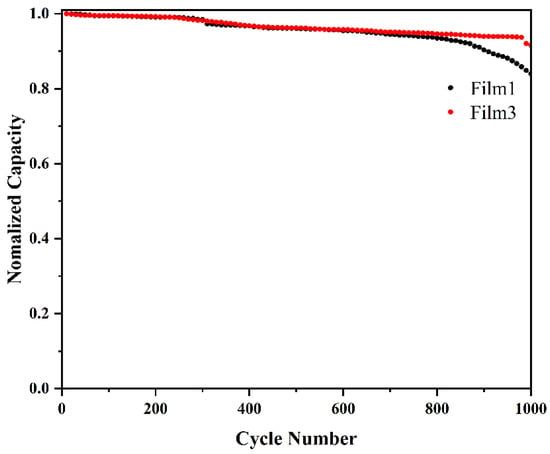
Figure 11.
Normalized charge capacity of Film 1 and Film 3 over 1000 cyclic voltammograms (CVs) at a scan rate of 100 mv s−1 with the potential range of −0.4 V~+0.4 V.
4. Conclusions
In conclusion, W/WO3/TiO2 complex films were fabricated. The optical and electrochemical properties of WO3 thin films are greatly influenced by the appropriate thickness of surface TiO2. The results show that the optimum thickness of the TiO2 layer is 10 nm. The as-prepared film displays a high coloration efficiency (CE) of 74.2 cm2 C−1, a high areal capacitance of 32.0 mF/cm2, an excellent rate performance (with the areal capacitance retaining 87% of the maximum capacitance at a current density of 1 mA/cm2), and a high cycle life (with a capacity retention 91% after 1000 cycles).
Author Contributions
Z.W.: methodology, formal analysis, writing—original draft preparation, and writing—review and editing; G.L.: methodology and formal analysis; C.L.: software and data curation; M.Q.: data curation and validation; M.T.: data curation and validation; X.L.: investigation; W.C.: data curation and validation; X.W.: software and data curation; J.L.: software and data curation; S.X.: methodology and formal analysis. All authors have read and agreed to the published version of the manuscript.
Funding
This work was supported by the National Natural Science Foundation of China (grant numbers 12274085, 52202163, and 12104085), the “Belt and Road” innovative talent exchange program for foreign experts (grant number DL2023023007L) the Natural Science Foundation of Shandong Province (grant numbers ZR2021QF146, ZR2021QA063, ZR2022QE125, and ZR2021QA008), and the Project of Talent Incubation of Dezhou University (grant numbers 2020xjrc201 and 2019xjrc321).
Institutional Review Board Statement
Not applicable.
Informed Consent Statement
Not applicable.
Data Availability Statement
The original contributions presented in this study are included in the article. Further inquiries can be directed to the corresponding authors.
Conflicts of Interest
The authors declare no conflicts of interest.
References
- Wang, L.J.; El-Kady, M.F.; Dubin, S.; Hwang, J.Y.; Shao, Y.; Marsh, K.; McVerry, B.; Kowal, M.D.; Mousavi, M.F.; Kaner, R.B. Flash converted graphene for ultra-high power supercapacitors. Adv. Energy Mater. 2015, 5, 1500786. [Google Scholar] [CrossRef]
- Liu, Z.; Liu, S.; Dong, R.; Yang, S.; Lu, H.; Narita, A.; Feng, X.; Müllen, K. High power in-plane micro-supercapacitors based on mesoporous polyaniline patterned graphene. Small 2017, 13, 1603388. [Google Scholar] [CrossRef] [PubMed]
- Wei, D.; Scherer, M.R.J.; Bower, C.; Andrew, P.; Ryhänen, T.; Steiner, U. A nanostructured electrochromic supercapacitor. Nano Lett. 2012, 12, 1857–1862. [Google Scholar] [CrossRef] [PubMed]
- Cheng, G.; Xu, J.; Dong, C.; Yang, W.; Kou, T.; Zhang, Z. Anodization driven synthesis of nickel oxalate nanostructures with excellent performance for asymmetric supercapacitors. J. Mater. Chem. A 2014, 2, 17307–17313. [Google Scholar] [CrossRef]
- Wang, C.; Bai, L.; Zhao, F.; Bai, L. Activated carbon fibers derived from natural cattail fibers for supercapacitors. Carbon Lett. 2022, 32, 907–915. [Google Scholar] [CrossRef]
- Thillaikkarasi, D.; Karthikeyan, S.; Ramesh, R.; Sengodan, P.; Kavitha, D.; Muthubalasubramanian, M. Electrochemical performance of various activated carbon-multi-walled carbon nanotubes symmetric supercapacitor electrodes in aqueous electrolytes. Carbon Lett. 2022, 32, 1481–1505. [Google Scholar] [CrossRef]
- Liu, K.; Yu, C.; Guo, W.; Ni, L.; Yu, J.; Xie, Y.; Wang, Z.; Ren, Y.; Qiu, J. Recent research advances of self-discharge in supercapacitors: Mechanisms and suppressing strategies. J. Energy Chem. 2021, 58, 94–109. [Google Scholar] [CrossRef]
- Bello, I.T.; Oladipo, A.O.; Adeokn, O.; Dhlamini, S.M. Recent advances on the preparation and electrochemical analysis of MoS2-basedmaterials for supercapacitor applications: A mini-review. Mater. Today Commun. 2020, 25, 101664. [Google Scholar] [CrossRef]
- Pham, H.D.; Chodankar, N.R.; Jadhav, S.D.; Jayaramulu, K.; Nanjundan, A.K.; Dubal, D.P. Large interspaced layered potassium niobate nanosheet arrays as an ultrastable anode for potassium ion capacitor. Energy Storage Mater. 2021, 34, 475–482. [Google Scholar] [CrossRef]
- Wang, J.; Zhang, L.; Yu, L.; Jiao, Z.; Xie, H.; Lou, X.W.; Sun, X.W. A bi-functional device for self-powered electrochromic window and self-rechargeable transparent battery applications. Nat. Commun. 2014, 5, 4921. [Google Scholar] [CrossRef]
- Bayrak, P.İ.; Atak, G.; Niklasson, G.A.; Stolt, L.; Edoff, M.; Edvinsson, T. Electrochromic solar water splitting using a cathodic WO3 electrocatalyst. Nano Energy 2021, 81, 105620. [Google Scholar] [CrossRef]
- Bi, Z.; Li, X.; He, X.; Chen, Y.; Xu, X.; Gao, X. Integrated electrochromism and energy storage applications based on tungsten trioxide monohydrate nanosheets by novel one-step low temperature synthesis. Sol. Energy Mater. Sol. Cells 2018, 183, 59–65. [Google Scholar] [CrossRef]
- Yang, P.; Sun, P.; Mai, W. Electrochromic energy storage devices. Mater. Today 2016, 19, 394–402. [Google Scholar] [CrossRef]
- Zhou, S.; Wang, S.; Zhou, S.; Xu, H.; Zhao, J.; Wang, J.; Li, Y. Electrochromic-Supercapacitor Based on MOF Derived Hierarchical-Porous NiO Film. Nanoscale 2020, 12, 8934–8941. [Google Scholar] [CrossRef] [PubMed]
- Wei, H.; Zhu, J.; Wu, S.; Wei, S.; Guo, Z. Electrochromic polyaniline/graphite oxide nanocomposites with endured electrochemical energy storage. Polymer 2013, 54, 1820–1831. [Google Scholar] [CrossRef]
- Zhong, Y.; Chai, Z.; Liang, Z.; Sun, P.; Xie, W.; Zhao, C.; Mai, W. Electrochromic Asymmetric Supercapacitor Windows Enable Direct Determination of Energy Status by the Naked Eye. ACS Appl. Mater. Interfaces 2017, 9, 34085–34092. [Google Scholar] [CrossRef] [PubMed]
- Chen, J.; Wang, Z.; Chen, Z.; Cong, S.; Zhao, Z. Fabry-Perot Cavity-Type Electrochromic Supercapacitors with Exceptionally Versatile Color Tunability. Nano Lett. 2020, 20, 1915–1922. [Google Scholar] [CrossRef]
- Park, S.; Thuy, D.T.; Sarwar, S.; Van Tran, H.; Lee, S.I.; Park, H.S.; Song, S.H.; Han, C.-H.; Hong, S. Synergistic effects of Ti-doping induced porous networks on electrochromic performance of WO3 films. J. Mater. Chem. C 2020, 8, 17245–17253. [Google Scholar] [CrossRef]
- Han, J.; Ko, K.-W.; Sarwar, S.; Lee, M.-S.; Park, S.; Hong, S.; Han, C.-H. Enhanced electrochromic properties of TiO2 nanocrystal embedded amorphous WO3 films. Electrochim. Acta 2018, 278, 396–404. [Google Scholar] [CrossRef]
- Sun, X.; Wang, D.; Wu, W.; Zhao, X.; Zhang, X.; Wang, B.; Rong, X.; Wu, G.; Wang, X. Amorphous and Crystalline Ti-Doped WO3·2H2O for Dual-Band Electrochromic Smart Windows. ACS Sustain. Chem. Eng. 2024, 12, 5459–5467. [Google Scholar] [CrossRef]
- Liu, L.; Zhang, Q.; Du, K.; He, Z.; Wang, T.; Yi, Y.; Wang, M.; Zhong, X.; Dong, G.; Diao, X. An intelligent and portable power storage device able to visualize the energy status. J. Mater. Chem. A 2019, 7, 23028–23037. [Google Scholar] [CrossRef]
- Reyes-Gil, K.R.; Stephens, Z.D.; Stavila, V.; Robinson, D.B. Composite WO3/TiO2 nanostructures for high electrochromic activity. ACS Appl. Mater. Interfaces 2015, 7, 2202–2213. [Google Scholar] [CrossRef] [PubMed]
- Wang, Z.; Wang, X.; Cong, S.; Chen, J.; Sun, H.; Chen, Z.; Song, G.; Geng, F.; Chen, Q.; Zhao, Z. Towards full-colour tunability of inorganic electrochromic devices using ultracompact fabry-perot nanocavities. Nat. Commun. 2020, 11, 1–9. [Google Scholar] [CrossRef] [PubMed]
- Yang, P.; Sun, P.; Chai, Z.; Huang, L.; Cai, X.; Tan, S.; Song, J.; Mai, W. Large-scale fabrication of pseudocapacitive glass windows that combine electrochromism and energy storage. Angew. Chem. Int. Ed. Engl. 2014, 53, 11935–11939. [Google Scholar] [CrossRef] [PubMed]
- Zhu, M.; Huang, Y.; Huang, Y.; Meng, W.; Gong, Q.; Li, G.; Zhi, C. An electrochromic supercapacitor and its hybrid derivatives: Quantifiably determining their electrical energy storage by an optical measurement. J. Mater. Chem. A 2015, 3, 21321–21327. [Google Scholar] [CrossRef]
- Guo, X.; Zhang, C.; Mi, S.; Li, M.; Han, Z.; Tang, X.; Zhang, T.; Chen, Y.; Wang, X.; Wang, C.; et al. Realizing Flexible Multicolored Electrochromism on Carbon Nanotubes through Thin-Film Interference. ACS Photonics 2024, 11, 2335–2341. [Google Scholar] [CrossRef]
Disclaimer/Publisher’s Note: The statements, opinions and data contained in all publications are solely those of the individual author(s) and contributor(s) and not of MDPI and/or the editor(s). MDPI and/or the editor(s) disclaim responsibility for any injury to people or property resulting from any ideas, methods, instructions or products referred to in the content. |
© 2025 by the authors. Licensee MDPI, Basel, Switzerland. This article is an open access article distributed under the terms and conditions of the Creative Commons Attribution (CC BY) license (https://creativecommons.org/licenses/by/4.0/).