Article

Spectroscopic Ellipsometry Study of the Temperature Dependences of the Optical and Exciton Properties of MoS2 and WS2 Monolayers

1
Institute of Materials Science, Vietnam Academy of Science and Technology, Hanoi 100000, Vietnam
2
Department of Physics, Kyung Hee University, Seoul 02447, Republic of Korea
3
School of Electrical and Electronic Engineering, Yonsei University, Seoul 03722, Republic of Korea
*
Authors to whom correspondence should be addressed.
Materials 2024, 17(22), 5455; https://doi.org/10.3390/ma17225455
Submission received: 30 September 2024 / Revised: 25 October 2024 / Accepted: 4 November 2024 / Published: 8 November 2024
(This article belongs to the Section Thin Films and Interfaces)

Abstract

:
The optical properties of MoS2 and WS2 monolayers are significantly influenced by fabrication methods, especially with respect to the behavior of excitons at the K−point of the Brillouin zone. Using spectroscopic ellipsometry, we obtain the complex dielectric functions of monolayers of these materials from cryogenic to room temperatures over the energy range 1.5 to 6.0 eV. The excitonic structure of each sample is analyzed meticulously by fitting the data to a standard analytical function to extract the energy positions of the excitons at each temperature. At low temperatures, excitonic structures are blue-shifted and sharpened due to the reduction in phonon noise and lattice distance. The excitons of monolayers fabricated by MOCVD separate into sub-structures at low temperatures, while monolayers grown by LPCVD and APCVD remain a single peak. The origin of these peaks as charged or neutral excitons follows from their temperature dependences.

1. Introduction

Transition metal dichalcogenides (TMDCs) have generated significant interest in recent years due to their extraordinary optical and electronic properties [1,2,3]. The fundamental features usually involve effects such as changing from indirect to direct bandgaps, enhancement of quantum yields, and modifications of spin-valley coupling by changing from multilayers to monolayers [4,5]. Among the 2D TMDCs, MoS2 and WS2 have been the most extensively investigated, including not only their fabrication methods [6,7] but also their structural [8], optical [9], and electronic properties [10,11]. Despite the enormous research conducted to understand the fundamental properties of excitons and trions (formed when an exciton binds to an additional electron or hole, creating a charged exciton) of these materials [12,13,14], the results remain diverse. The 2D nature of monolayer materials is significantly influenced by different fabrication methods and substrates [6,13,15], presenting difficulties in sample characterization. In fact, the energy separation between charged and neutral excitons is less than 50 meV. Hence, when several exciton peaks merge into one, the correct identification of the origin of these peaks can be ambiguous.
Among the various optical methods used to characterize TMDC monolayers, spectroscopic ellipsometry (SE) is a powerful, non-destructive technique that allows for precise measurement of the dielectric functions (simultaneously obtaining the real and imaginary parts) of thin films [16,17,18,19]. When applied to monolayers, this technique can provide detailed insights into their optical properties across a wide energy range [10,20,21]. Although the excitonic behavior of various TMDCs has been thoroughly studied by photoluminescence (PL) and Raman spectroscopy under various conditions of temperature, strain [22], substrates [23], and growth methods [24,25], only a few studies have employed SE to characterize TMDCs [3,26,27,28,29,30,31]. Most of these works focus on extracting critical point energies from SE data of a single monolayer (MoS2 [26], WS2 [27], MoSe2 [30], WSe2 [29]) and identify the transitions on a calculated band structure. H.-S. Liu et al. measured the optical properties of TMDC monolayers by SE at various temperature and obtained the optical constants, temperature dependence of the bandgap, and thermo-optic coefficients [31]. X. Zhu et al. reported excitonic and critical point energies of MoS2 and WS2 monolayers obtained by SE at room temperature and the screening effect of their heterostructure [28]. However, a comprehensive investigation of exciton behavior in TMDC monolayers obtained by different fabrication approaches, especially under various temperature conditions, is not found. This knowledge is essential to understand band structure, excitonic effects and other quantum phenomena [32,33,34], and to design next-generation electronic and photonic devices that operate under various conditions, especially the harsh environment of space where devices are exposed to extreme heat and cold cycling.
In this work, we demonstrate the use of SE to analyze the optical properties of MoS2 and WS2 monolayers prepared using different methods, specifically metalorganic chemical vapor deposition (MOCVD) for MoS2 and WS2, atmospheric chemical vapor deposition (APCVD) for MoS2, and low-pressure chemical vapor deposition (LPCVD) for WS2. The samples are measured at temperatures from cryogenic to 300 K in the energy range from 1.5 to 6.0 eV. Especially, the excitonic A and B structures, corresponding to the K-point transition in the Brillouin zone, are analyzed to identify and separate the structures at various temperatures. The MOCVD-grown monolayers exhibited clear formation and separation of exciton (A0, B0) and trion (A, B) peaks at low temperatures, helping to determine the trion-dominant behavior of the peaks. In contrast, the results of MoS2−APCVD and WS2−LPCVD showed only single A and B peaks even at temperatures lower than 100 K. In comparison to the results obtained from MOCVD samples, the excitons of MoS2−APCVD monolayers were identified as trion-dominant, while the excitons of WS2−LPCVD monolayers were identified as neutral exciton-dominant.

2. Materials and Methods

2.1. Sample Fabrication and Characterization

The large-area MoS2 and WS2 monolayer samples in this work were grown on Si substrates covered with approximately 300 nm of SiO2 via different approaches. The MoS2 monolayers were fabricated via MOCVD [35] and APCVD, respectively, denoted as M−MoS2 and A−MoS2. The WS2 monolayers were grown using MOCVD [27] and LPCVD, respectively, and are denoted as M−WS2 and L−WS2. We note that A−MoS2 and L−WS2 are grown by 2D Semiconductors Inc. and a study on M−WS2 has been presented in a previous work [27]. Some of these results are presented here for comparison and further discussion. To increase the reliability of the SE data analysis, all of the monolayers were transferred onto the sapphire substrate using polymethyl methacrylate [36], because backside reflection from the 300 nm SiO2 substrate otherwise causes crucial errors. We note that reducing the number of layers from three layers (monolayer/SiO2/Si) to only two layers (monolayer/sapphire) makes data analysis simpler and strengthens the validity of the results [26]. Microscope images of the samples on the sapphire substrate are presented in Figure S1.
After being transferred, the samples were characterized by Raman, PL, and SE at room temperature. Figure 1a,b present the Raman and PL spectra of the MoS2 monolayers, respectively. In Figure 1a, the E 2 g 1 –A1g modes of M−MoS2 and A−MoS2 are found at 384.0–404.7 cm−1 and 383.9–404.9 cm−1, with the gap between two modes of 20.7 and 21.0 cm−1, respectively. These values are consistent with the MoS2 monolayer characteristics reported in Ref. [37]. In addition to the Raman spectrum, a signature PL peak of the MoS2 monolayer was also found at 668.3 and 667.1 nm for M−MoS2 and A−MoS2, respectively, confirming the high quality of the samples. Similarly, L−WS2 in this work shows signature E 2 g 1 –A1g modes located at 356.6 and 419.0 cm−1, as shown in Figure 1c, along with a sharp PL peak at ~636.8 nm, as shown in Figure 1d. These values are consistent with M−WS2 monolayers presented in previous work [27]. A sharp PL structure of the monolayers next to the PL peaks at ~700 nm found in all the PL spectra emitted from the sapphire substrate indicate that the formed thin films are monolayers, since in the indirect bandgap properties of MoS2 and WS2 at bilayer and multilayer, the PL signals of the samples different from the monolayers are quickly quenched [38].
Next, a Woollam SE (model number: M2000-FI) with two focus lenses was used to measure various places with dimensions of 100 × 100 µm on the surface of the samples under atmospheric conditions to confirm the uniformity of the sample on a large scale, as shown in Figure S2 for M−WS2, with excellent matched data at different spots on the surface. The uniformity of other monolayers has been confirmed by the same approach and has had similar results. It was necessary to verify surface uniformity over large areas since focusing lenses cannot be used with the cryostat system.

2.2. SE Temperature Dependence

The experimental conditions for the temperature-dependence study are described in Ref. [27], where similar methods were used for 2D TMDC studies. Briefly, the monolayer samples were mounted on a cold-finger sample holder enclosed in a cryostat and cooled to below 70 K using liquid He. The base pressure was kept at 10−8 Torr to minimize artifacts resulting from condensation at low temperatures. Temperature monitoring was conducted using a silicon-diode thermometer on a dummy sample positioned at the corner of the cold finger. Incident light accessed the sample at an angle of 68.2° through stress-free fused-quartz windows. Dielectric function spectra were obtained from 1.5 to 6.0 eV at the lowest achievable temperatures to 300 K. A commercial dual-rotating-compensator ellipsometer (model RC2, J. A. Woollam Co., Inc. (Lincoln, NE, USA) at the Multi-Dimension Material Convergence Research Center of Kyung Hee University) was used for these measurements.

3. Results and Discussions
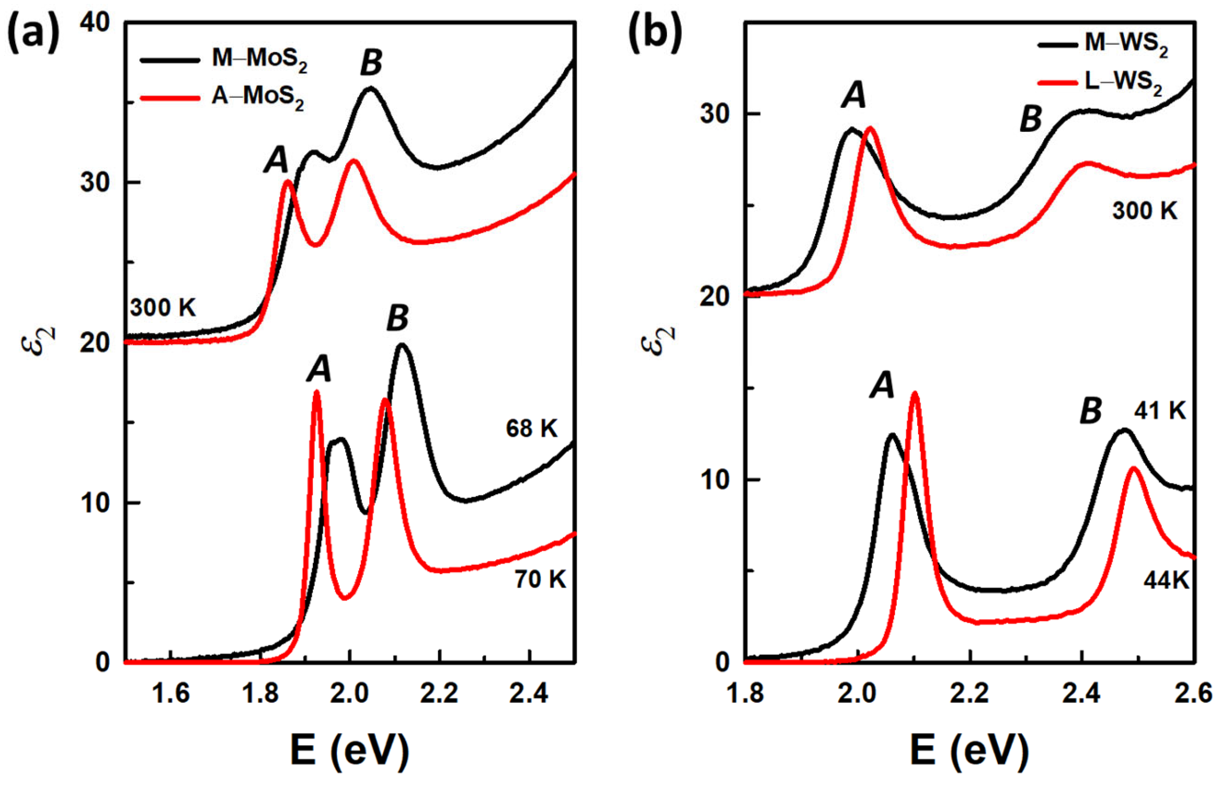
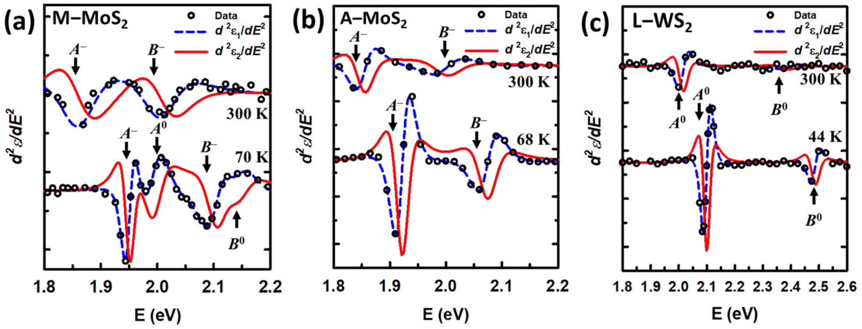
3.1. Analysis of <ɛ>

The pseudodielectric function <ɛ> spectra of the sample obtained by SE contain information of both the monolayers and the substrate. Therefore, a three-phase optical model including ambient/a TMDC monolayer/sapphire substrate was employed to extract the dielectric functions of the monolayers. Conventional approaches typically construct the dielectric functions of thin films using standard analytical functions such as Tauc–Lorentz, Lorentz, or Gaussian oscillators for each transition peak. However, in this work, the spectra measured at different temperatures are only slightly different from each other, making it difficult to trace using standard oscillators. Therefore, a higher-accuracy fitting method is required to preserve all the information of both real and imaginary parts of the dielectric functions for the second derivative analysis to be performed later in this study. Based on this issue, we employed a point-by-point fitting approach where the dielectric functions of the monolayers, including both the real and imaginary parts of ɛ, are obtained at each wavelength. In this approach, we fixed the thickness of MoS2 and WS2 monolayers at 0.7 and 0.8 nm, respectively [27,39,40]. Even if the surface roughness layer was not included in the optical model, the imaginary part of the dielectric function of all of the samples effectively resulted in a zero value below the bandgap region. This indicates the high quality and uniformity of the monolayers studied in this work. This also helps to reduce the number of free parameters required to describe the data.
Using this analysis approach, we extracted the dielectric functions of the M−MoS2, A−MoS2, M−WS2, and L−WS2 monolayers at each temperature, ranging from the lowest (68 K, 70 K, 41 K, and 44 K, respectively) to 300 K. The imaginary parts of the dielectric function of the mentioned monolayers are presented in Figure 2a–d for M−MoS2, A−MoS2, M−WS2, and L−WS2, respectively, at various temperatures. The spectra are offset by an increment of 15. At low temperatures, the critical point (CP) structures are blue-shifted and enhanced, with the appearance of new small CPs. These changes can be attributed to a significant reduction in electron–phonon interaction and the decrease in the lattice constant of TMDC materials at low temperatures, as figured out in Refs. [41,42]. Except for the A and B excitons, which will be discussed more thoroughly in this work, the data for the CPs (C, EI, EII, EIII, EIV, and EV) in the MoS2 monolayers and CPs (E0, C, E0 + Δ0, EIEVII) in the WS2 monolayers, including their energies and identification on band structure, are in good agreement with previous work, and so are not discussed further [26,27]. A comparison of imaginary parts of the dielectric function of monolayers MoS2 and WS2 at low temperatures and at 300 K on full scale are presented in Figure S3. Besides, while CP structures become sharper with a reduction in temperature, CP structures are also observed to be sharper in the monolayers fabricated by APCVD (A−MoS2) and LPCVD (L−WS2) compared to their counterparts. This observation suggests better crystallization formed in the monolayers grown by the mentioned methods. It might come from the fact that APCVD/LPCVD samples usually have larger domain sizes (typically can be up to 50 µm) compared to those of MOCVD samples (typically up to 1 µm), as reported for various samples in Refs. [43,44].
In this work, we focused on the behaviors of the A and B excitons from each monolayer as a function of temperature and fabrication method. These excitons are well known to occur at energy ranges from 1.5 to 2.5 eV and from 1.8 to 2.6 eV for MoS2 and WS2 monolayers, respectively. For better comparison of the excitons at room and low temperatures, we replotted the ɛ2 spectra in Figure 3a,b for MoS2 monolayers and WS2 monolayers, respectively, with the upper spectra for 300 K and lower ones at the lowest temperatures. The structures in the ɛ2 spectra of all the monolayers shift to lower energy and decrease in amplitude as the temperature increases. We also observed the structures of M−MoS2 and M−WS2 show clear separation of the A and B excitonic peaks and are strongly asymmetric at low temperatures. In fact, M−WS2 A and B excitonic structures consist of negatively charged and neutral exciton peaks with the charged ones being dominant, as indicated in Ref. [27]. Meanwhile, A−MoS2 and L−WS2 show relatively sharp structures with no sign of peak separation. Measurements and analyses of the samples at low temperatures helped to reduce thermal effects, therefore allowing for more precise information on the excitonic states. This structure sharpening and separation cannot be observed in room temperature spectra, emphasizing the importance of measurements at cryostat temperatures. Even though reduced thermal noise allows for the separation of peaks at low temperatures, the exciton energies and structures cannot be qualitatively determined by simply inspecting the original spectra, as the exciton structures are notably asymmetric due to contributions from transitions across various regions of the Brillouin zone. Therefore, we employed a standard procedure to determine CP energies at different temperatures by analyzing the second derivatives of the ɛ spectra.

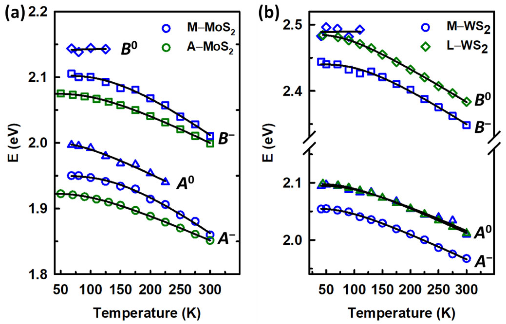
3.2. Exciton Energies

Exciton structures are usually hidden by overlapping and thermal noise. To resolve overlapped structures better even at low temperatures, second-derivative spectra, d 2 ε 1 d E 2 and d 2 ε 2 d E 2 , were obtained using the Savitzky and Golay method for differentiation and appropriate smoothening [45]. The spectra were fit to a standard analytical CP expression [46]:
d 2 ε d ω 2 = n n 1 A a m p e i ϕ ω E + i Γ n 2 , n 0 , = A a m p e i ϕ ω E + i Γ 2 ,       n = 0 ,
where a CP is represented by the amplitude Aamp, threshold energy E, broadening Γ, and phase ϕ as adjustable parameters. The exponent n has the values −1, −1/2, 0, and +1/2 for excitonic, 1, 2 (logarithmic), and 3D CPs, respectively. Both real and imaginary parts were fit simultaneously, and all the excitons were best fit with the n = −1 [26,27,47].
Figure 4a–c show the derivatives with their best fits for M−MoS2, A−MoS2, and L−WS2, respectively. The data of M−WS2 can be found in previous work [27]. Open circles represent the measured d 2 ε 1 d E 2 , while the dashed and the solid lines are the best fits to d 2 ε 1 d E 2   and d 2 ε 2 d E 2 , respectively. The number of data points is reduced and the data for d 2 ε 2 d E 2 are not shown for clarity. The spectra are offset by increments of 40,000. The blue-shift of CP energies and sharpening of the CP structures are clearly observed as the temperature decreases in all of the samples in Figure 4. The sharpening at low temperatures also helps to reveal the peak separation in M−MoS2 in the energy range of 1.8 to 2.2 eV.
The exciton energies of the monolayers determined at the lowest measured temperatures and at 300 K are listed in Table 1. In the room temperature MoS2 case, only two CPs at 1.86 and 2.01 are identified as A and B excitonic peaks. However, at 68 K, in addition to the blue-shift, these two CPs are separated into four CPs at 1.95, 2.00, 2.10, and 2.14 eV, being identified as A A0, B, and B0, respectively. This identification agrees well with the binding energy of MoS2 (the energy required to separate an electron from its associated hole within an exciton), which is near 40 meV [12,48]. It is interesting to note that even with the second derivative analysis at low temperatures, no peak separation was found in A−MoS2 and L−WS2, in contrast to that of M−MoS2 in this work and M−WS2 in previous work [26]. The A and B exciton values of A−MoS2 are closely related to those of charged excitons in M−MoS2, while the A and B exciton energies of L−WS2 are as similar as those of M−WS2, leading to identification of these excitons as AB for A−MoS2 and A0B0 for L−WS2. It means that for A−MoS2 and M−MoS2, trions can be found at all the temperatures, while for L−WS2, trions cannot be found even at the lowest temperature; for M−WS2, the A trion can be found at all the temperatures and the B trion vanished at temperatures above 150 K. In a recent work by Zhu et al. [28], the authors measured MoS2 and WS2 monolayers by SE and reported transition energies of excitons AB located at 1.88–2.00 eV for MoS2 and 2.02–2.40 eV for WS2. The origin of the excitons can hardly be identified due to the existence of only a single A and a single B peak. In comparison to the results obtained in this work (Table 1), A and B excitons of MoS2 monolayers might be recognized as trions, while A and B excitons of WS2 monolayers are neutral excitons. The temperature dependences of these excitons are presented in the next part, strengthening their identification of the origin.

3.3. Temperature Dependence

By applying second-derivative analysis to the spectra at all of the temperatures, the exciton energy values are obtained, as shown in Figure 5a,b for the MoS2 and WS2 samples, respectively. The data for M−WS2 are from Ref. [27]. The temperature dependence of the exciton data of A, B, and A0 of A−MoS2, M−MoS2, and M−WS2, and A0 and B0 of L−WS2 are presented by fit results (solid lines) of the CP data to a phenomenological expression that contains the Bose–Einstein statistical factor for phonons [47,49]:
E ( T ) = E B a B 1 + 2 e Θ / T 1
where Θ describes the mean frequency of the phonon and aB the interaction strength between electrons and phonons. The mean phonon frequency indicates how large the contribution of the acoustic phonons is. In this model, the electron–phonon interactions are responsible for the shrinkage in the bandgap with an increase in temperature. The details of the theoretical model for the electronic band structure and phonon dispersion can be found in Ref. [31]. For the other exciton, which has negligible curvature (possibly due to the limited data), a linear equation [47,49] was applied:
E T = E L λ T
where EL is an adjustable parameter, while λ is the temperature coefficient −dE/dT. The best fit parameters are listed in Table 2.
In Figure 5a, the behaviors of the A and B excitons of MoS2 monolayers with temperature show a similar tendency, which certifies that their origins are related. The excitons of A−MoS2 follow the Bose–Einstein expression well, confirming the existence of single A and single B excitons even at low temperatures. By using second-derivative analysis and temperature-dependence fitting, we can confirm these excitons are A and B charged excitons, which originate from negatively charged trions consisting of two electrons and one hole. The positions of these excitons are slightly red-shifted at all temperatures relative to those of M−MoS2. However, the separation of these excitons (spin-orbit splitting at maximum valence band at K valley) of A−MoS2 remains at 150 meV, which is the same value as that of M−MoS2 and agrees well with previous reports [50,51]. The fact that the fabricated A−MoS2 shows strongly trion-dominant behavior with no existence of neutral exciton peaks, while M−MoS2 shows trion-dominant with a separation of neutral-charged exciton peaks at low temperatures (below 250 K for A0 and below 150 K for B0), might relate to an influence of defect densities and impurities of the samples and/or differences in the local built-in strain originating from different growth methods.
It should be noted that, without careful experiments and analysis by temperature dependence, it is impossible to determine the origin of the excitonic peaks of A−MoS2 and M−MoS2, since each sample contains only single A and B peaks at relatively close energies in room-temperature measurements. The energy difference between A0 and A (trion binding energy) appears to be temperature-independent and remains constant at ~45 meV for MoS2. This value is in good agreement with the calculation of 43 meV by Matthias Drüppel et al. [13]. In MoS2, negative trions are commonly observed due to high electron density, which is often doped unintentionally, originating from sulfur vacancies, and too substantial to be fully neutralized by electronic back-gating of substrates. These excess electrons facilitate the formation of trions by binding with excitons, resulting in a significant number of trions even at room temperature [52].
The temperature dependences of the excitonic peaks of L−WS2 are presented in Figure 5b, in comparison to that of M−WS2 from the previous work [27]. In contrast to the excitonic behavior of A−MoS2 and M−MoS2 in this work, and M−WS2 in the previous work, which are all trion-dominant, L−WS2 shows single excitonic peak for each A and B exciton at the energies coinciding with those of A0 and B0 of M−WS2. In the previous work for M−WS2, due to peak separation, one can easily recognize the origin of each of the four excitons A, A0, B, and B0. With increasing temperature, the A and B excitons remain dominant, while the A0 structure decreases rapidly and B0 quickly vanished above ~150 K. They are thus hardly recognizable without a temperature study.
A and B excitons for L−WS2 in this work show total dominance of neutral exciton peaks without recognizable separation of trion structures even at cryogenic temperatures. The spin-orbit splitting of L−WS2 in this work remains at 382 meV, similar to that reported in Ref. [27]. The dominance of the neutral excitons of L−WS2 in this work, as opposed to the trion dominance of M−WS2 reported in the previous work, may come from differences in fabrication approaches leading to significantly sharper exciton peaks and fewer structural defects, which are a well-known source of trion formations, as depicted previously [14,53,54]. It is noteworthy that the B0 exciton in the previous work could not be properly fitted due to lack of data after 120 K. This has now been addressed in this work. Last but not least, the knowledge of the thermo-optic properties of TMDC monolayers acquired in this work would be helpful in designing all-optical switch devices [55,56].

4. Conclusions

We present a comparison study of the optical properties of MoS2 monolayers grown using MOCVD (M−MoS2) and APCVD (A−MoS2), and WS2 monolayers fabricated using MOCVD (M−WS2) and LPCVD (L−WS2). The monolayers were measured by SE at temperatures from cryogenic to 300 K in an energy range from 1.5 to 6.0 eV. The excitonic energies at each temperature were studied by fitting the second derivatives of the obtained spectra to a standard analytical CP expression to identify and separate the structures at various temperatures. While the MOCVD monolayers clearly show the formation and separation of exciton (A0 and B0) and trion (A and B) peaks with trion-dominant behavior, in A−MoS2 and L−WS2 we found only single A and B peaks. The A−MoS2 monolayer was identified as trion-dominant and the L−WS2 monolayer was identified as neutral exciton-dominant as a result of the data presented here.

Supplementary Materials

The following supporting information can be downloaded at: https://www.mdpi.com/article/10.3390/ma17225455/s1, Figure S1: Optical images of the monolayers (a) M−MoS2, (b) A−MoS2, and (c) L−WS2 on sapphire substrate.; Figure S2: Measured Ψ and Δ of monolayer M−WS2 at various spots by focused beam SE.; Figure S3: Imaginary parts of dielectric function of monolayers (a) MoS2 and (b) WS2 at low temperature and at 300 K.

Author Contributions

Conceptualization, methodology, investigation, writing—review and editing, H.T.N.; data curation, investigation, writing—original draft preparation, X.A.N.; Sample preparation and validation, A.T.H.; Conceptualization, validation, supervision T.J.K. All authors have read and agreed to the published version of the manuscript.

Funding

This research was funded by the Vietnam Academy of Science and Technology, grant number THTETN.05/22-23. The work in KHU was supported by a National Research Foundation of Korea (NRF) grant funded by the Korean government (MSIP) (NRF-2020R1A5A1016518) and by a grant from Kyung Hee University in 2023 (KHU-20233265).

Institutional Review Board Statement

Not applicable.

Informed Consent Statement

Not applicable.

Data Availability Statement

The original contributions presented in the study are included in the article/Supplementary Material, further inquiries can be directed to the corresponding authors.

Conflicts of Interest

The authors declare no conflicts of interest.

References

  1. Joseph, S.; Mohan, J.; Lakshmy, S.; Thomas, S.; Chakraborty, B.; Thomas, S.; Kalarikkal, N. A review of the synthesis, properties, and applications of 2D transition metal dichalcogenides and their heterostructures. Mater. Chem. Phys. 2023, 297, 127332. [Google Scholar] [CrossRef]
  2. Wang, Q.H.; Kalantar-Zadeh, K.; Kis, A.; Coleman, J.N.; Strano, M.S. Electronics and optoelectronics of two-dimensional transition metal dichalcogenides. Nat. Nanotechnol. 2012, 7, 699–712. [Google Scholar] [CrossRef]
  3. Lee, Y.-C.; Chang, S.-W.; Chen, S.-H.; Chen, S.-L.; Chen, H.-L. Optical Inspection of 2D Materials: From Mechanical Exfoliation to Wafer-Scale Growth and Beyond. Adv. Sci. 2022, 9, 2102128. [Google Scholar] [CrossRef] [PubMed]
  4. Chen, P.; Lo, T.W.; Fan, Y.; Wang, S.; Huang, H.; Lei, D. Chiral coupling of valley excitons and light through photonic spin–orbit interactions. Adv. Opt. Mater. 2020, 8, 1901233. [Google Scholar] [CrossRef]
  5. Chaves, A.; Azadani, J.G.; Alsalman, H.; Da Costa, D.; Frisenda, R.; Chaves, A.; Song, S.H.; Kim, Y.D.; He, D.; Zhou, J. Bandgap engineering of two-dimensional semiconductor materials. NPJ 2D Mater. Appl. 2020, 4, 29. [Google Scholar] [CrossRef]
  6. Seravalli, L.; Bosi, M. A review on chemical vapour deposition of two-dimensional MoS2 flakes. Materials 2021, 14, 7590. [Google Scholar] [CrossRef]
  7. Mouloua, D.; Kotbi, A.; Deokar, G.; Kaja, K.; El Marssi, M.; El Khakani, M.A.; Jouiad, M. Recent progress in the synthesis of MoS2 thin films for sensing, photovoltaic and plasmonic applications: A review. Materials 2021, 14, 3283. [Google Scholar] [CrossRef]
  8. Vidya, C.; Manjunatha, C.; Pranjal, A.; Faraaz, I.; Prashantha, K. A multifunctional nanostructured molybdenum disulphide (MoS2): An overview on synthesis, structural features, and potential applications. Mater. Res. Innov. 2023, 27, 177–193. [Google Scholar] [CrossRef]
  9. Lan, C.; Li, C.; Ho, J.C.; Liu, Y. 2D WS2: From vapor phase synthesis to device applications. Adv. Electron. Mater. 2021, 7, 2000688. [Google Scholar] [CrossRef]
  10. Yoo, S.; Park, Q.-H. Spectroscopic ellipsometry for low-dimensional materials and heterostructures. Nanophotonics 2022, 11, 2811–2825. [Google Scholar] [CrossRef]
  11. Voshell, A.; Terrones, M.; Rana, M. Review of optical properties of two-dimensional transition metal dichalcogenides. Wide Bandgap Power Energy Devices Appl. III 2018, 10754, 66–83. [Google Scholar]
  12. Golovynskyi, S.; Datsenko, O.I.; Dong, D.; Lin, Y.; Irfan, I.; Li, B.; Lin, D.; Qu, J. Trion binding energy variation on photoluminescence excitation energy and power during direct to indirect bandgap crossover in monolayer and few-layer MoS2. J. Phys. Chem. C 2021, 125, 17806–17819. [Google Scholar] [CrossRef]
  13. Drüppel, M.; Deilmann, T.; Krüger, P.; Rohlfing, M. Diversity of trion states and substrate effects in the optical properties of an MoS2 monolayer. Nat. Commun. 2017, 8, 2117. [Google Scholar] [CrossRef] [PubMed]
  14. Chowdhury, T.; Paul, D.; Nechiyil, D.; Gokul, M.A.; Watanabe, K.; Taniguchi, T.; Kumar, G.V.P.; Rahman, A. Modulation of trion and exciton formation in monolayer WS2 by dielectric and substrate engineering. 2D Mater. 2021, 8, 045032. [Google Scholar] [CrossRef]
  15. Li, X.; Yang, J.; Sun, H.; Huang, L.; Li, H.; Shi, J. Controlled Synthesis and Accurate Doping of Wafer-Scale 2D Semiconducting Transition Metal Dichalcogenides. Adv. Mater. 2023, 2305115. [Google Scholar] [CrossRef]
  16. Jin, Y.; Yu, K. A review of optics-based methods for thickness and surface characterization of two-dimensional materials. J. Phys. D Appl. Phys. 2021, 54, 393001. [Google Scholar] [CrossRef]
  17. Fujiwara, H. Spectroscopic Ellipsometry: Principles and Applications; John Wiley & Sons: Hoboken, NJ, USA, 2007. [Google Scholar]
  18. Aspnes, D. Spectroscopic ellipsometry—Past, present, and future. Thin Solid Film. 2014, 571, 334–344. [Google Scholar] [CrossRef]
  19. Jellison, G.E. Data analysis for spectroscopic ellipsometry. In Handbook of Ellipsometry; Springer: Berlin/Heidelberg, Germany, 2005; pp. 237–296. [Google Scholar]
  20. Liu, H.-L.; Shen, C.-C.; Su, S.-H.; Hsu, C.-L.; Li, M.-Y.; Li, L.-J. Optical properties of monolayer transition metal dichalcogenides probed by spectroscopic ellipsometry. Appl. Phys. Lett. 2014, 105, 201905. [Google Scholar] [CrossRef]
  21. Luria, O.; Mohapatra, P.K.; Patsha, A.; Kribus, A.; Ismach, A. Large-scale characterization of two-dimensional monolayer MoS2 island domains using spectroscopic ellipsometry and reflectometry. Appl. Surf. Sci. 2020, 524, 146418. [Google Scholar] [CrossRef]
  22. Iqbal, M.W.; Shahzad, K.; Akbar, R.; Hussain, G. A review on Raman finger prints of doping and strain effect in TMDCs. Microelectron. Eng. 2020, 219, 111152. [Google Scholar] [CrossRef]
  23. Al-Ani, I.A.; As’ham, K.; Klochan, O.; Hattori, H.T.; Huang, L.; Miroshnichenko, A.E. Recent advances on strong light-matter coupling in atomically thin TMDC semiconductor materials. J. Opt. 2022, 24, 053001. [Google Scholar] [CrossRef]
  24. Hu, Z.; Wu, Z.; Han, C.; He, J.; Ni, Z.; Chen, W. Two-dimensional transition metal dichalcogenides: Interface and defect engineering. Chem. Soc. Rev. 2018, 47, 3100–3128. [Google Scholar] [CrossRef] [PubMed]
  25. Xiong, Z.; Zhong, L.; Wang, H.; Li, X. Structural defects, mechanical behaviors, and properties of two-dimensional materials. Materials 2021, 14, 1192. [Google Scholar] [CrossRef] [PubMed]
  26. Park, H.G.; Kim, T.J.; Kim, H.S.; Yoo, C.H.; Barange, N.S.; Le, V.L.; Kim, H.U.; Senthilkumar, V.; Le, C.T.; Kim, Y.S.; et al. Temperature dependence of the critical points of monolayer MoS2 by ellipsometry. Appl. Spectrosc. Rev. 2016, 51, 621–635. [Google Scholar] [CrossRef]
  27. Nguyen, H.T.; Kim, T.J.; Park, H.G.; Le, V.L.; Nguyen, X.A.; Koo, D.; Lee, C.-H.; Cuong, D.D.; Hong, S.C.; Kim, Y.D. Temperature dependence of optical properties of monolayer WS2 by spectroscopic ellipsometry. Appl. Surf. Sci. 2020, 511, 145503. [Google Scholar] [CrossRef]
  28. Zhu, X.; He, J.; Zhang, R.; Cong, C.; Zheng, Y.; Zhang, H.; Zhang, S.; Chen, L. Effects of dielectric screening on the excitonic and critical points properties of WS2/MoS2 heterostructures. Nanoscale 2020, 12, 23732–23739. [Google Scholar] [CrossRef]
  29. Nguyen, X.A.; Le, L.V.; Kim, S.H.; Kim, Y.D.; Diware, M.S.; Kim, T.J.; Kim, Y.D. Temperature dependence of the dielectric function and critical points of monolayer WSe2. Sci. Rep. 2024, 14, 13486. [Google Scholar] [CrossRef]
  30. Park, H.G.; Kim, T.J.; Ullah, F.; Le, V.L.; Nguyen, H.T.; Kim, Y.S.; Kim, Y.D. Temperature dependence of the dielectric function of monolayer MoSe2. Sci. Rep. 2018, 8, 3173. [Google Scholar] [CrossRef]
  31. Liu, H.-L.; Yang, T.; Chen, J.-H.; Chen, H.-W.; Guo, H.; Saito, R.; Li, M.-Y.; Li, L.-J. Temperature-dependent optical constants of monolayer MoS2, MoSe2, WS2, and WSe2: Spectroscopic ellipsometry and first-principles calculations. Sci. Rep. 2020, 10, 15282. [Google Scholar] [CrossRef]
  32. Kravets, V.; Prorok, V.; Poperenko, L.; Shaykevich, I. Ellipsometry and optical spectroscopy of low-dimensional family TMDs. Semicond. Phys. Quantum Electron. Optoelectron. 2017, 20, 284–296. [Google Scholar] [CrossRef]
  33. Zhu, X.; Li, D.; Zhang, R.; Zhang, H.; Cong, C.; Zhu, M.; Shi, Y.; Wu, Y.; Wang, S.; Zheng, Y. Probing quantum confinement effects on the excitonic property and electronic band structures of MoS2. Appl. Surf. Sci. 2020, 519, 146262. [Google Scholar] [CrossRef]
  34. Elliott, J.D.; Xu, Z.; Umari, P.; Jayaswal, G.; Chen, M.; Zhang, X.; Martucci, A.; Marsili, M.; Merano, M. Surface susceptibility and conductivity of MoS 2 and WSe 2 monolayers: A first-principles and ellipsometry characterization. Phys. Rev. B 2020, 101, 045414. [Google Scholar] [CrossRef]
  35. Hoang, A.T.; Hu, L.; Kim, B.J.; Van, T.T.N.; Park, K.D.; Jeong, Y.; Lee, K.; Ji, S.; Hong, J.; Katiyar, A.K.; et al. Low-temperature growth of MoS2 on polymer and thin glass substrates for flexible electronics. Nat. Nanotechnol. 2023, 18, 1439–1447. [Google Scholar] [CrossRef]
  36. Tao, L.; Li, H.; Gao, Y.; Chen, Z.; Wang, L.; Deng, Y.; Zhang, J.; Xu, J.B. Deterministic and Etching—Free Transfer of Large—Scale 2D Layered Materials for Constructing Interlayer Coupled van der Waals Heterostructures. Adv. Mater. Technol. 2018, 3, 1700282. [Google Scholar] [CrossRef]
  37. McCreary, K.M.; Hanbicki, A.T.; Sivaram, S.V.; Jonker, B.T. A-and B-exciton photoluminescence intensity ratio as a measure of sample quality for transition metal dichalcogenide monolayers. APL Mater. 2018, 6, 111106. [Google Scholar] [CrossRef]
  38. Shi, Z.; Wang, X.; Sun, Y.; Li, Y.; Zhang, L. Interlayer coupling in two-dimensional semiconductor materials. Semicond. Sci. Technol. 2018, 33, 093001. [Google Scholar] [CrossRef]
  39. Nourbakhsh, A.; Zubair, A.; Sajjad, R.N.; Tavakkoli KG, A.; Chen, W.; Fang, S.; Ling, X.; Kong, J.; Dresselhaus, M.S.; Kaxiras, E. MoS2 field-effect transistor with sub-10 nm channel length. Nano Lett. 2016, 16, 7798–7806. [Google Scholar] [CrossRef]
  40. Najmaei, S.; Liu, Z.; Ajayan, P.; Lou, J. Thermal effects on the characteristic Raman spectrum of molybdenum disulfide (MoS2) of varying thicknesses. Appl. Phys. Lett. 2012, 100, 013106. [Google Scholar] [CrossRef]
  41. Murray, R.; Evans, B. The thermal expansion of 2H-MoS2 and 2H-WSe2 between 10 and 320 K. J. Appl. Crystallogr. 1979, 12, 312–315. [Google Scholar] [CrossRef]
  42. Mitioglu, A.; Galkowski, K.; Surrente, A.; Klopotowski, L.; Dumcenco, D.; Kis, A.; Maude, D.K.; Plochocka, P. Magnetoexcitons in large area CVD-grown monolayer MoS2 and MoSe2 on sapphire. Phys. Rev. B 2016, 93, 165412. [Google Scholar] [CrossRef]
  43. Hoang, A.T.; Qu, K.; Chen, X.; Ahn, J.-H. Large-area synthesis of transition metal dichalcogenides via CVD and solution-based approaches and their device applications. Nanoscale 2021, 13, 615–633. [Google Scholar] [CrossRef] [PubMed]
  44. Lee, D.H.; Sim, Y.; Wang, J.; Kwon, S.-Y. Metal–organic chemical vapor deposition of 2D van der Waals materials—The challenges and the extensive future opportunities. Apl Mater. 2020, 8, 030901. [Google Scholar] [CrossRef]
  45. Savitzky, A.; Golay, M.J.E. Smoothing and differentiation of data by simplified least squares procedures. Anal. Chem. 1964, 36, 1627–1639. [Google Scholar] [CrossRef]
  46. Cardona, M. Modulation Spectroscopy; Academic Press: Cambridge, MA, USA, 1969. [Google Scholar]
  47. Kim, T.J.; Hwang, S.Y.; Byun, J.S.; Diware, M.S.; Choi, J.; Park, H.G.; Kim, Y.D. Temperature dependence of the dielectric functions and the critical points of InSb by spectroscopic ellipsometry from 31 to 675 K. J. Appl. Phys. 2013, 114, 103501. [Google Scholar]
  48. Pei, J.; Yang, J.; Xu, R.; Zeng, Y.H.; Myint, Y.W.; Zhang, S.; Zheng, J.C.; Qin, Q.; Wang, X.; Jiang, W. Exciton and trion dynamics in bilayer MoS2. Small 2015, 11, 6384–6390. [Google Scholar] [CrossRef]
  49. Lautenschlager, P.; Garriga, M.; Cardona, M. Temperature dependence of the interband critical-point parameters of InP. Phys. Rev. B 1987, 36, 4813. [Google Scholar] [CrossRef]
  50. Roch, J.G.; Froehlicher, G.; Leisgang, N.; Makk, P.; Watanabe, K.; Taniguchi, T.; Warburton, R.J. Spin-polarized electrons in monolayer MoS2. Nat. Nanotechnol. 2019, 14, 432–436. [Google Scholar] [CrossRef]
  51. Khan, M.; Leuenberger, M.N. Room-temperature superparamagnetism due to giant magnetic anisotropy in MoS defected single-layer MoS2. J. Phys. Condens. Matter 2018, 30, 155802. [Google Scholar] [CrossRef]
  52. Goswami, T.; Rani, R.; Hazra, K.S.; Ghosh, H.N. Ultrafast Carrier Dynamics of the Exciton and Trion in MoS2 Monolayers Followed by Dissociation Dynamics in Au@MoS2 2D Heterointerfaces. J. Phys. Chem. Lett. 2019, 10, 3057–3063. [Google Scholar] [CrossRef]
  53. Sebait, R.; Biswas, C.; Song, B.; Seo, C.; Lee, Y.H. Identifying defect-induced trion in monolayer WS2 via carrier screening engineering. ACS Nano 2021, 15, 2849–2857. [Google Scholar] [CrossRef]
  54. Hossen, M.F.; Shendokar, S.; Aravamudhan, S. Defects and Defect Engineering of Two-Dimensional Transition Metal Dichalcogenide (2D TMDC) Materials. Nanomaterials 2024, 14, 410. [Google Scholar] [CrossRef] [PubMed]
  55. Torres-Torres, C.; Perea-López, N.; Elías, A.L.; Gutiérrez, H.R.; Cullen, D.A.; Berkdemir, A.; López-Urías, F.; Terrones, H.; Terrones, M. Third order nonlinear optical response exhibited by mono-and few-layers of WS2. 2d Mater. 2016, 3, 021005. [Google Scholar] [CrossRef]
  56. Wu, K.; Guo, C.; Wang, H.; Zhang, X.; Wang, J.; Chen, J. All-optical phase shifter and switch near 1550nm using tungsten disulfide (WS2) deposited tapered fiber. Opt. Express 2017, 25, 17639–17649. [Google Scholar] [CrossRef] [PubMed]
Figure 1. Typical Raman and PL spectra of MoS2 monolayer (a,b) and WS2 monolayer (c,d) samples performed with 532 nm laser excitation under ambient conditions. M-, L-, and A- stand for MOCVD, LPCVD, and APCVD fabrication methods, respectively.
Materials 17 05455 g001
Figure 2. Imaginary parts of the dielectric function of (a) M−MoS2, (b) A−MoS2, (c) M−WS2, and (d) L−WS2 monolayers from 68 K, 70 K, 41 K, and 44 K, respectively, to 300 K. The spectra are offset by an increment of 15 for clarity.
Materials 17 05455 g002
Figure 3. Imaginary parts of the dielectric function of monolayers (a) MoS2 and (b) WS2 at low temperatures and at 300 K on expanded scale around the regions of the A and B excitonic peaks.
Materials 17 05455 g003
Figure 4. The best fit for d 2 ε 1 d E 2   (dashed line) and d 2 ε 2 d E 2 (solid line) from 1.8 to 2.2 eV for M−MoS2 (a) and A−MoS2 (b), and from 1.8 to 2.6 eV for L−WS2 (c). The data at each range is appropriately multiplied and the data for d 2 ε 2 d E 2 (open circles) are not shown for clarity.
Materials 17 05455 g004
Figure 5. Temperature dependence of the CP energies (open symbols) and the best fit (solid lines) for excitons of (a) MoS2 monolayers and (b) WS2 monolayers. The data for M−WS2 are from Ref. [27].
Materials 17 05455 g005
Table 1. Exciton energies at the lowest measured temperature and at 300 K of the monolayers.
Exciton EnergiesA−MoS2M−MoS2L−WS2M−WS2 1
70 K300 K68 K300 K44 K300 K41 K300 K
A1.92 ± 0.011.85 ± 0.031.95 ± 0.011.86 ± 0.03----2.05 ± 0.011.96 ± 0.02
A0----2.00 ± 0.02--2.10 ± 0.022.01 ± 0.022.09 ± 0.012.00 ± 0.02
B2.08 ± 0.022.00 ± 0.042.10 ± 0.012.01 ± 0.02----2.44 ± 0.012.34 ± 0.02
B0----2.14 ± 0.02--2.48 ± 0.012.38 ± 0.042.48 ± 0.02--
1 Data from Ref. [27].
Table 2. The best-fitting parameters of the temperature dependences of the CPs of the monolayers.
SampleExcitonEB (eV)aB (meV)Θ (K)EL (eV)λ (10−4 eVK−1)
A−MoS2A1.99 ± 0.0167 ± 3318 ± 8----
B2.16 ± 0.0187 ± 5361 ± 12----
M−MoS2A2.14 ± 0.03191 ± 33505 ± 42----
A02.06 ± 0.0360 ± 34249 ± 93----
B2.28 ± 0.03186 ± 36488 ± 47----
B0------2.14 ± 0.010.26 ± 0.01
L−WS2A02.17 ± 0.0169 ± 3287 ± 9----
B02.56 ± 0.0373 ± 4267 ± 9----
M−WS2 1A2.11 ± 0.0163 ± 6266 ± 17----
A02.16 ± 0.0273 ± 22314 ± 59----
B2.55 ± 0.02112 ± 23374 ± 42----
B0------2.49 ± 0.010.10 ± 0.01
1 Data from Ref. [27].
Disclaimer/Publisher’s Note: The statements, opinions and data contained in all publications are solely those of the individual author(s) and contributor(s) and not of MDPI and/or the editor(s). MDPI and/or the editor(s) disclaim responsibility for any injury to people or property resulting from any ideas, methods, instructions or products referred to in the content.

