Abstract
To maximize the photoelectrochemical (PEC) hydrogen production performance of quantum dot (QD)-decorated photoelectrodes, it is crucial to prioritize the optimization of electrode’s structure, including thickness and porosity. In this study, we prepare PbS QD-decorated mesoporous TiO2 photoanodes for PEC hydrogen production, and systematically investigate the influence of the photoanode thickness on optical properties and PEC performances. As the thickness of photoanodes increases from 6.4 µm to 16.3 µm, the light absorption capability is enhanced across the entire visible and near-infrared (IR) spectrum due to the improved loading of PbS QDs. However, the photocurrent density is optimized for the 11.9 µm thick photoanode (15.19 mA/cm2), compared to the 6.4 µm thick (10.80 mA/cm2) and 16.3 µm thick photoanodes (11.93 mA/cm2). This optimization is attributed to the trade-off between the light absorption capability and the efficient mass transfer of the electrolyte as the photoanode thickness increases, which is confirmed by the lowest charge transfer resistance (Rct) evaluated from the electrochemical impedance data.
1. Introduction
To effectively address the rapidly increasing energy demand and the threat of global warming, the efficient utilization of clean and renewable energy is essential. Research aimed at maximizing the potential of solar energy is considered a key element in sustainable energy supply and climate change mitigation. One of the most promising approaches for the efficient utilization of solar energy and the generation of renewable and eco-friendly energy is photoelectrochemical (PEC) hydrogen production [1,2,3,4,5].
As light-absorbing materials utilized in solar energy devices, quantum dots (QDs) have garnered significant attention. QDs exhibit distinct electrical and optical properties because of the quantum confinement effect, differentiating them from bulk materials [6,7]. The unique optical characteristics of QDs, coupled with advantages such as multiple-exciton generation (MEG), high absorption coefficients, and facile bandgap control, have led to substantial interest in the research fields of solar cells and PEC hydrogen pro-duction [8,9,10,11].
Moreover, introducing the QDs with a relatively small band-gap (Eg < 1.5 eV) as photosensitizers allows for the effective utilization of incident light not only in the visible spectrum but even in the near-infrared range. In particular, PbS QDs can be effectively employed in PEC hydrogen production as the light-absorbing material because of their broad absorption spectrum and high quantum efficiency [12,13,14]. Studies have reported the enhancement of the light absorption spectrum and outstanding PEC hydrogen production performance by decorating PbS QDs on wide band-gap semiconductors like TiO2 and BiVO4 [15,16,17,18].
To maximize the PEC hydrogen production performance of such QD-decorated photoelectrodes, it is crucial to prioritize the optimization of the electrode’s structure, including thickness and porosity. As the thickness of the photoelectrode increases, it can absorb a larger quantity of photons per unit of active area. However, beyond a certain thickness, drawbacks such as increased electron recombination with the redox couple in the electrolyte and slowed mass transfer within the electrolyte may arise for photoelectrodes [19,20,21]. Therefore, it is necessary to investigate the influence of the thickness of QD-decorated photoanodes on the performance of PEC hydrogen production. For instance, in the field of QD-sensitized solar cells, sufficient research has been conducted on the variation and optimization of photovoltaic performances according to the thickness of photoelectrodes [22,23]. However, in the field of PEC hydrogen production, such research endeavors have been scarcely pursued, despite their fundamental necessity [24,25].
In this study, we coated PbS QDs onto the surface of mesoporous TiO2 films through successive ionic-layer adsorption and reaction (SILAR) process and optimized the thickness of the photoelectrode to maximize PEC hydrogen production performance. The morphologies and uniformity, as well as the chemical states of the PbS QDs on the TiO2 surface, were characterized. In addition, we systematically investigated the impact of the photoelectrode thickness on its optical properties and PEC hydrogen production characteristics. Additionally, we specifically explored the charge transfer properties depending on the photoelectrode thickness using electrochemical impedance analysis. Because of the superior optical properties of PbS QDs, including a wide absorption range as well as thickness optimization, the TiO2/PbS QD photoanode exhibited a remarkable photocurrent density of 15.19 mA/cm2 at 0.6 VRHE under the condition of 11.9 µm in thickness.
2. Materials and Methods
2.1. Preparation of Mesoporous TiO2 Film
Fluorine-doped tin oxide-coated (FTO) glass substrates (2.2 mm thickness, 8 Ω/sq, Pilkington, Tokyo, Japan) were used as the substrates for the photoelectrode. The FTO substrates were sequentially cleaned using acetone and ethanol in an ultrasonic cleaner (SD-B200H, MUJIGAE, Seoul, Republic of Korea). After cleaning, the substrates were treated with ultraviolet/ozone (UV/ozone cleaner, Yuil Ultra Violet System, YUILUV. Co., Ltd., Incheon, Republic of Korea) for 15 min to remove residual organic materials and moisture. On the cleaned FTO substrates, a solution of 7.5 wt% Ti(IV) bis(ethylacetoacetato)-diiso-propoxide (Aldrich, St Louis, MO, USA) dissolved in n-butanol (Daejung, Siheung, Republic of Korea) was spin-coated, followed by heat treatment at 450 °C for 10 min in a box-type furnace. A semi-transparent TiO2 paste (Ti-Nanoxide T/SP, SOLARONIX S.A, Aubonne, Switzerland) was coated on top of the pre-treated FTO substrate using a doctor blading method. The thickness of the TiO2 film was controlled by varying the number of layers (1 to 3 layers) of scotch tape attached during the doctor blading. The coated TiO2 film was then sintered by gradually increasing the temperature in the box-type furnace: 150 °C for 10 min, 250 °C for 10 min, 400 °C for 10 min, and finally 500 °C for 30 min in air.
2.2. Coating of PbS QDs on the Surface of Mesoporous TiO2 Film
To coat PbS QDs on the surface of mesoporous TiO2 film, the SILAR method was employed. Specifically, PbS QDs were coated by immersing the TiO2 film on FTO substrate in a methanol solution of 0.02 M Pb(NO3)2 (Aldrich) for 60 s, followed by immersion in a solution of 0.02 M Na2S (Aldrich) in DI water/methanol (1:1, v/v). This process was repeated for a total of 4 cycles. Subsequently, a zinc sulfide (ZnS) passivation layer was formed by repeating the SILAR process three times using a solution of 0.05 M Zn(Ac)2 (Aldrich) in ethanol (for 50 s), and a solution of 0.05 M Na2S in DI water/methanol (1:1, v/v) (for 50 s).
2.3. Characterization
The morphology of the PbS QD-coated TiO2 nanoparticles was confirmed by high-resolution transmission electron microscopy (HR-TEM; JEM-2010, JEOL, Tokyo, Japan). The cross-sectional structure of the fabricated photoelectrode was observed using scanning electron microscopy (SEM, S-4700, HITACHI, Tokyo, Japan). Elemental composition was analyzed using energy-dispersive X-ray spectroscopy (EDX) attached to an SEM (Bruker AXS Quantax 4010, HITACHI). The performance of the photoelectrode was measured using a three-electrode system consisting of the photoelectrode, Pt mesh, and Hg/HgO reference electrode in a quartz reactor containing an electrolyte composed of 0.25 M sodium sulfide pentahydrate (Daejung, Siheung, Republic of Korea) and 0.35 M sodium sulfite anhydrous (Daejung, Siheung, Republic of Korea) (pH~13). Impedance data, chronoamperometric curves, and photocurrent density–voltage (J–V) curves of the photoelectrode were analyzed using a potentiostat (M204, Autolab, Utrecht, The Netherlands). The light incident on the photoelectrode was generated using a 150 W xenon lamp (PEC-L01, Peccell, Yokohama, Japan) equipped with an AM 1.5 G filter. The light intensity was adjusted to 1 sun (100 mW/cm2) using a certified silicon reference solar cell. UV-vis transmittance spectra and absorption spectra of the TiO2/PbS/ZnS films were achieved using UV-vis spectroscopy (OPTIZEN 2120 UV, Mecasys, Daejeon, Republic of Korea). X-ray photoelectron spectroscopy (XPS, K-alph+, Thermofisher Scientific, E. Grinstead, UK) was used to confirm the surface chemical states of the TiO2/PbS/ZnS films. X-ray diffraction (XRD) analyses were carried out using an X-ray diffractometer (SmartLab 9 kW system, Rigaku, Tokyo, Japan). The evolved hydrogen was analyzed by gas chromatography (GC) (Chrozen GC System, YoungIn Chromass, Anyang, Republic of Korea).
3. Results and Discussion
Figure 1a,b show the HR-TEM images of PbS QD-coated TiO2 nanoparticles. After coating PbS QDs on the surface of the mesoporous TiO2 film via the SILAR method, the film was detached from the substrate for TEM analysis. It was confirmed that TiO2 nanoparticles, approximately 20 nm in size, were strongly and randomly bonded to each other through high-temperature annealing (Figure 1a). Particularly, the (200) lattice plane of galena PbS (fringe spacing~0.297 nm) [26] was identified in a highly magnified image (Figure 1b). Figure S1 presents the HR-TEM images displaying the morphology of the bare TiO2 nanoparticles. Figure S1a reveals a structural resemblance to that depicted in Figure 1a, suggesting the adsorption of PbS QDs onto the surface of TiO2 nanoparticles. The (101) lattice plane of anatase TiO2 (fringe spacing~0.353 nm) [27] is identified in Figure S1b. Figure S2 represents the HR-TEM images of the PbS QD-coated TiO2 nanoparticles. As shown in Figure S2, the average diameter of the PbS QDs is 4.81 ± 0.82 nm. The observed lattice fringe of 0.297 nm of PbS QDs that corresponds to the (200) plane, indicating the adsorption of PbS QDs over the TiO2 nanoparticles.
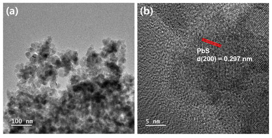
Figure 1.
(a) HR-TEM image of PbS QD-coated TiO2 nanoparticles, and (b) high-magnification image of (a).
Figure 2a–c shows SEM images and EDX spectra comparing TiO2/PbS/ZnS films with different thicknesses. As observed in the SEM images, the TiO2/PbS/ZnS films were coated with varying thicknesses between approximately 6 to 16 µm under each condition. The thickness of these films was controlled by varying the number of layers (one to three layers) of scotch tape attached during the doctor blading of the TiO2 paste. The thickness of each film was found to be 6.4 µm (Figure 2a), 11.9 µm (Figure 2b), and 16.3 µm (Figure 2c), respectively. At thicknesses beyond this point, poor adhesion between the TiO2 film and the FTO glass substrate led to the formation of cracks, making it difficult to fabricate a stable electrode. The bottom images and tables in Figure 2a–c represent the EDX spectra and the calculated atomic compositions of each electrode, implying the formation of PbS QDs and ZnS passivation layer on the surface of mesoporous TiO2 film. From the mapping images in Figure 2d,e, it can be noted that PbS QDs dots and ZnS passivation layer were uniformly and conformally deposited along the cross-section regardless of the thickness of the TiO2 film. These results indicate that the SILAR method we employed in this study is suitable for the coating of QDs and the passivation layer onto relatively thick mesoporous electrode surfaces. To investigate whether the coating of QDs influences the thickness of the TiO2 electrode, we also measured the thickness of the bare TiO2 electrode without QD coating (Figure S3). Depending on the number of layers, the thickness for each layer was determined to be 6.2 µm for a single layer (Figure S3a), 11.3 µm for two layers (Figure S3b), and 16.8 µm for three layers (Figure S3c). These values show only a minor difference within 1 µm compared to the electrode thickness after QD coating, which is considered to be within the expected margin of error associated with the Dr blading method for the TiO2 film deposition. Furthermore, the mapping presented in Figure 2d–f indicates that PbS QDs are coated within the pores of the TiO2 rather than forming an additional layer on the TiO2 film. In conclusion, it can be stated that the coating of QDs does not significantly affect the thickness of the electrode.
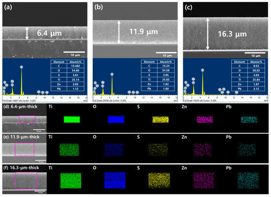
Figure 2.
(a–c) SEM images and EDX spectra for TiO2/PbS films according to the thickness. (d–f) EDX mapping for each element (Ti, O, S, Zn, Pb) of TiO2/PbS films.
Figure 3a is a graph analyzing XRD patterns to characterize the crystal structure and crystallinity of bare TiO2 and TiO2/PbS/ZnS films. For the XRD analysis, the 11.9 µm thick film was used. Multiple diffraction peaks observed at 25.3, 37.9, 48.1, 54.0, 55.1, 63.8, 68.9, 70.3 and 74.3 2θ degrees in the XRD pattern correspond to the (101), (004), (200), (105), (211), (204), (116), (220) and (107) crystal planes of TiO2 with an anatase phase [28,29,30,31,32,33]. Additionally, two diffraction peaks at 30.1 and 43.0 2θ degrees for the TiO2/PbS/ZnS film represent the (200) and (220) planes of PbS in the galena phase [34,35,36,37,38]. The Gaussian fitting for the (200) plane peak of PbS revealed a peak position at 30.2 2θ degrees and a full width at half maximum (FWHM) of approximately 1.75. The average crystallite size can be determined using Scherrer’s equation [39], which is shown in Equation (1):
where D represents the average crystallite size, λ is the X-ray wavelength (1.5406 Å), K is the dimensionless coefficient of particle shape (assumed to be 0.9), β is the FWHM in radians, and θ is the Bragg angle of diffraction. Based on this equation, the measured average crystallite size for PbS quantum dots deposited on the surface of mesoporous TiO2 film was calculated to be approximately 4.71 nm. In our analysis, no impurity peaks, with the exception of TiO2 and PbS, were detected, signifying the absence of other crystalline forms within the samples. The absence of the ZnS peak is ascribed to the amorphous nature of ZnS in our case [40].
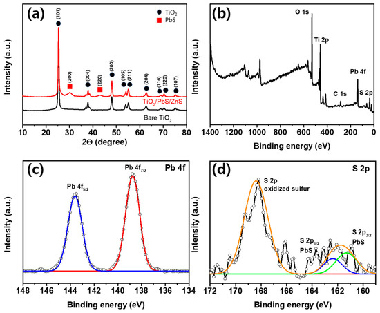
Figure 3.
(a) XRD spectra of bare TiO2 and TiO2/PbS/ZnS films. (b–d) XPS spectra of TiO2/PbS film. Survey scan (b) and high-resolution scans of Pb 4f (c) and S 2p region (d) (black lines with circle: measured spectrum, colored lines: fitted curves).
Figure 3b–d present the results of the XPS analysis conducted to verify the chemical states of the TiO2/PbS QD film. As seen in the survey scan of Figure 3b, Ti, O, Pb, S, and C are identified in the TiO2/PbS QD film. Figure 3c,d represents the high-resolution Pb 4f and S 2p spectra, respectively. The Pb 4f peaks exhibit binding energies (BEs) of 138.8 eV (Pb 4f7/2) and 143.6 eV (Pb 4f5/2), consistent with values for Pb-S bonds [41]. Additionally, the S 2p peaks have BEs of 161.2 eV (S 2p3/2) and 162.3 eV (S 2p1/2), also corresponding to values for Pb-S bonds [42]. The additional peaks at higher BEs at 166–171 eV exhibit the presence of oxidized sulfur groups, such as SO42− [43] or SO32− [44], indicating the partial oxidation of the PbS QD surface. This observed outcome is presumed to be a result of the SILAR process conducted in ambient air, which aligns with findings reported in previous studies [45].
Figure 4a,b shows the transmittance spectra and absorption spectra measured using UV-vis spectroscopy to evaluate the optical properties of the TiO2/PbS/ZnS films depending on the thicknesses. As shown in Figure 4a, the light transmittance gradually decreases with the increasing thickness of the transparent layer. Conversely, the absorbance of the film increases progressively in the wavelength range of 400 nm to 1100 nm as the thickness of the transparent layer becomes thicker, as shown in Figure 4b. These results arose from the absorption of incident light by the PbS QDs, and as the thickness of the TiO2/PbS/ZnS film increased, the loading of PbS QD was also enhanced, leading to a proportional increase in the absorbance. The improvement in absorbance across the entire visible and near-infrared (IR) spectrum is attributed to the narrow band-gap of PbS QDs. According to the previous literature [46], PbS exhibits an optical band-gap of approximately 0.41 eV in its bulk state; however, in the form of QDs with a size of approximately 4.8 nm, it demonstrates an optical band-gap of around 1.00 eV due to the quantum confinement effect. Given that the PbS QDs synthesized through the SILAR method in this study have a size of approximately 4.71 nm, it can be inferred that these QDs possess an optical band-gap slightly larger than 1.00 eV, absorbing photons of up to around 1200 nm wavelengths. This result indicates that as the film thickness increases, the loading of PbS QDs is enhanced, consequently improving the light absorption capability of the TiO2/PbS/ZnS film across the entire visible and near-IR spectrum.
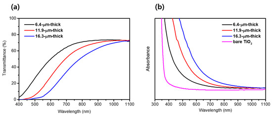
Figure 4.
(a) Transmittance spectra of TiO2 /PbS /ZnS films. (b) Absorbance spectra of bare TiO2 and TiO2/PbS/ZnS films.
Figure 5a shows the J–V characteristics of the TiO2/PbS/ZnS photoanodes depending on the thickness. The performance of each photoelectrode was measured under a 1-sun (100 mW/cm2) condition using a three-electrode system within a quartz reactor. The 11.9 µm thick photoanode exhibited the highest photocurrent density, with a value of 15.19 mA/cm2 at 0.6 VRHE. The other photoanodes showed photocurrent density values of 10.80 mA/cm2 (6.4 µm thick) and 11.93 mA/cm2 (16.3 µm thick), respectively, under the same condition. Compared to the 6.4 µm thick and 16.3 µm thick photoanodes, the photocurrent density was enhanced by 40.6% and 27.3%, respectively, for the optimized condition (11.9 µm thick), meaning that the photocatalytic activity of QD-decorated TiO2 for the sulfite oxidation was greatly affected by the film thickness. The obtained photocurrent density of 15.19 mA/cm2 from this study indicates a promising outcome for QD-decorated photoelectrodes when compared to previous reports as listed in Table S1 [22,47,48,49,50,51,52,53].
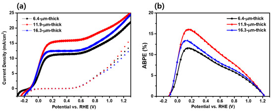
Figure 5.
(a) J–V curves and (b) ABPE curves of TiO2 /PbS /ZnS photoanodes according to the thickness.
Figure 5b shows the applied bias photon-to-current efficiency (ABPE) curves calculated using the following Equation (2) [54,55]:
where Jph represents the measured current density, Vapp is the applied external potential versus RHE and Pin is the power density of the incident light. The ABPE results aligned with the observed patterns in photocurrent density. Specifically, the 11.9 µm thick photoanode displayed the highest ABPE, reaching 16.17% at 0.153 V. In comparison, the 6.4 µm thick photoanode exhibited an ABPE of 11.70% at 0.143 V, while the 16.3 µm thick photoanode demonstrated an ABPE of 13.43% at 0.109 V.
To assess photostability, chronoamperometry was conducted at 0.6 VRHE for one hour, as shown in Figure 6a. The reduction in photocurrent density were observed as follows: 20.45% for the 6.4 µm thick photoanode, and 11.19% and 11.85% for the 11.9 µm thick and the 16.3 µm thick photoanode, respectively. As discussed above, as the thickness of the photoanode increases, the loading of PbS QDs is improved, leading to the enhanced absorbance and PEC performance of a photoanode. However, beyond a certain threshold, it is speculated that unfavorable factors such as increased electron recombination might lead to decreased performance [19,20]. Regardless of the thickness, it was observed that the photocurrent density decreased after 1 h in all three types of photoelectrodes. This is believed to be due to the decreased stability resulting from the facile oxidation of metal chalcogenides when used as electrodes in PEC hydrogen production [56,57]. This insufficient stability observed under illumination can be improved by applying effective overlayers for the passivation [10,58].
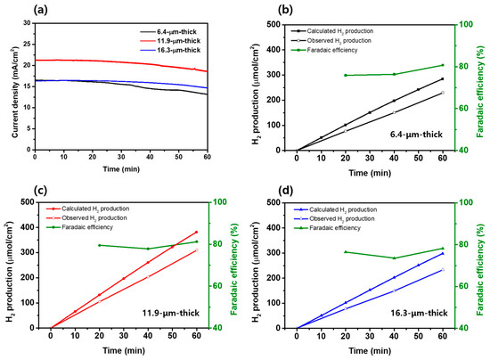
Figure 6.
(a) Chronoamperometric curves (at 0.6 VRHE) of TiO2/PbS/ZnS photoanodes. (b–d) Hydrogen production over time measured at 0.6 VRHE for 1 h, calculated theoretical hydrogen yield, and calculated faradaic efficiency for TiO2/PbS/ZnS photoanodes according to the thickness.
As represented in Figure 6b–d, the theoretical hydrogen generation was evaluated based on the chronoamperometry curves in Figure 6a, from Equation (3) [59]:
where F represents the Faraday constant, I is the measured photocurrent, and t is the measured time. The theoretically calculated hydrogen productions for each photoanode over the one hour are as follows: 284 µmol/cm2 (6.4 µm thick; Figure 6b), 382 µmol/cm2 (11.9 µm thick; Figure 6c), and 298 µmol/cm2 (16.3 µm thick; Figure 6d). Compared to the 6.4 µm thick and 16.3 µm thick photoanode, the hydrogen production was enhanced by 34.5%, 28.2%, respectively, for the optimized thickness condition (11.9 µm thick). The actual hydrogen production was measured at 0.6 VRHE for 1 h, as shown in Figure 6b–d. For each photoanode, the faradaic efficiency was retained between 73~81%. The 6.4 μm thick photoanode produced 230 μmol/cm2 over a period of 1 h (Figure 6b), the 11.9 μm thick photoanode produced 310 μmol/cm2 (Figure 6c), and the 16.3 μm thick photoanode produced 233 μmol/cm2 (Figure 6d), respectively. These results are matched well with the J–V curves for each photoanode, and indicate that the optimization of the photoanode thickness not only maximized the photocatalytic activity for the sulfite oxidation but also led to the actual maximum hydrogen production.
In addition, to thoroughly examine the influence of photoanode thickness on the charge transfer property, we conducted impedance analysis, as shown in Figure 7. The impedance spectra were obtained under the 1-sun condition (100 mW/cm2) at 0.6 VRHE, with a frequency range from 0.1 Hz to 100 kHz, and a sinusoidal perturbation of 10 mV. Using the equivalent circuit shown in Figure 7, we performed fitting in the Z-view program. The employed equivalent circuit consists of RS (solution resistance), Rct (charge transfer resistance), and CPE1 (constant phase element). The CPE represents the interfacial capacitance, which generally replaces a capacitor in the equivalent circuit for electrodes with high roughness [42]. The CPE parameter includes two parts: CPE-T, which represents the value of the capacitance, and CPE-P, known as the magnitude of the compression from an ideal semicircle in the Nyquist plot [60]. The Rct and CPE1 are related to the charge transfer characteristics at the interface of photoanode/redox electrolyte [10,61]. The values of each parameter corresponding to the thickness of the photoanode are listed in Table 1, and the value of the CPE parameters are listed in Table S2. The RS values were similar among the three photoanodes; however, the Rct value significantly decreased for the 11.9 µm thick photoanode. Compared to the 6.4 µm thick and 16.3 µm thick photoanode, it decreased by 37.1% and 30.0%, respectively, for the 11.9 µm thick photoanode, meaning that the charge transfer process occurs most efficiently for the 11.9 µm thick condition. This result is attributed to the improved light absorption capability compared to the 6.4 µm thick photoanode, and more favorable mass transfer of the electrolyte compared to the 16.3 µm thick photoanode.
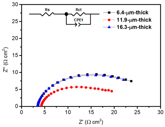
Figure 7.
Electrochemical impedance spectra of TiO2 /PbS /ZnS photoanodes according to the thickness under the 1-sun condition (100 mW/cm2) at 0.6 VRHE. The inset represents the equivalent circuit used for the fitting of impedance spectra.

Table 1.
Summary of J–V characteristics and electrochemical impedance parameters for TiO2/PbS/ZnS photoanodes according to the thickness.
4. Conclusions
In summary, our research underscores the pivotal role of optimizing the structure of PbS QD-decorated mesoporous TiO2 photoanodes to enhance the PEC hydrogen production performances. Through systematic investigation, we observed a clear correlation between the thickness of the photoanodes and their performance. Increasing the thickness of the photoanodes, within certain limits, resulted in enhanced light absorption capabilities across the visible and near-infrared spectrum. However, our findings demonstrate that the 11.9 µm thick photoanode yielded the most favorable balance, exhibiting an optimal photocurrent density of 15.19 mA/cm2, compared to the 6.4 µm thick and 16.3 µm thick counterparts. This optimal performance was attributed to the trade-off between its increased light absorption capacity and efficient electrolyte mass transfer, which was confirmed using the electrochemical impedance analysis by revealing the lowest charge transfer resistance in the 11.9 µm thick photoanode. The insights gained from this study will pave the way for the development of high-performance PEC hydrogen production devices.
Supplementary Materials
The following supporting information can be downloaded at: https://www.mdpi.com/article/10.3390/ma17010225/s1, Figure S1: (a) HR-TEM image and (b) lattice fringe of bare TiO2 nanoparticles; Figure S2: HR-TEM images of PbS QDs on the surface of TiO2 nanoparticles with lattice fringe; Figure S3: (a–c) Cross-sectional SEM images of bare TiO2 films according to the thickness; Table S1: Previously reported performances of QD-decorated photoelectrodes prepared by SILAR process for PEC hydrogen production; Table S2: Summary of fitting results of CPE parameters from EIS.
Author Contributions
Conceptualization, J.-Y.K.; methodology, Y.K., J.-W.S. and I.-H.L.; validation, J.-Y.K.; formal analysis, Y.K., J.-W.S. and I.-H.L.; investigation, Y.K., J.-W.S. and I.-H.L.; resources, J.-Y.K.; data curation, Y.K., J.-W.S. and I.-H.L.; writing—original draft preparation Y.K., J.-W.S. and I.-H.L.; writing—review and editing, J.-Y.K.; visualization, Y.K., J.-W.S. and I.-H.L.; supervision, J.-Y.K.; project administration, J.-Y.K.; funding acquisition, J.-Y.K. All authors have read and agreed to the published version of the manuscript.
Funding
This work was supported by the National Research Foundation of Korea (NRF) grant funded by the Korean government (MSIT) (grant no. 2020R1C1C1012014, 2021K2A9A1A06096526). This work was also supported by the Technology Innovation Program—Material Parts Technology Development Project (20017407, Development of Composite Filming Technology by Connection/Laminating with High Moisture, High Heat Resistance Transparent Film Resins and QD Distributed Layers with Large Area) funded by the Ministry of Trade, Industry & Energy (MOTIE, Korea). The following are also results of a study on the “Leaders in INdustry-university Cooperation 3.0” Project, supported by the Ministry of Education and National Research Foundation of Korea.
Institutional Review Board Statement
Not applicable.
Informed Consent Statement
Not applicable.
Data Availability Statement
All data are contained within the article.
Conflicts of Interest
The authors declare no conflicts of interest.
References
- Jin, L.; Zhao, H.; Wang, Z.M.; Rosei, F. Quantum Dots-based Photoelectrochemical Hydrogen Evolution from Water Splitting. Adv. Energy Mater. 2021, 11, 2003233. [Google Scholar] [CrossRef]
- Luo, B.; Liu, J.; Guo, H.; Liu, X.; Song, R.; Shen, K.; Wang, Z.M.; Jing, D.; Selopal, G.S.; Rosei, F. High Efficiency Photoelectrochemical Hydrogen Generation Using Eco-Friendly Cu Doped Zn-In-Se Colloidal Quantum Dots. Nano Energy 2021, 88, 106220. [Google Scholar] [CrossRef]
- Li, Z.; Channa, A.I.; Wang, Z.M.; Tong, X. Tailoring Eco-friendly Colloidal Quantum Dots for Photoelectrochemical Hydrogen Generation. Small 2023, 19, e2305146. [Google Scholar] [CrossRef]
- Cao, Q.; Yu, J.; Cao, Y.; Delaunay, J.-J.; Che, R. Unusual Effects of Vacuum Annealing on Large-Area Ag3PO4 Microcrystalline Film Photoanode Boosting Cocatalyst- and Scavenger-Free Water Splitting. J. Mater. 2021, 7, 929–939. [Google Scholar] [CrossRef]
- Yu, J.M.; Lee, J.; Kim, Y.S.; Song, J.; Oh, J.; Lee, S.M.; Jeong, M.; Kim, Y.; Kwak, J.H.; Cho, S.; et al. High-Performance and Stable Photoelectrochemical Water Splitting Cell with Organic-Photoactive-Layer-Based Photoanode. Nat. Commun. 2020, 11, 5509. [Google Scholar] [CrossRef]
- Kim, S.H.; Man, M.T.; Lee, J.W.; Park, K.-D.; Lee, H.S. Influence of Size and Shape Anisotropy on Optical Properties of CdSe Quantum Dots. Nanomaterials 2020, 10, 1589. [Google Scholar] [CrossRef]
- Ikram, A.; Dass, S.; Shrivastav, R.; Satsangi, V.R. Integrating PbS Quantum Dots with Hematite for Efficient Photoelectrochemical Hydrogen Production. Phys. Status Solidi A 2019, 216, 1800839. [Google Scholar] [CrossRef]
- Cao, Q.; Cheng, Y.-F.; Bi, H.; Zhao, X.; Yuan, K.; Liu, Q.; Li, Q.; Wang, M.; Che, R. Crystal Defect-Mediated Band-Gap Engineering: A New Strategy for Tuning the Optical Properties of Ag2Se Quantum Dots toward Enhanced Hydrogen Evolution Performance. J. Mater. Chem. A Mater. Energy Sustain. 2015, 3, 20051–20055. [Google Scholar] [CrossRef]
- Chen, H.; Pina, J.M.; Hou, Y.; Sargent, E.H. Synthesis, Applications, and Prospects of Quantum-dot-in-perovskite Solids. Adv. Energy Mater. 2022, 12, 2100774. [Google Scholar] [CrossRef]
- Kim, J.; Jang, Y.J.; Baek, W.; Lee, A.R.; Kim, J.-Y.; Hyeon, T.; Lee, J.S. Highly Efficient Photoelectrochemical Hydrogen Production Using Nontoxic CuIn1.5Se3 Quantum Dots with ZnS/SiO2 Double Overlayers. ACS Appl. Mater. Interfaces 2022, 14, 603–610. [Google Scholar] [CrossRef]
- Martinez, M.S.; Nozik, A.J.; Beard, M.C. Theoretical Limits of Multiple Exciton Generation and Singlet Fission Tandem Devices for Solar Water Splitting. J. Chem. Phys. 2019, 151, 114111. [Google Scholar] [CrossRef] [PubMed]
- Xing, Y.; Chen, X.; Jin, B.; Chen, P.; Huang, C.; Jin, Z. Photoelectrochemical Aptasensors Constructed with Photosensitive PbS Quantum Dots/TiO2 Nanoparticles for Detec-tion of Kanamycin. Langmuir 2021, 37, 3612–3619. [Google Scholar] [CrossRef] [PubMed]
- Mamiyev, Z.; Balayeva, N.O. PbS Nanostructures: A Review of Recent Advances. Mater. Today Sustain. 2023, 21, 100305. [Google Scholar] [CrossRef]
- Qian, Y.; Feng, J.; Wang, H.; Fan, D.; Jiang, N.; Wei, Q.; Ju, H. Sandwich-Type Signal-off Photoelectrochemical Immunosensor Based on Dual Suppression Effect of PbS Quantum Dots/Co3O4 Polyhedron as Signal Amplification for Procalcitonin Detection. Sens. Actuators B Chem. 2019, 300, 127001. [Google Scholar] [CrossRef]
- Seo, J.-W.; Ha, S.-B.; Song, I.-C.; Kim, J.-Y. PbS Quantum Dots-Decorated BiVO4 Photoanodes for Highly Efficient Photoelectrochemical Hydrogen Production. Nanomaterials 2023, 13, 799. [Google Scholar] [CrossRef]
- Li, L.; Dai, H.; Feng, L.; Luo, D.; Wang, S.; Sun, X. Enhance Photoelectrochemical Hydrogen-Generation Activity and Stability of TiO2 Nanorod Arrays Sensitized by PbS and CdS Quantum Dots under UV-Visible Light. Nanoscale Res. Lett. 2015, 10, 418. [Google Scholar] [CrossRef]
- Liu, R.; Fang, S.-Y.; Dong, C.-D.; Tsai, K.-C.; Yang, W.-D. Enhancing Hydrogen Evolution of Water Splitting under Solar Spectra Using Au/TiO2 Heterojunction Photo-catalysts. Int. J. Hydrogen Energy 2021, 46, 28462–28473. [Google Scholar] [CrossRef]
- Zheng, X.; Das, S.; Gu, Y.; Liu, S.; Zhao, J. Optimal Engineering of CdS/PbS Co-Sensitized TiO2 Nanotube Arrays for Enhanced Photoelectrochemical Performance. Ceram. Int. 2020, 46, 12050–12058. [Google Scholar] [CrossRef]
- Shin, I.; Seo, H.; Son, M.-K.; Kim, J.-K.; Prabakar, K.; Kim, H.-J. Analysis of TiO2 Thickness Effect on Characteristic of a Dye-Sensitized Solar Cell by Using Electrochemi-cal Impedance Spectroscopy. Curr. Appl. Phys. 2010, 10, S422–S424. [Google Scholar] [CrossRef]
- Ghicov, A.; Albu, S.P.; Hahn, R.; Kim, D.; Stergiopoulos, T.; Kunze, J.; Schiller, C.-A.; Falaras, P.; Schmuki, P. TiO2 Nanotubes in Dye-sensitized Solar Cells: Critical Fac-tors for the Conversion Efficiency. Chem. Asian J. 2009, 4, 520–525. [Google Scholar] [CrossRef]
- Zhang, S.; Yu, T.; Liu, Y.; Feng, M.; Li, X.; Sun, W.; Wang, D. A New SiP QDs/TiO2 NRs Composite Catalyst with Al2O3 Passivation Layer for Enhanced Photoelectro-chemical Water Splitting. Chem. Eng. J. 2022, 429, 132248. [Google Scholar] [CrossRef]
- Kim, J.-Y.; Jang, Y.J.; Park, J.; Kim, J.; Kang, J.S.; Chung, D.Y.; Sung, Y.-E.; Lee, C.; Lee, J.S.; Ko, M.J. Highly Loaded PbS/Mn-Doped CdS Quantum Dots for Dual Application in Solar-to-Electrical and Solar-to-Chemical Energy Conversion. Appl. Catal. B 2018, 227, 409–417. [Google Scholar] [CrossRef]
- Prasad, M.B.R.; Tamboli, P.S.; Ingle, R.V.; Diwate, K.D.; Baviskar, P.K.; Sankapal, B.R.; Mohite, K.C.; Jadkar, S.R.; Pathan, H.M. Geometrical thickness of titania pho-toanode as an influential parameter in controlling the photovoltaic performance of CdS quantum dot sensitized solar cells. Curr. Appl. Phys. 2017, 17, 1691–1698. [Google Scholar] [CrossRef]
- Altowyan, A.S.; Shaban, M.; Abdelkarem, K.; El Sayed, A.M. The Influence of Electrode Thickness on the Structure and Water Splitting Performance of Iridium Oxide Nanostructured Films. Nanomaterials 2022, 12, 3272. [Google Scholar] [CrossRef] [PubMed]
- Hernández, S.; Saracco, G.; Barbero, G.; Alexe-Ionescu, A.L. Role of the Electrode Morphology on the Optimal Thickness of BiVO4 Anodes for Photoelectrochemical Water Splitting Cells. J. Electroanal. Chem. 2017, 799, 481–486. [Google Scholar] [CrossRef]
- Sun, L.; Koh, Z.Y.; Wang, Q. PbS Quantum Dots Embedded in a ZnS Dielectric Matrix for Bulk Heterojunction Solar Cell Applications. Adv. Mater. 2013, 45, 4598–4604. [Google Scholar] [CrossRef]
- Xie, C.; Yang, S.; Shi, J.; Niu, C. Highly Crystallized C-Doped Mesoporous Anatase TiO2 with Visible Light Photocatalytic Activity. Catalysts 2016, 6, 117. [Google Scholar] [CrossRef]
- Gnanasekaran, L.; Hemamalini, R.; Ravichandran, K. Synthesis and Characterization of TiO2 Quantum Dots for Photocatalytic Application. J. Saudi Chem. Soc. 2015, 19, 589–594. [Google Scholar] [CrossRef]
- Shen, F.; Que, W.; Liao, Y.; Yin, X. Photocatalytic Activity of TiO2 Nanoparticles Sensitized by CuInS2 Quantum Dots. Ind. Eng. Chem. Res. 2011, 50, 9131–9137. [Google Scholar] [CrossRef]
- Kaur, A.; Umar, A.; Kansal, S.K. Sunlight-Driven Photocatalytic Degradation of Non-Steroidal Anti-Inflammatory Drug Based on TiO2 Quantum Dots. J. Colloid. Interface Sci. 2015, 459, 257–263. [Google Scholar] [CrossRef]
- Shafaee, M.; Goharshadi, E.K.; Mashreghi, M.; Sadeghinia, M. TiO2 Nanoparticles and TiO2 @graphene Quantum Dots Nancomposites as Effective Visible/Solar Light Photocatalysts. J. Photochem. Photobiol. A Chem. 2018, 357, 90–102. [Google Scholar] [CrossRef]
- Sharma, S.; Umar, A.; Mehta, S.K.; Ibhadon, A.O.; Kansal, S.K. Solar Light Driven Photocatalytic Degradation of Levofloxacin Using TiO2/Carbon-Dot Nanocomposites. New J. Chem. 2018, 42, 7445–7456. [Google Scholar] [CrossRef]
- Sood, S.; Mehta, S.K.; Umar, A.; Kansal, S.K. The Visible Light-Driven Photocatalytic Degradation of Alizarin Red S Using Bi-Doped TiO2 Nanoparticles. New J. Chem. 2014, 38, 3127–3136. [Google Scholar] [CrossRef]
- Kanniainen, T.; Lindroos, S.; Ihanus, J.; Leskelä, M. Growth of Strongly Orientated Lead Sulfide Thin Films by Successive Ionic Layer Adsorption and Reaction (SILAR) Technique. J. Mater. Chem. 1996, 6, 161–164. [Google Scholar] [CrossRef]
- El-Menyawy, E.M.; Mahmoud, G.M.; Ibrahim, R.S.; Terra, F.S.; El-Zahed, H.; El Zawawi, I.K. Structural, Optical and Electrical Properties of PbS and PbSe Quantum Dot Thin Films. J. Mater. Sci. Mater. Electron. 2016, 27, 10070–10077. [Google Scholar] [CrossRef]
- Emeakaroha, T.M. Optical and Structural Properties of Silar-Grown Highly Oriented Lead Sulphide (PbS) Thin Films. Chalcogenide Lett. 2016, 13, 91–96. [Google Scholar]
- Yu, Y.; Zhang, K.; Sun, S. One-Pot Aqueous Synthesis of near Infrared Emitting PbS Quantum Dots. Appl. Surf. Sci. 2012, 258, 7181–7187. [Google Scholar] [CrossRef]
- He, X.; Demchenko, I.N.; Stolte, W.C.; van Buuren, A.; Liang, H. Synthesis and Transformation of Zn-Doped PbS Quantum Dots. J. Phys. Chem. C Nanomater. Interfaces 2012, 116, 22001–22008. [Google Scholar] [CrossRef]
- Cullity, B.D. Elements of X-ray Diffraction, 2nd ed.; Addison-Wesley Pub. Co.: Reading, MA, USA, 1978. [Google Scholar]
- Wichaiyo, N.; Kitiwan, M.; Shen, Q.; Yindeesuk, W. The Effect of PbS Colloidal Quantum Dots with CdS and ZnS Coating on Photovoltaic Properties. Curr. Appl. Sci. Technol. 2022, 23, 14. [Google Scholar] [CrossRef]
- Jiang, P.; Liu, Z.-F.; Cai, S.-M. Growing Monodispersed PbS Nanoparticles on Self-Assembled Monolayers of 11-Mercaptoundecanoic Acid on Au(111) Sub-strate. Langmuir 2002, 18, 4495–4499. [Google Scholar] [CrossRef]
- Hardman, S.J.O.; Graham, D.M.; Stubbs, S.K.; Spencer, B.F.; Seddon, E.A.; Fung, H.-T.; Gardonio, S.; Sirotti, F.; Silly, M.G.; Akhtar, J.; et al. Electronic and Surface Prop-er-ties of PbS Nanoparticles Exhibiting Efficient Multiple Exciton Generation. Phys. Chem. Chem. Phys. 2011, 13, 20275. [Google Scholar] [CrossRef] [PubMed]
- Jiang, X.-X.; Xue, J.-Y.; Zhao, Z.-Y.; Li, C.; Li, F.-L.; Cao, C.; Niu, Z.; Gu, H.-W.; Lang, J.-P. Ultrathin Sulfate-Intercalated NiFe-Layered Double Hydroxide Nanosheets for Efficient Electrocatalytic Oxygen Evolution. RSC Adv. 2020, 10, 12145–12150. [Google Scholar] [CrossRef] [PubMed]
- Pieczyńska, A.; Mazierski, P.; Lisowski, W.; Klimczuk, T.; Zaleska-Medynska, A.; Siedlecka, E. Effect of Synthesis Method Parameters on Properties and Photoelectrocatalytic Activity under Solar Irradiation of TiO2 Nanotubes Decorated with CdS Quantum Dots. J. Environ. Chem. Eng. 2021, 9, 104816. [Google Scholar] [CrossRef]
- Sung, S.D.; Lim, I.; Kang, P.; Lee, C.; Lee, W.I. Design and development of highly efficient PbS quantum dot-sensitized solar cells working in an aqueous polysulfide elec-trolyte. Chem. Commun. 2013, 49, 6054. [Google Scholar] [CrossRef] [PubMed]
- Hyun, B.-R.; Zhong, Y.-W.; Bartnik, A.C.; Sun, L.; Abruna, H.D.; Wise, F.W.; Goodreau, J.D.; Matthews, J.R.; Leslie, T.M.; Borrelli, N.F. Electron injection from colloidal PbS quantum dots into titanium dioxide nanoparticles. ACS Nano 2008, 2, 2206–2212. [Google Scholar] [CrossRef] [PubMed]
- Choi, Y.; Yim, C.; Baek, S.; Choi, M.; Jeon, S.; Yong, K. In Situ Measurement of Photostability of CdSe/CdS/ZnO Nanowires Photoelectrode for Photoelectrochemical Water Splitting. Sens. Actuators B Chem. 2015, 221, 113–119. [Google Scholar] [CrossRef]
- Freitas, D.V.; González-Moya, J.R.; Soares, T.A.S.; Silva, R.R.; Oliveira, D.M.; Mansur, H.S.; Machado, G.; Navarro, M. Enhanced Visible-Light Photoelectrochemical Conversion on TiO2 Nanotubes with Bi2S3 Quantum Dots Obtained by in Situ Electrochemical Method. ACS Appl. Energy Mater. 2018, 1, 3636–3645. [Google Scholar] [CrossRef]
- Chen, S.; Li, C.; Hou, Z. A Novel in Situ Synthesis of TiO2/CdS Heterojunction for Improving Photoelectrochemical Water Splitting. Int. J. Hydrogen Energy 2019, 44, 25473–25485. [Google Scholar] [CrossRef]
- Mezzetti, A.; Balandeh, M.; Luo, J.; Bellani, S.; Tacca, A.; Divitini, G.; Cheng, C.; Ducati, C.; Meda, L.; Fan, H.; et al. Hyperbranched TiO2–CdS Nano-Heterostructures for Highly Efficient Photoelectrochemical Photoanodes. Nanotechnology 2018, 29, 335404. [Google Scholar] [CrossRef]
- Zhang, H.; Zhang, D.; Qin, X.; Cheng, C. Three-Dimensional CdS-Sensitized Sea Urchin like TiO2-Ordered Arrays as Efficient Photoelectrochemical Anodes. J. Phys. Chem. C Nanomater. Interfaces 2015, 119, 27875–27881. [Google Scholar] [CrossRef]
- Zhang, Z.; Li, X.; Gao, C.; Teng, F.; Wang, Y.; Chen, L.; Han, W.; Zhang, Z.; Xie, E. Synthesis of Cadmium Sulfide Quantum Dot-Decorated Barium Stannate Nanowires for Photoelectrochemical Water Splitting. J. Mater. Chem. A Mater. Energy Sustain. 2015, 3, 12769–12776. [Google Scholar] [CrossRef]
- Ma, D.; Shi, J.-W.; Zou, Y.; Fan, Z.; Ji, X.; Niu, C. Highly Efficient Photocatalyst Based on a CdS Quantum Dots/ZnO Nanosheets 0D/2D Heterojunction for Hydrogen Evolution from Water Splitting. ACS Appl. Mater. Interfaces 2017, 9, 25377–25386. [Google Scholar] [CrossRef]
- Li, S.; Jung, S.-M.; Chung, W.; Seo, J.-W.; Kim, H.; Park, S.I.; Lee, H.C.; Han, J.S.; Ha, S.B.; Kim, I.Y.; et al. Defect Engineering of Ternary Cu–In–Se Quantum Dots for Boosting Photoelectrochemical Hydrogen Generation. Carbon. Energy 2023, 5, e384. [Google Scholar] [CrossRef]
- Liu, C.; Qiu, Y.; Wang, F.; Wang, K.; Liang, Q.; Chen, Z. Design of Core-Shell-structured ZnO/ZnS Hybridized with Graphite-like C3N4 for Highly Efficient Photoe-lec-trochemical Water Splitting. Adv. Mater. Interfaces 2017, 4, 1700681. [Google Scholar] [CrossRef]
- Mo, Q.-L.; Hou, S.; Wei, Z.-Q.; Fu, X.-Y.; Xiao, G.; Xiao, F.-X. Fine Tuning of Charge Motion over Homogeneous Transient Metal Chalcogenides Heterostructured Photoanodes for Photoelectrochemical Water Splitting. Chem. Eng. J. 2022, 433, 133641. [Google Scholar] [CrossRef]
- Cho, S.; Jang, J.-W.; Lee, K.-H.; Lee, J.S. Research Update: Strategies for Efficient Photoelectrochemical Water Splitting Using Metal Oxide Photoanodes. APL Mater. 2014, 2, 010703. [Google Scholar] [CrossRef]
- Li, H.; Wen, P.; Hoxie, A.; Dun, C.; Adhikari, S.; Li, Q.; Lu, C.; Itanze, D.S.; Jiang, L.; Carroll, D.; et al. Interface Engineering of Colloidal CdSe Quantum Dot Thin Films as Acid-Stable Photocathodes for Solar-Driven Hydrogen Evolution. ACS Appl. Mater. Interfaces 2018, 10, 17129–17139. [Google Scholar] [CrossRef]
- Alvi, N.H.; Soto Rodriguez, P.E.D.; Aseev, P.; Gómez, V.J.; Alvi, A.H.; Hassan, W.; Willander, M.; Nötzel, R. InN/InGaN Quantum Dot Photoelectrode: Efficient Hydrogen Generation by Water Splitting at Zero Voltage. Nano Energy 2015, 13, 291–297. [Google Scholar] [CrossRef]
- Kim, J.-Y.; Kim, J.Y.; Lee, D.-K.; Kim, B.; Kim, H.; Ko, M.J. Importance of 4-Tert-Butylpyridine in Electrolyte for Dye-Sensitized Solar Cells Employing SnO2 Electrode. J. Phys. Chem. C 2012, 116, 22759–22766. [Google Scholar] [CrossRef]
- Li, F.; Zhang, M.; Benetti, D.; Shi, L.; Besteiro, L.V.; Zhang, H.; Liu, J.; Selopal, G.S.; Sun, S.; Wang, Z.; et al. “Green”, Gradient Multi-Shell CuInSe2/(CuInSexS1−x)5/CuInS2 Quantum Dots for Photo-Electrochemical Hydrogen Generation. Appl. Catal. B 2021, 280, 119402. [Google Scholar] [CrossRef]
Disclaimer/Publisher’s Note: The statements, opinions and data contained in all publications are solely those of the individual author(s) and contributor(s) and not of MDPI and/or the editor(s). MDPI and/or the editor(s) disclaim responsibility for any injury to people or property resulting from any ideas, methods, instructions or products referred to in the content. |
© 2023 by the authors. Licensee MDPI, Basel, Switzerland. This article is an open access article distributed under the terms and conditions of the Creative Commons Attribution (CC BY) license (https://creativecommons.org/licenses/by/4.0/).