Abstract
This study aims to determine the optimum composition of the CeBr1−xIx compound to achieve the maximum light output. It is based on calculations of the band energy structure of crystals, specifically taking into account the characteristics of the mutual location of local and band 5d states of the Ce3+ ions. The band energy structures for CeBr2I and CeBrI2 crystals were calculated using the projector augmented wave method. The valence band was found to be formed by the hybridized states of 4p Br and 5p I. The 4f states of Ce3+ are located in the energy forbidden band gap. The conduction band is formed by the localized 5d1 states, which are created by the interaction between the 5d states of Ce3+ and the 4f0 hole of the cerium ion. The higher-lying delocalized 5d2 states of Ce3+ correspond to the energy levels of the 5d states of Ce3+ in the field of the halide Cl0 (Br0) hole. The relative location of 5d1 and 5d2 bands determines the intensity of 5d–4f luminescence. The bottom of the conduction band is formed by localized 5d1 states in the CeBr2I crystal. The local character of the bottom of the conduction band in the CeBr2I crystal favors the formation of self-trapped Frenkel excitons. Transitions between the 5d1 and 4f states are responsible for 5d–4f exciton luminescence. In the CeBrI2 crystal, the conduction band is formed by mixing the localized 5d1 and delocalized 5d2 states, which leads to quenching the 5d–4f luminescence and a decrease in the light output despite the decrease in the forbidden band gap. CsBr2I is the optimum composition of the system to achieve the maximum light output.
1. Introduction
Nowadays, there is a need for the mass production of reliable, highly sensitive, and cheap sensors for radiation monitoring of the environment [1], global tracking of radioactive materials [2,3], medicine [4], energy sector, Internet of Things [5,6], etc. There are known metrological methods for improving the accuracy of sensors such as calibration and diagnostics [7], technical methods such as designing new constructions [5], and mathematical methods such as data processing techniques [7]. However, these methods do not eliminate the reasons of sensor inaccuracies. Thus, deep fundamental studies are essential to develop robust sensors.
The main requirements for scintillation materials concern such scintillator parameters as light output and speed. The need for high-speed characteristics has especially increased with the need to develop scintillators to fully use the possibilities of positron emission tomography operating in the time-of-flight registration mode [8], with respect to spatial separation in medical imaging.
Recently, among many potential scintillators, attention is focused on nanocrystals of halide perovskites, which exhibit short decay times (<15 ns) and high light yields [9]. However, the challenge of compacting nanocrystals into bulk transparent samples has led researchers to turn to single crystalline objects. Certain potential for time resolution lies in lanthanide halide crystals, particularly LaBr3–Ce, which shows a coincidence time resolution of 77 ps [10], which is almost comparable with 51 ps of BaF2 [11,12], demonstrating one of the shortest luminescence decay times (0.8 ns) among crystalline scintillators. Therefore, efforts aimed at improving the parameters of the existing fast scintillators, whose growth technology was developed [13], are welcomed.
The relevance of the study presented in this work is determined by the search for fast scintillators suitable for application as detectors in positron emission tomography systems in the time-of-flight mode. This study aims to determine the optimum composition of the CeBr3−xIx compound to achieve maximum light output. This is based on calculations of the band energy structure of crystals, in particular, considering the peculiarities of the mutual location of the local and band states of the Ce3+ ion.
Heavy inorganic crystals of cerium trihalide are thought to be promising scintillators for their use as radiation detectors in high-energy physics and medicine. The above-mentioned crystals gained popularity because of fast decay time constant and high light yield of 5d–4f Ce3+ transitions. The CeBr3 crystal is the most efficient among CeX3 (X = F, Cl, Br, I) crystals and has light yield (LY) > 60,000 photons/MeV and 4% energy resolution at 662 KeV [14]. The CeI3 crystal, which has a much smaller forbidden band gap (Eg), does not have such a high luminescence efficiency, as it is expected according to the fundamental light yield limit, which is inversely proportional to the value of Eg [15]:
where β is a constant, Eg is a forbidden band gap of the solid, S characterizes the efficiency of energy transfer from the electron–hole pairs to the scintillating ions, and QE is the quantum efficiency of luminescence.
In addition to the search for scintillation materials with low Eg, there is another approach to increase light yield related to the efficiency (S) of energy transfer to the luminescence center. This approach is based on the synthesis of mixed crystals [16]. The mixed crystals promote the formation of phonons with energy greater than that in original crystals, and new phonon branches for energy relaxation appear [17]. An increase in light yield was observed for (Lu,Y)AP:Ce mixed crystals with an intermediate concentration of Lu/Y [18] and for Gd3(Al,Ga)5O12 crystals (GAGG) with an Al/Ga ratio of 2/3 [19]. Mixed oxide scintillators LYSO demonstrate a 10–30% higher light output [20,21].
The authors of [22] also claim that, in crystals with the hybrid structure of halogens, the scintillation properties become better with the decrease in the hot electron thermalization length, which improves the S parameter. As the phonon energy increases, the length of electron thermalization decreases, which reduces the probability of electron capture at defects and increases the luminescence intensity. The additional phonon branches accelerate electron relaxation processes as well. In the mixed crystals, where the phonon subsystem plays an important role, it is necessary to consider the peculiarities of the structure of the electronic energy of crystals, which also affects the efficiency of luminescence processes. The reduction in the thermalization length through the cation disorder in rare-earth metal lithium halides leads to a decrease in or blocking of diffusion pathways [23]. Recent experimental studies showed that the luminescence properties of CeI3 and CeBr3 can be significantly improved by changing the concentration of substituted halogen x in the structure of CeBr3−xIx [24]. In particular, it was shown that Sr co-doping of CeBr3 improves its energy resolution [25], and the light output of other halide binary compositions increases upon mixing halides [16,26]. It was also demonstrated that the halide substitution of Eu in CsCaI3 crystals [27] as well as in CsSrBrI2, CsCaBrI2, and CsSrClBr2 crystals [28] enhances the luminescent properties of such materials by modifying their structure.
Scintillators based on lanthanide halides activated with cerium were patented as early as 2008 [13]. The next step in the development of lanthanide-based scintillators is the transition to self-activated scintillators based on cerium, CeX3, which, similar to LaX3–Ce, exhibit commensurable scintillation parameters but, due to their higher atomic number Z, demonstrate higher absorption capability for ionizing radiation. Additionally, they show lower background radiation compared with LaX3 [29].
The idea of enhancing the scintillation parameters of cerium halide scintillators, specifically CeBr3, through mixed halide crystals Ce(Br,I)3, is inspired by the demonstrated improvement in the timing properties of the La(Br,I)3:Ce system [30]. This concept is also supported by numerous studies showing a general trend of improving scintillation parameters in mixed halide single crystal scintillators. For instance, in the system with the general formula of CeBr3−xClx, where 0 ≤ x ≤ 3, the light yield changed from 44,000 to 60,000 photons/MeV under 137Cs γ-ray irradiation when transitioning from CeCl3 to CeBr3. Therefore, the attempts to improve the light output in the CeBr3−xIx system [24] are well founded. These attempts were motivated by certain features of the scintillation process that contribute to an increase in the light output. The decrease in the band gap was expected to enhance the light output by substituting bromine with iodine. Indeed, the transition from CeBr3 to CeBr2I increases the light output from 60,000 to 70,000 photons/MeV [24]. However, further increase in the iodine content resulted in a deterioration of the scintillation parameters. Based on our previous research on the energy structure of CeX3 crystals (X = F, Cl, Br, I) [31,32], we aim to demonstrate that the decrease in the light output is caused by peculiarities in the band energy structure of self-activated cerium halide crystals. The conduction band in these crystals is formed by the 5d states of Ce3+ ions. The 5d1 electrons of the Ce3+ ion in an electric field of a 4f0 hole form a conduction sub-band (5d1). It is responsible for the 5d–4f excitonic luminescence of cerium ions. The 5d electrons, in the presence of a halide hole (npX0), form a higher-lying band (5d2) with delocalized electrons. The overlap between the localized (5d1) and delocalized (5d2) states leads to significant quenching of the excitonic luminescence, which must be the cause of CeBrI2 luminescence quenching.
In the case of the mixed CeBr3−xIx crystal, there is only a certain range of x values at which success can be achieved because in CeBr3, the bottom of the conduction band is formed by local states that promote exciton 5d–4f luminescence, whereas in CeI3, the bottom of the conduction band is formed by delocalized states. As a result, 5d–4f luminescence in room temperature becomes negligible [31]. Therefore, for a better understanding of the physical processes that occur after this kind of substitution, this paper presents the results of theoretical studies of the energy structure for the CeBr2I and CeBrI2 crystals, as well as the influence of the location of localized and delocalized 5d states on the luminescence efficiency.
We intend to theoretically predict the optimum composition of the CeBr3−xIx mixture to achieve the highest light output. It is expected that reducing the forbidden band gap and appearing additional channels for electron thermalization through iodine substitution can improve the light output. We plan to demonstrate that, in addition to band-gap reduction, the energy structure of the CeBr3−xIx conduction band will also change, leading to a decrease in the light output. The localized 5d states of cerium ions, associated with the formation of Frenkel excitons, will overlap with the delocalized states of the conduction band, resulting in luminescence quenching. We aim to show that CeBr2I crystals are the optimum composition for achieving the maximum output in the CeBr3−xIx system. This is possible because CeI3 represents the case where delocalized and localized states strongly overlap, leading to luminescence quenching.
2. Modeling and Calculations
All calculations were performed within the framework of the density functional theory using Abinit v8.10 software [33] distributed under the open-source license. Lattice constants obtained using X-ray spectroscopy [24] were used as input data to calculate the main energy parameters of the CeBr2I and CeBrI2 crystals. Crystal cells (Figure 1) were modeled with Avogadro 1.91.0 software using constants and space symmetry groups shown in Table 1.
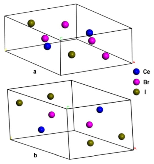
Figure 1.
Modeled cells of CeBr2I (a) and CeBrI2 (b) crystals.

Table 1.
Crystal lattice parameters and space groups for the CeBr2I and CeBrI2 crystals.
As can be seen from Table 1, the CeBr2I crystal has the hexagonal lattice similar to CeCl3, CeBr3, and CeF3. The CeBrI2 crystal has the orthorhombic lattice similar to CeI3. The symmetry of the lattice varies depending on the iodine concentration. According to the experimental data presented in [24], the structure of CeBr3−xIx changes to orthorhombic when x > 0.5.
The projector augmented wave (PAW) method was used [34] to provide accurate representation of energy properties with respect to the fast-oscillating components of the wave functions of electrons near the cores. This method combines features of both the pseudopotential approach and the plane wave method. The connection between the wave function and the pseudo-wave function can be expressed by the formula
where
- —atomic wave function,
- —pseudo-wave function,
- —projector function.
The sum is performed out of the spheres of joining, which are numbered with the index a. The index i = {n, l, m} corresponds to quantum numbers—the principal, orbital, and magnetic, respectively.
From (4), it is easy to see that
where transforms the pseudo-wave function into the electron wave function .
The explicit form of the operator is derived from (2):
The stationary Schrödinger equation is as follows:
which will become as follows when taking into account (3):
with the same desired electron spectrum as in (7).
The electron density in the PAW method is determined by three additions:
The first addition is a smooth pseudo-density , which can be described by the Fourier transform:
where
- —the occupation numbers of one-electron state,
- k—a vector of the first Brillouin zone,
- n—the number of filled electronic bands,
- —the volume of the primitive lattice,
- —is a vector of the reciprocal lattice of the crystal.
For the electronic function, Formula (8) is as follows:
There is a significant difference between Formulae (8) and (9). Equation (9) considers ~103 vectors G, but achieving the same level of accuracy for Equation (8) requires ~106 vectors. That is why it is impossible to solve Equation (7) using the electronic function even when embracing supercomputers.
The next two additions of electronic densities inside the augmented sphere are determined by the projected coefficients of filled states:
and
The idea of the PAW method is transforming the Schrödinger equation into the form where the unknown function of state is . It is much less computationally expensive than the original one . If the function is found, using the transformation operator , it is easy to obtain the state function . The Hartree potential and electron densities can be calculated using .
One of the features of the lanthanide ions is the presence of highly localized states with exchange-correlation energy that cannot be correctly described by either the local density approximation (LDA) model or its generalized gradient modification (GGA) [35]. The approximation of the above-mentioned exchange-correlation interaction functionals is based on the model of the homogeneous electron gas, which, however, contradicts the localization of the electron density in narrow energy regions for the lanthanide ions. Two approaches were considered to solve this problem: the use of the hybrid functional of the exchange-correlation interaction PBE0 [36] and Hubbard corrections in the DFT + U method [37]. The former works better for crystals with a high concentration of lanthanide ions where they are constitutional ions of the matrix [32]. On the other hand, the DFT + U method is accurate enough to describe the energy states of lanthanides when computational power is limited.
All calculations were performed on the Monkhorst–Pack grid with the size of 10 × 10 × 10. The basis of wave functions was formed by plane waves with cutoff energies of 48 Ha (1306.15 eV) and 108 Ha (2938.83 eV) within the PAW sphere. For an accurate representation of the conduction band, 200 energy states of the investigated crystals were considered in the calculations.
The well-known formula was used to calculate the effective mass of electrons:
For a free particle, the dispersion law is quadratic, so the effective mass is constant and equal to the mass of rest of the electron m0. The situation is more complicated in a crystal, and the dispersion law differs from the quadratic one. Nevertheless, the dispersion law E(k) curve near the extrema is usually well approximated by a parabola, where the effective mass is also a constant, although different from m0. At the same time, can be positive (near the bottom of the conduction band) and negative (near the top of the valence band). The tensor nature of the effective mass in anisotropic crystals illustrates that in the crystal lattice, an electron moves as a quasiparticle, and its movement is controlled by the direction relative to the crystallographic axes of the crystal. However, the value of is determined not by energy but by the state, which is based on vector k. In this work, the effective mass was obtained after post-processing of the calculated energy band structure. Abipy software 0.8.0 was used to analyze the raw output data of Abinit v8.10, which allows calculating various physical characteristics based on the information about the energy structure of the crystal using Python programming language. The developed software allowed us to estimate the value of the effective mass of charge carriers at any pre-calculated energy level in the proximity of a given k-point performing approximation by a paraboloid in a three-dimensional k-space. All presented values of in this paper were obtained around the highly symmetrical point Γ, in which, for these cases, the energy of the conduction band reaches its minimum.
3. Results and Discussions
The calculated partial and total densities of states of the CeBr2I and CeBrI2 crystals are presented in Figure 2 and Figure 3, respectively. The top of the valence band in both cases is formed by the hybridized states of 4p Br and 5p I. The valence bandwidth of the CeBr2I crystal is 4 eV, which is 1 eV larger than in the case of CeBrI2.
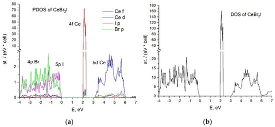
Figure 2.
CeBr2I crystal (a) partial density of states; (b) total density of states.
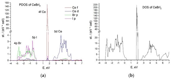
Figure 3.
CeBrI2 crystal (a) partial density of states; (b) total density of states.
There are 4f cerium states in the middle of the forbidden zone. Their peaks of 0.3 eV width are located above the valence band by 2 eV for CeBr2I and 1.6 eV for CeBrI2.
The conduction band is formed by 5d Ce states in both cases, demonstrating different distributions of the density of states. The contribution of 4p Br- and 5p I- states to the conduction band is negligible.
The energy band structures of the CeBr2I and CeBrI2 crystals are presented in Figure 4. The energy parameters of the bands were calculated along the high-symmetry paths of the Brillouin zone: Γ-K-L-A-H-Γ for CeBr2I and Γ-X-S-Y-Γ-Z for CeBrI2. The energy band structures of the CeBr3 and CeI3 crystals [31] are presented for comparison.
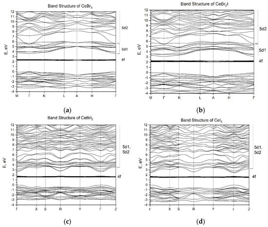
Figure 4.
The energy band structure of CeBr3−xIx crystal: (a) CeBr3, (b) CeBr2I, (c) CeBrI2, (d) CeI3.
The clear localization of 4f-states and the formation of localized (5d1) and delocalized (5d2) 5d-states of cerium ions in the conduction band, as shown for CeBr3 (see Figure 4a) [31], are features of the electronic structure of the self-activated CeX3 scintillators. Conclusions about the peculiarities of 5d-state localization in the conduction band were drawn based on the difference between the effective masses of electrons in the bottom of the conduction band and electrons in the depth of the conduction band. Additional evidence for the existence of the local 5d1 states of cerium ions in self-activated CeX3 is the presence of typical luminescence of the cerium 4f–5d ions. In the CeBr2I crystal, the energy sub-bands 5d1 and 5d2 with different effective masses of electrons ( (5d1) = 1.99 m0 and (5d2) = 0.58 m0) can also be distinguished. The width of the 5d1 sub-band at Γ-point is the splitting of the 5d states of cerium ions by the crystal field of the matrix. Excitation of electrons in the 5d2 sub-band does not necessarily lead to luminescence, as the high mobility of electrons leads to their significant diffusion, which negatively affects the efficiency of their recombination with holes [31,32]. The energy gap between the top of the halide valence band and the 5d2 sub-band of the conduction band is considered as the value of the forbidden band gap (Eg). The parameters of the energy bands of the CeBr3, CeBr2I, CeBrI2, and CeI3 crystals are given in Table 2. The table also shows the position of 4f-cerium levels relative to the top of the valence band (E4f) and the energy of 4f–5d transitions (E4f–5d). The energy of the forbidden band gap for CeBr3 (Eg = 5.7 eV) agrees well with the experimental data for the LaBr3 crystal (Eg = 5.9 eV), where the conduction band is formed by delocalized 5d-states. However, for the CeI3 crystal, the band gap (Eg = 2.4 eV) is underestimated in comparison with the experimental results (Eg = 3.8 eV) [31]. The results for the energy of 4f–5d transitions for all crystals are also underestimated. Since the experimental data for Eg in CeBr2I and CeBrI2 crystals are not available, the calculated results of Eg = 5.4 eV and Eg = 2.6 eV should be considered as approximate values. Such underestimation of the energy parameters is a well-known problem for DFT calculations [38]. Other theoretical approaches (such as the Green function method) can provide a more accurate value of the band gap, but the positions of 4f states will be less precise. However, the used method allowed us to determine the features of the structure of the conduction band such as the existence of localized and delocalized 5d states of cerium. The presence of localized states at the bottom of the conduction band allows us to apply the model of Frenkel self-trapped excitons to explain the 5d–4f luminescence of cerium ions. The increase in the overlap of localized and delocalized states with increasing iodine concentration explains the tendency of light yield decrease (CeBrI2, CeI3) due to the decrease in quantum efficiency (QE). The calculation method also shows a general trend of decrease in the band gap with the increase in iodine concentration, which explains the increase in the CeBr2I light yield compared with CeBr3.
With respect to the peculiarities of the conduction band of CeX3 crystals, the conduction band of the CeBrI2 crystal (Figure 4c) shows similar characteristics to CeI3 (Figure 4d). The dispersion of the bottom of the conduction band with respect to the wave vector k is higher in the case of CeBrI2 compared with CeBr2I and CeBr3. It is characterized by a small effective electron mass of 1.03 m0, which is typical for delocalized conduction band states. By analyzing the dependence of the forbidden energy band gap on the concentration of iodine ions, it can be noted that it decreases with the increase in iodine concentration in the following direction:
This series in a descending order of the band gap allows us to see the general trend of the influence of the substitution of the bromide ions with the iodine ones on the forbidden band gap of the crystal. Comparing the luminescence properties of the CeBr3, CeBr2I, CeBrI2, and CeI3 crystals according to the fundamental light yield limit (1), which is inversely proportional to the band gap, it is expected that the scintillation efficiency will increase in the order shown in (14). Indeed, as mentioned above, the transition from CeBr3 to CeBr2I leads to the increase in light yield from 40,000 to 70,000 photons/MeV, consistent with the dependence of light yield on Eg. In the case of the mixed CeBr2I crystal, light output increases not only due to a decrease in Eg but also due to an increase in the efficiency of energy transfer to the luminescent centers (S) because of the presence of additional phonon branches. This contributes to faster relaxation of electrons in the conduction band.
Further increase in the concentration of iodine leads to the decrease in the band gap width, which should increase the intensity of the luminescence light. However, in practice, the situation is opposite; for CeBrI2, LY is 50,000 photons/MeV, and for CeI3, it is 5000 photons/MeV. To explain this dependence, it is necessary to analyze the position of the local 5d1 state relatively to the delocalized 5d2 one. The schemes in Figure 5 show that in contrast to CeBr3 (Figure 4a) and CeBr2I (Figure 4b) crystals, the 5d1 and 5d2 states in CeBrI2 and CeI3 crystals overlap, and the bottom of the conduction band is formed by delocalized states with the effective mass of electrons of 1.03 m0 for CeBrI2 and 0.26 m0 for CeI3. Taking into account these small effective masses, the bottom of the conduction band will be formed by delocalized states. The 5d→4f luminescence from such states should be very weak or completely absent, demonstrating significant temperature dependence of the luminescence intensity. Therefore, for CeBrI2 and CeI3 crystals, the values of the light yield are determined by the low quantum efficiency (QE) of the luminescence process.
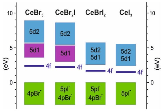
Figure 5.
Schemes of calculated energy band positions for CeBr3−xIx.
The outcome of our research reveals specific characteristics of the 5d conduction band in CeX3 crystals. The lower sub-band, labeled as 5d1, is formed by the energy states of a 5d electron in the presence of a 4f0 hole. The upper sub-band, labeled as 5d2, is formed by the energy states of a 5d electron in the electric field of the npX0 halide. The 5d1 sub-band is characterized by a higher effective mass of electrons compared with the effective mass in the 5d2 band. The larger effective mass promotes electron localization within a time scale of 550 fs [39], leading to the formation of self-localized Frenkel excitons. This allows us to consider the energy states of the 5d1 sub-band as localized. This is supported by the spectral structure of the excitation luminescence of cerium halides. The excitation spectrum range attributed to 4f–5d1 transitions is structured and corresponds to the number of components into which the 5d states are split by the crystal field. Transitions from 4f states to delocalized states in the 5d2 conduction sub-band do not exhibit any structure, and the excitation spectrum appears as a smooth (unstructured) curve. Such spectral characteristics (structured for 4f–5d1 and unstructured for 4f–5d2) are typical for the 5d–4f excitation spectrum in the luminescence of CeF3 crystals within this family [32,40]. The structuring of the conduction band into localized states (5d1) and delocalized states (5d2) determines the efficiency of the luminescent process in the series of CeX3 compounds. The 5d–4f luminescence is efficient when the bottom of the conduction band in CeBr3 is formed by localized states, as is the case of CeBr3. Conversely, this luminescence is less efficient when these sub-bands significantly overlap, as is the case of CeI3.
Table 2.
Parameters of the energy structure of the CeBr3−xIx crystals. Eg—The energy band gap; E4f—the position of 4f states above the top of the valence band; E4f–5d—the energy of 4f–5d transition.
Table 2.
Parameters of the energy structure of the CeBr3−xIx crystals. Eg—The energy band gap; E4f—the position of 4f states above the top of the valence band; E4f–5d—the energy of 4f–5d transition.
| CeBr3 | CeBr2I | CeBrI2 | CeI3 | ||
|---|---|---|---|---|---|
| Eg, eV | Calculation | 5.7 | 5.4 | 2.6 | 2.4 |
| Experiment | 5.9 [41] | – | – | 3.8 [41] | |
| E4f, eV | Calculation | 2.3 | 2.2 | 1.7 | 1.6 |
| Experiment | 1.1 [41] | – | – | 1.0 [41] | |
| E4f–5d, eV | Calculation | 1.3 | 1.2 | 0.9 | 0.7 |
| Experiment | 3.5 [24] | 3.1 [16] | 2.8 [16] | 2.7 [31] |
4. Conclusions
The PAW method and the hybrid exchange-correlation functional allow us to calculate the energy structure of halide crystals with lanthanide ions and to explain the energy structure formation and peculiarities of the CeBr3−xIx luminescence energy parameters of these crystals.
The valence bands of CeBrI2 and CeBr2I crystals are formed by the hybridized 4p Br and 5p I states. The 4f cerium states are localized within the band gap. The bottom of the CeBr2I conduction band, as in CeBr3, is created by the local 5d states forming 5d1 sub-band with an effective mass of charge carriers of 1.99 m0. The large effective mass of 5d1 sub-band carriers promotes the localization of electronic excitation with the appearance of the Frenkel self-trapped exciton. Its luminescence corresponds to the 5d–4f transition in the Ce ion. The delocalized 5d2 states with small effective mass are placed above the local 5d1 states in CeBr3 and CeBr2I crystals and significantly overlap in CeBrI2 and CeI3 crystals.
As the iodine concentration in CeBr3 and CeBr2I crystal series increases, the band gap decreases. This enhances the light yield in CeBr2I compared with that in CeBr3. However, further increase in iodine concentration in CeBrI2 and CeI3 decreases the quantum efficiency of luminescence and neutralizes the positive effect from band-gap reduction and the decrease in the electron thermalization length that results in the light yield decrease. Our research clearly demonstrates the optimum composition of the system for achieving the maximum light output, thereby allowing researchers to focus on improving the compound of CeBr2I.
Author Contributions
Conceptualization, Y.M.C. and K.P.; methodology, V.O.K. and T.M.D.; software, Y.M.C. and S.V.S.; validation, O.K. and K.P.; formal analysis, V.O.K. and A.S.V.; investigation, T.M.D. and O.K.; resources, S.V.S.; data curation, J.S. and A.S.V.; writing—original draft preparation, Y.M.C., V.O.K. and S.V.S.; writing—review and editing, T.M.D., J.S. and K.P.; visualization, J.S. and O.K.; supervision, A.S.V.; project administration, O.K.; funding acquisition, J.S. and K.P. All authors have read and agreed to the published version of the manuscript.
Funding
This research was funded by Poznan University of Technology, grant number 0414/SBAD/3628.
Institutional Review Board Statement
Not applicable.
Informed Consent Statement
Not applicable.
Data Availability Statement
The data presented in this study are available on request from the corresponding author.
Conflicts of Interest
The authors declare no conflict of interest.
References
- Ahmad, M.I.; Rahim, M.H.A.; Nordin, R.; Mohamed, F.; Abu-Samah, A.; Abdullah, N.F. Ionizing Radiation Monitoring Technology at the Verge of Internet of Things. Sensors 2021, 21, 7629. [Google Scholar] [CrossRef] [PubMed]
- Valentin, J.; Cederlund, T.; Drake, P.; Finne, I.; Glansholm, A.; Jaworska, A.; Paile, W.; Rahola, T. Radiological Protection in Transition. In Proceedings of the 14. Regular Meeting of the Nordic Society for Radiation Protection, NSFS, Raettvik, Sweden, 27–31 August 2005. [Google Scholar]
- Duan, R.X.; He, J.J.; Feng, T.; Huang, S.J.; Chen, L. Effective sensor placement based on a VIKOR method considering common cause failure in the presence of epistemic uncertainty. Eksploat. Niezawodn. 2021, 23, 253–262. [Google Scholar] [CrossRef]
- Linardatos, D.; Michail, C.; Kalyvas, N.; Ninos, K.; Bakas, A.; Valais, I.; Fountos, G.; Kandarakis, I. Luminescence Efficiency of Cerium Bromide Single Crystal under X-ray Radiation. Crystals 2022, 12, 909. [Google Scholar] [CrossRef]
- Jun, S.; Kochan, O.; Kochan, V.; Wang, C. Development and Investigation of the Method for Compensating Thermoelectric Inhomogeneity Error. Int. J. Thermophys. 2016, 37, 10. [Google Scholar] [CrossRef]
- Hu, Z.; Bodyanskiy, Y.V.; Kulishova, N.Y.; Tyshchenko, O.K. A Multidimensional Extended Neo-Fuzzy Neuron for Facial Expression Recognition. Int. J. Intell. Syst. Appl. (IJISA) 2017, 9, 29–36. [Google Scholar] [CrossRef]
- Kochan, R.; Kochan, O.; Chyrka, M.; Jun, S.; Bykovyy, P. Approaches of voltage divider development for metrology verification of ADC. In Proceedings of the 2013 IEEE 7th International Conference on Intelligent Data Acquisition and Advanced Computing Systems (IDAACS), Berlin, Germany, 12–14 September 2013; IEEE: Piscataway, NJ, USA, 2016; Volume 1, pp. 70–75. [Google Scholar]
- Lecoq, P. On the way to the 10 ps time-of-flight PET challenge. Eur. Phys. J. Plus 2022, 137, 964. [Google Scholar] [CrossRef]
- Wibowo, A.; Sheikh, A.K.; Diguna, L.J.; Ananda, M.B.; Marsudi, M.A.; Arramel, A.; Zeng, S.; Wong, L.J.; Birowosuto, M.D. Development and challenges in perovskite scintillators for high-resolution imaging and timing applications. Commun. Mater. 2023, 4, 21. [Google Scholar] [CrossRef]
- Schmall, J.P.; Wiener, R.I.; Surti, S.; Ferri, A.; Gola, A.; Tarolli, A.; Piemonte, C.; Karp, J.S. Timing and Energy Resolution of New Near-UV SiPMs Coupled to LaBr3:Ce for TOF-PET. IEEE Trans. Nucl. Sci. 2014, 61, 2426–2432. [Google Scholar] [CrossRef] [PubMed]
- Gundacker, S.; Turtos, R.M.; Kratochwil, N.; Pots, R.H.; Paganoni, M.; Lecoq, P.; Auffray, E. Experimental time resolution limits of modern SiPMs and TOF-PET detectors exploring different scintillators and Cherenkov emission. Phys. Med. Biol. 2020, 65, 025001. [Google Scholar] [CrossRef]
- Ota, R.; Uenoyama, S. Plasmonic ultraviolet filter for fast-timing applications. Nanophotonics 2023, 12, 743–752. [Google Scholar] [CrossRef]
- Shah, K. CeBr3 Scintillator. U.S. Patent 7.405.404 B1, 29 July 2008. [Google Scholar]
- Shah, K.S.; Glodo, J.; Higgins, W.; van Loef, E.V.D.; Moses, W.W.; Derenzo, S.E.; Weber, M.J. CeBr3 scintillators for gamma-ray spectroscopy. IEEE Trans. Nucl. Sci. 2005, 52, 3157–3159. [Google Scholar] [CrossRef]
- Birowosuto, M.D.; Dorenbos, P. Novel γ- and X-ray scintillator research: On the emission wavelength, light yield and time response of Ce3+doped halide scintillators. Phys. Status Solidi (a) 2009, 206, 9–20. [Google Scholar] [CrossRef]
- Sidletskiy, O. Trends in Search for Bright Mixed Scintillators. Phys. Status Solidi (a) 2018, 215, 1701034. [Google Scholar] [CrossRef]
- Gektin, A.V.; Belsky, A.N.; Vasil’Ev, A.N. Scintillation Efficiency Improvement by Mixed Crystal Use. IEEE Trans. Nucl. Sci. 2014, 61, 262–270. [Google Scholar] [CrossRef]
- Belsky, A.N.; Auffray, E.; Lecoq, P.; Dujardin, C.; Garnier, N.; Canibano, H.; Pedrini, C.; Petrosyan, A. Progress in the development of LuAlO/sub 3/-based scintillators. IEEE Trans. Nucl. Sci. 2001, 48, 1095–1100. [Google Scholar] [CrossRef]
- Chen, J.; Zhang, L.; Zhu, R.-Y. Large size LYSO crystals for future high energy physics experiments. IEEE Trans. Nucl. Sci. 2005, 52, 3133–3140. [Google Scholar] [CrossRef]
- Spassky, D.; Fedyunin, F.; Rubtsova, E.; Tarabrina, N.; Morozov, V.; Dzhevakov, P.; Chernenko, K.; Kozlova, N.; Zabelina, E.; Kasimova, V.; et al. Structural, optical and luminescent properties of undoped Gd3AlxGa5−xO12 (x = 0, 1, 2, 3) and Gd2YAl2Ga3O12 single crystals. Opt. Mater. 2022, 125, 112079. [Google Scholar] [CrossRef]
- Kitaura, M.; Sato, A.; Kamada, K.; Kurosawa, S.; Ohnishi, A.; Sasaki, M.; Hara, K. Photoluminescence studies on energy transfer processes in cerium-doped Gd3Al2Ga3O12 crystals. Opt. Mater. 2015, 41, 45–48. [Google Scholar] [CrossRef]
- Wei, H.; Martin, V.; Lindsey, A.; Zhuravleva, M.; Melcher, C.L. The scintillation properties of CeBr3−xClx single crystals. J. Lumin. 2014, 156, 175–179. [Google Scholar] [CrossRef]
- Plass, M.A.; Bette, S.; Philipp, N.; Moundrakovski, I.; Küster, K.; Dinnebier, R.E.; Lotsch, B.V. Influence of synthesis and substitution on the structure and ionic transport properties of lithium rare earth metal halides. J. Mater. Chem. A 2023, 11, 13027–13038. [Google Scholar] [CrossRef]
- Loyd, M.; Standa, L.; Rutstrom, D.; Wu, Y.; Glodo, J.; Shah, K.; Koschan, M.; Melcher, C.L.; Zhuravleva, M. Investigation of CeBr3−xIx scintillators. J. Cryst. Growth 2020, 531, 125365. [Google Scholar] [CrossRef]
- Quarati, F.G.A.; Alekhin, M.S.; Krämer, K.W.; Dorenbos, P. Co-doping of CeBr3 scintillator detectors for energy resolution enhancement. Nucl. Instrum. Methods Phys. Res. Sect. A Accel. Spectrometers Detect. Assoc. Equip. 2014, 735, 655–658. [Google Scholar] [CrossRef]
- Sidletskiy, O. Light-yield improvement trends in mixed scintillation crystals. Phys. Status Solidi (a) 2014, 211, 2384–2387. [Google Scholar] [CrossRef]
- Loyd, M.; Lindsey, A.; Stand, L.; Zhuravleva, M.; Melcher, C.; Koschan, M. Tuning the structure of CsCaI3:Eu via substitution of bromine for iodine. Opt. Mater. 2017, 68, 47–52. [Google Scholar] [CrossRef]
- Stand, L.; Zhuravleva, M.; Chakoumakos, B.; Wei, H.; Johnson, J.; Martin, V.; Loyd, M.; Rutstrom, D.; McAlexander, W.; Wu, Y.; et al. Characterization of mixed halide scintillators: CsSrBrI2:Eu, CsCaBrI2:Eu and CsSrClBr2:Eu. J. Lumin. 2018, 207, 70–77. [Google Scholar] [CrossRef]
- Kaburagi, M.; Shimazoe, K.; Kato, M.; Kurosawa, T.; Kamada, K.; Kim, K.J.; Yoshino, M.; Shoji, Y.; Yoshikawa, A.; Takahashi, H.; et al. Gamma-ray spectroscopy with a CeBr3 scintillator under intense γ-ray fields for nuclear decommissioning. Nucl. Inst. Methods Phys. Res. A 2021, 988, 164900. [Google Scholar] [CrossRef]
- Birowosuto, M.D.; Dorenbos, P.; Krämer, K.W.; Güdel, H.U. Ce3+ activated LaBr3−xIx: High-light-yield and fast-response mixed halide scintillators. J. Appl. Phys. 2008, 103, 103517. [Google Scholar] [CrossRef]
- Chornodolskyy, Y.M.; Karnaushenko, V.; Vistovskyy, V.; Syrotyuk, S.; Gektin, A.V.; Voloshinovskii, A.S. Energy band structure peculiarities and luminescent parameters of CeX3 (X = Cl, Br, I) crystals. J. Lumin. 2021, 237, 118147. [Google Scholar] [CrossRef]
- Kochan, O.; Chornodolskyy, Y.; Selech, J.; Karnaushenko, V.; Przystupa, K.; Kotlov, A.; Demkiv, T.; Vistovskyy, V.; Stryhanyuk, H.; Rodnyi, P.; et al. Energy Structure and Luminescence of CeF3 Crystals. Materials 2021, 14, 4243. [Google Scholar] [CrossRef]
- Gonze, X.; Amadon, B.; Anglade, P.-M.; Beuken, J.-M.; Bottin, F.; Boulanger, P.; Bruneval, F.; Caliste, D.; Caracas, R.; Côté, M.; et al. ABINIT: First-principles approach to material and nanosystem properties. Comput. Phys. Commun. 2009, 180, 2582–2615. [Google Scholar] [CrossRef]
- Blöchl, P.E. Projector augmented-wave method. Phys. Rev. B 1994, 50, 17953–17979. [Google Scholar] [CrossRef] [PubMed]
- Perdew, J.P.; Burke, K.; Ernzerhof, M. Generalized gradient approximation made simple. Phys. Rev. Lett. 1996, 77, 3865–3868. [Google Scholar] [CrossRef] [PubMed]
- Adamo, C.; Barone, V. Toward reliable density functional methods without adjustable parameters: The PBE0 model. J. Chem. Phys. 1999, 110, 6158–6170. [Google Scholar] [CrossRef]
- Himmetoglu, B.; Floris, A.; de Gironcoli, S.; Cococcioni, M. Hubbard-corrected DFT energy functionals: The LDA+ U description of correlated systems. Int. J. Quantum Chem. 2014, 114, 14–49. [Google Scholar] [CrossRef]
- Zheng, X.; Cohen, A.J.; Mori-Sánchez, P.; Hu, X.; Yang, W. Improving Band Gap Prediction in Density Functional Theory from Molecules to Solids. Phys. Rev. Lett. 2011, 107, 026403. [Google Scholar] [CrossRef] [PubMed]
- Li, P.; Gridin, S.; Ucer, K.B.; Williams, R.T.; Menge, P.R. Picosecond absorption spectroscopy of self-trapped excitons and Ce excited states in CeBr3 and La1−xCexBr3. Phys. Rev. B 2019, 99, 104301. [Google Scholar] [CrossRef]
- Chen, J.; Su, J.; Kochan, O.; Levkiv, M. Metrological Software Test for Simulating the Method of Determining the Thermocouple Error in Situ During Operation. Meas. Sci. Rev. 2018, 18, 52–58. [Google Scholar] [CrossRef]
- Dorenbos, P. Lanthanide 4f-electron binding energies and the nephelauxetic effect in wide band gap compounds. J. Lumin 2013, 136, 122–129. [Google Scholar] [CrossRef]
Disclaimer/Publisher’s Note: The statements, opinions and data contained in all publications are solely those of the individual author(s) and contributor(s) and not of MDPI and/or the editor(s). MDPI and/or the editor(s) disclaim responsibility for any injury to people or property resulting from any ideas, methods, instructions or products referred to in the content. |
© 2023 by the authors. Licensee MDPI, Basel, Switzerland. This article is an open access article distributed under the terms and conditions of the Creative Commons Attribution (CC BY) license (https://creativecommons.org/licenses/by/4.0/).