
Enhancing Hot-Electron Photodetection of a TiO2/Au Schottky Junction by Employing a Hybrid Plasmonic Nanostructure


Abstract
:1. Introduction
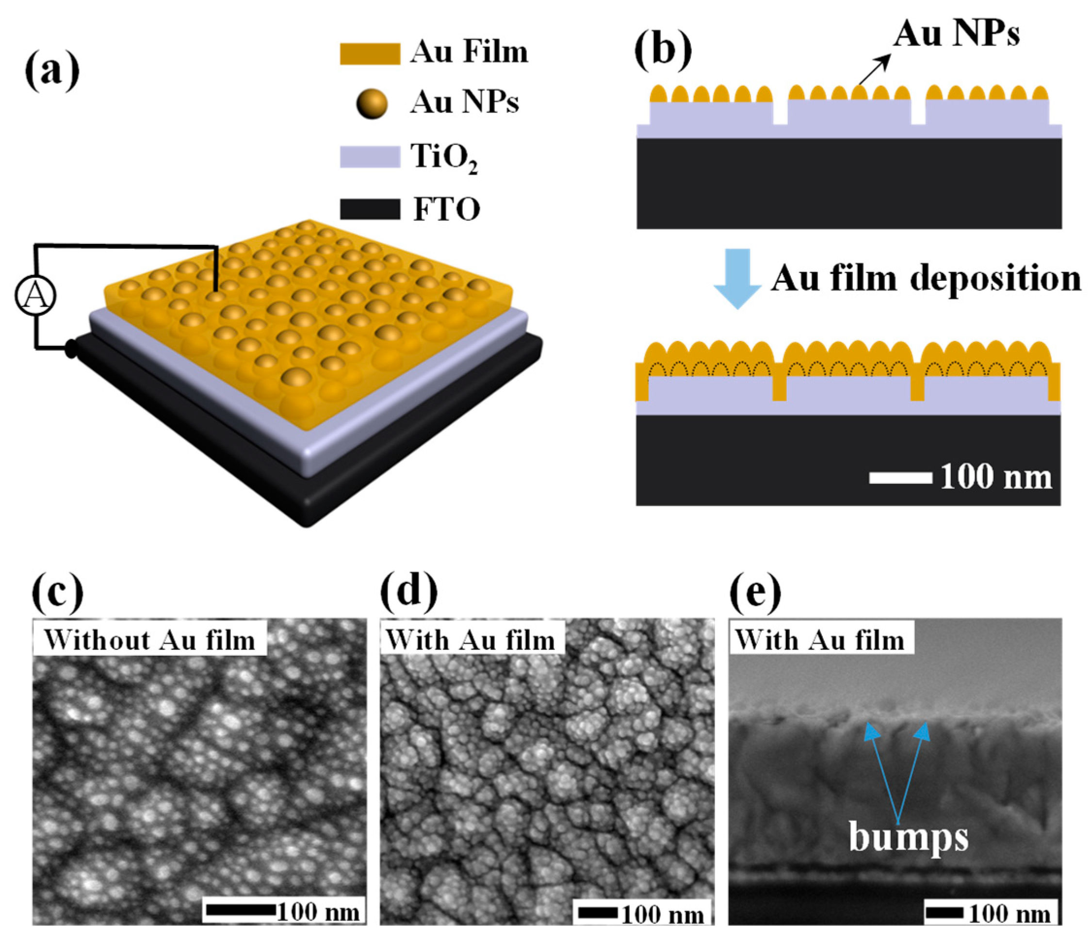
2. Structure and Experimental Details
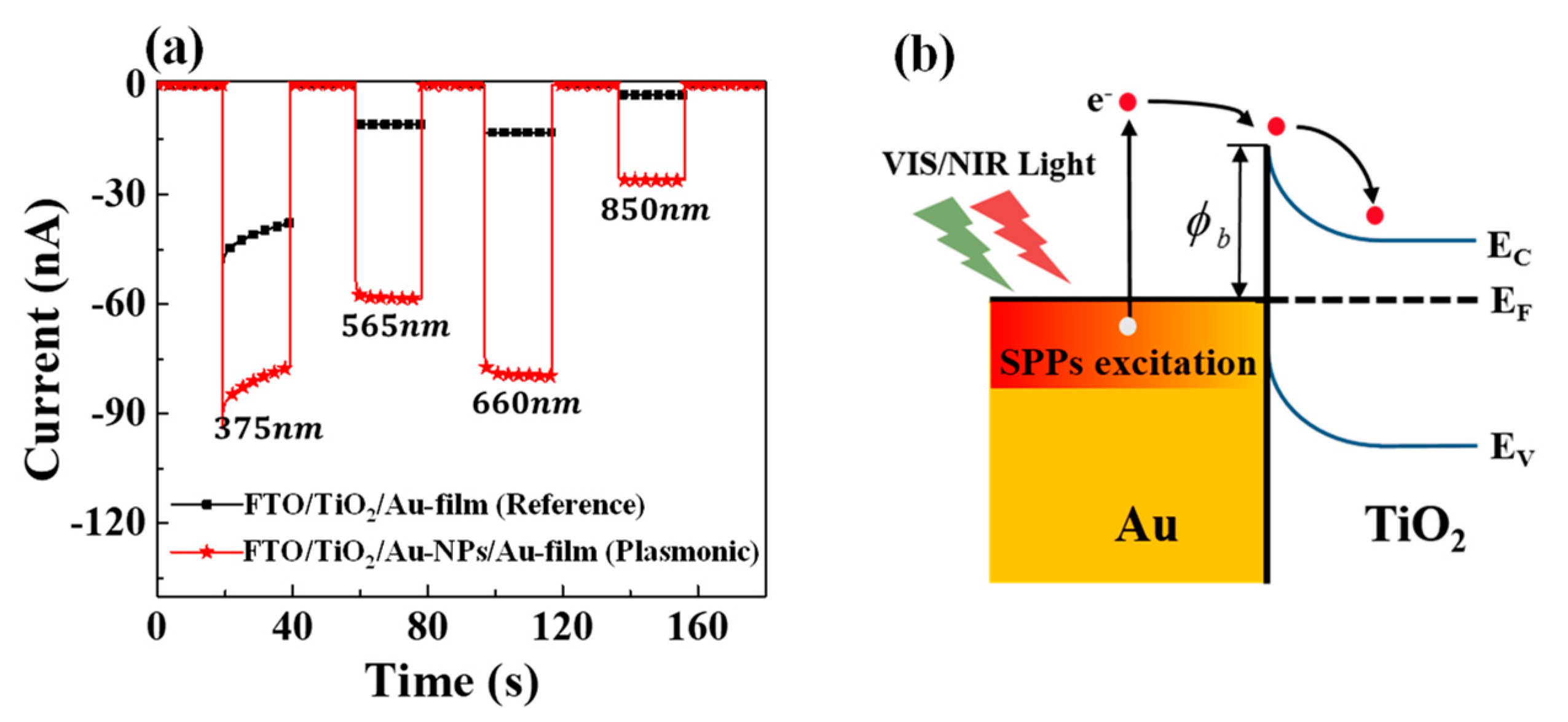
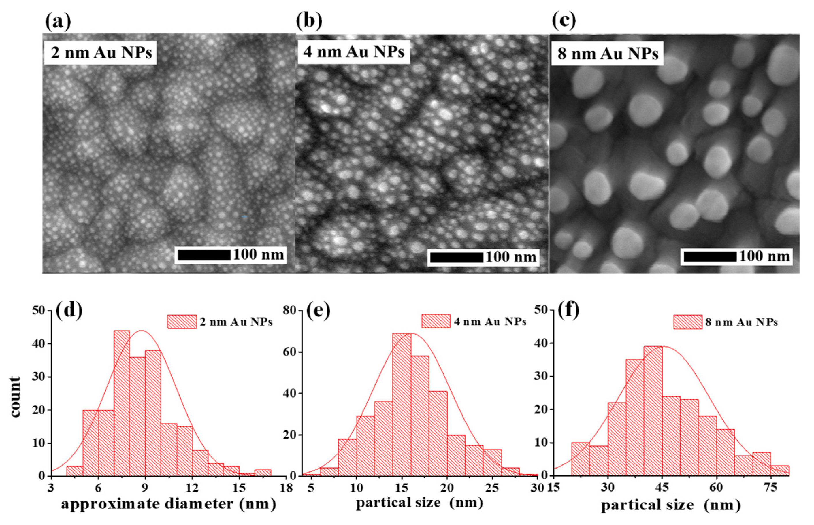
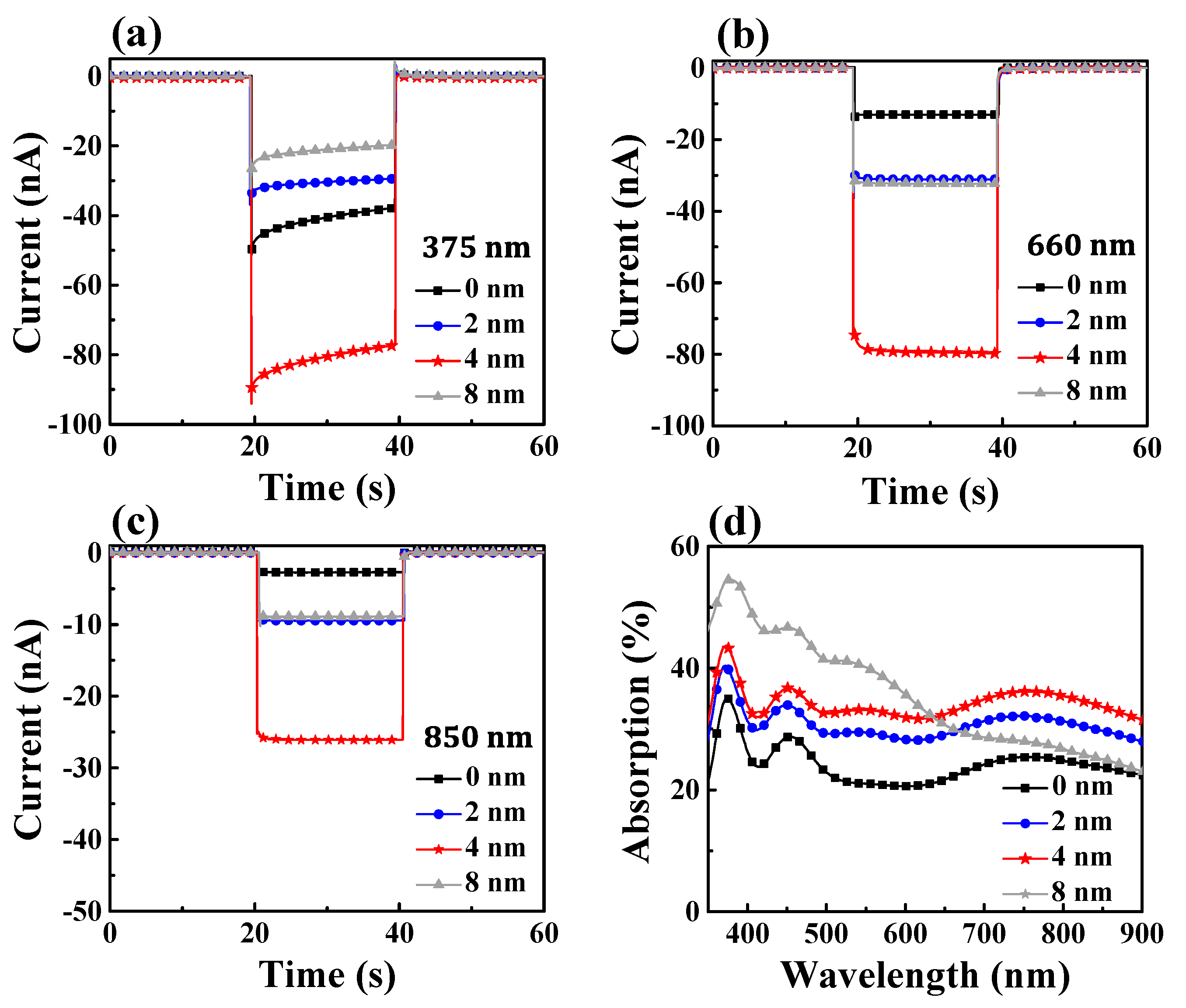
3. Results and Discussions
4. Conclusions
Supplementary Materials
Author Contributions
Funding
Institutional Review Board Statement
Informed Consent Statement
Data Availability Statement
Acknowledgments
Conflicts of Interest
References
- Shao, W.; Yang, Q.; Zhang, C.; Wu, S.; Li, X. Planar dual-cavity hot-electron photodetectors. Nanoscale 2019, 11, 1396–1402. [Google Scholar] [CrossRef] [PubMed]
- Zhang, C.; Qian, Q.; Qin, L.; Zhu, X.; Wang, C.; Li, X. Broadband Light Harvesting for Highly Efficient Hot-Electron Application Based on Conformal Metallic Nanorod Arrays. ACS Photonics 2018, 5, 5079–5085. [Google Scholar] [CrossRef]
- Tanzid, M.; Ahmadivand, A.; Zhang, R.; Cerjan, B.; Sobhani, A.; Yazdi, S.; Nordlander, P.; Halas, N.J. Combining Plasmonic Hot Carrier Generation with Free Carrier Absorption for High-Performance Near-Infrared Silicon-Based Photodetection. ACS Photonics 2018, 5, 3472–3477. [Google Scholar] [CrossRef]
- Mirzaee, S.M.A.; Lebel, O.; Nunzi, J.M. Simple Unbiased Hot-Electron Polarization-Sensitive Near-Infrared Photodetector. ACS Appl. Mater. Int. 2018, 10, 11862–11871. [Google Scholar] [CrossRef]
- Luo, X.; Zhao, F.; Liang, Y.; Du, L.; Lv, W.; Xu, K.; Wang, Y.; Peng, Y. Facile Nanogold-Perovskite Enabling Ultrasensitive Flexible Broadband Photodetector with pW Scale Detection Limit. Adv. Opt. Mater. 2018, 6, 1800996. [Google Scholar] [CrossRef]
- Yao, K.; Zhong, H.; Liu, Z.; Xiong, M.; Leng, S.; Zhang, J.; Xu, Y.; Wang, W.; Zhou, L.; Huang, H.; et al. Plasmonic metal nanoparticles with core-bishell structure for high-performance organic and perovskite solar cells. ACS Nano 2019, 13, 5397–5409. [Google Scholar] [CrossRef]
- Wang, W.; Cui, Y.; Fung, K.; Zhang, Y.; Ji, T.; Hao, Y. Comparison of Nanohole-Type and Nanopillar-Type Patterned Metallic Electrodes Incorporated in Organic Solar Cells. Nanoscale Res. Lett. 2017, 12, 538. [Google Scholar] [CrossRef] [Green Version]
- Kumar, K.V.; Goud, J.P.; Kumar, K.R.; Raju, K.; Rao, S. Laser annealing of Au/HfO2 bi-layers to fabricate Au nanoparticles without altering the phase of HfO2 for applications in SERS and memory devices. J. Mater. Sci.-Mater. Electron. 2022, 33, 6657–6669. [Google Scholar] [CrossRef]
- Ishii, S.; Shinde, S.L.; Nagao, T. Nonmetallic Materials for Plasmonic Hot Carrier Excitation. Adv. Opt. Mater. 2019, 7, 1800603. [Google Scholar] [CrossRef] [Green Version]
- Jang, Y.J.; Chung, K.; Lee, J.S.; Choi, C.H.; Lim, J.W.; Kim, D.H. Plasmonic Hot Carriers Imaging: Promise and Outlook. ACS Photonics 2018, 5, 4711–4723. [Google Scholar] [CrossRef]
- Ho, Y.-L.; Tai, Y.-H.; Clark, J.K.; Wang, Z.; Wei, P.-K.; Delaunay, J.-J. Plasmonic Hot-Carriers in Channel-Coupled Nanogap Structure for Metal–Semiconductor Barrier Modulation and Spectral-Selective Plasmonic Monitoring. ACS Photonics 2018, 5, 2617–2623. [Google Scholar] [CrossRef]
- Zayats, A.V.; Maier, S. Hot-Electron Effects in Plasmonics and Plasmonic Materials. Adv. Opt. Mater. 2017, 5, 1700508. [Google Scholar] [CrossRef] [Green Version]
- Li, W.; Valentine, J.G. Harvesting the loss: Surface plasmon-based hot electron photodetection. Nanophotonics 2017, 6, 177–191. [Google Scholar] [CrossRef]
- Tagliabue, G.; Jermyn, A.S.; Sundararaman, R.; Welch, A.J.; DuChene, J.S.; Pala, R.; Davoyan, A.R.; Narang, P.; Atwater, H.A. Quantifying the role of surface plasmon excitation and hot carrier transport in plasmonic devices. Nat. Commun. 2018, 9, 3394. [Google Scholar] [CrossRef] [Green Version]
- Lee, C.; Choi, H.; Nedrygailov, I.I.; Lee, Y.K.; Jeong, S.; Park, J.Y. Enhancement of Hot Electron Flow in Plasmonic Nanodiodes by Incorporating PbS Quantum Dots. ACS Appl. Mater. Int. 2018, 10, 5081–5089. [Google Scholar] [CrossRef]
- Ratchford, D.C.; Dunkelberger, A.D.; Vurgaftman, I.; Owrutsky, J.C.; Pehrsson, P.E. Quantification of Efficient Plasmonic Hot-Electron Injection in Gold Nanoparticle–TiO2 Films. Nano Lett. 2017, 17, 6047–6055. [Google Scholar] [CrossRef]
- Mupparapu, R.; Cunha, J.; Tantussi, F.; Jacassi, A.; Summerer, L.; Patrini, M.; Giugni, A.; Maserati, L.; Alabastri, A.; Garoli, D.; et al. High-Frequency Light Rectifcation by Nanoscale Plasmonic Conical Antenna in Point-Contact-Insulator-Metal Architecture. Adv. Energy Mater. 2022, 2103785. [Google Scholar] [CrossRef]
- Yang, Z.; Du, K.; Wang, H.; Lu, F.; Pang, Y.; Wang, J.; Gan, X.; Zhang, W.; Mei, T.; Chua, S.J. Near-infrared photodetection with plasmon-induced hot electrons using silicon nanopillar array structure. Nanotechnology 2019, 30, 075204. [Google Scholar] [CrossRef]
- Scales, C.; Berini, P. Thin-Film Schottky Barrier Photodetector Models. IEEE J. Quantum Electron. 2010, 46, 633–643. [Google Scholar] [CrossRef]
- Scales, C.; Breukelaar, I.; Berini, P. Surface-plasmon Schottky contact detector based on a symmetric metal stripe in silicon. Opt. Lett. 2010, 35, 529–531. [Google Scholar] [CrossRef]
- Zhang, C.; Wu, K.; Giannini, V.; Li, X. Planar Hot-Electron Photodetection with Tamm Plasmons. ACS Nano 2017, 11, 1719–1727. [Google Scholar] [CrossRef] [PubMed] [Green Version]
- Ouyang, W.; Teng, F.; Jiang, M.; Fang, X. ZnO Film UV Photodetector with Enhanced Performance: Heterojunction with CdMoO4 Microplates and the Hot Electron Injection Effect of Au Nanoparticles. Small 2017, 13, 1702177. [Google Scholar] [CrossRef] [PubMed]
- Zhang, C.; Wu, K.; Ling, B.; Li, X. Conformal TCO-semiconductor-metal nanowire array for narrowband and polarization-insensitive hot-electron photodetection application. J. Photonics Energy 2016, 6, 042502. [Google Scholar] [CrossRef]
- Zhang, Q.; Zhang, C.; Qin, L.; Li, X. Polarization-insensitive hot-electron infrared photodetection by double Schottky junction and multilayer grating. Opt. Lett. 2018, 43, 3325–3328. [Google Scholar] [CrossRef]
- Nusir, A.I.; Abbey, G.P.; Hill, A.M.; Manasreh, O.; Herzog, J.B. Hot Electrons in Microscale Thin-Film Schottky Barriers for Enhancing Near-Infrared Detection. IEEE Photonics Technol. Lett. 2016, 28, 2241–2244. [Google Scholar] [CrossRef]
- Knight, M.W.; Wang, Y.; Urban, A.S.; Sobhani, A.; Zheng, B.Y.; Nordlander, P.; Halas, N.J. Embedding plasmonic nanostructure diodes enhances hot electron emission. Nano Lett. 2013, 13, 1687–1692. [Google Scholar] [CrossRef]
- Wu, K.; Zhan, Y.; Zhang, C.; Wu, S.; Li, X. Strong and highly asymmetrical optical absorption in conformal metal-semiconductor-metal grating system for plasmonic hot-electron photodetection application. Sci. Rep. 2015, 5, 14304. [Google Scholar] [CrossRef] [Green Version]
- Feng, B.; Zhu, J.; Lu, B.; Liu, F.; Zhou, L.; Chen, Y. Achieving Infrared Detection by All-Si Plasmonic Hot-Electron Detectors with High Detectivity. ACS Nano 2019, 13, 8433–8441. [Google Scholar] [CrossRef]
- Chen, W.; Lu, Y.; Dong, W.; Chen, Z.; Shen, M. Plasmon mediated visible light photocurrent and photoelectrochemical hydrogen generation using au nanoparticles/TiO2 electrode. Mater. Res. Bull. 2014, 50, 31–35. [Google Scholar] [CrossRef]
- Lu, Y.; Dong, W.; Chen, Z.; Pors, A.; Wang, Z.; Bozhevolnyi, S.I. Gap-plasmon based broadband absorbers for enhanced hot-electron and photocurrent generation. Sci. Rep. 2016, 6, 30650. [Google Scholar] [CrossRef] [Green Version]
- Qi, Z.; Zhai, Y.; Wen, L.; Wang, Q.; Chen, Q.; Iqbal, S.; Chen, G.; Xu, J.; Tu, Y. Au nanoparticle-decorated silicon pyramids for plasmon-enhanced hot electron near-infrared photodetection. Nanotechnology 2017, 28, 275202. [Google Scholar] [CrossRef] [PubMed]
- Hoang, C.V.; Hayashi, K.; Ito, Y.; Gorai, N.; Allison, G.; Shi, X.; Sun, Q.; Cheng, Z.; Ueno, K.; Goda, K.; et al. Interplay of hot electrons from localized and propagating plasmons. Nat. Commun. 2017, 8, 771. [Google Scholar] [CrossRef] [PubMed]
- Fang, Y.; Jiao, Y.; Xiong, K.; Ogier, R.; Yang, Z.J.; Gao, S.; Dahlin, A.B.; Kall, M. Plasmon Enhanced Internal Photoemission in Antenna-Spacer-Mirror Based Au/TiO2 Nanostructures. Nano Lett. 2015, 15, 4059–4065. [Google Scholar] [CrossRef] [PubMed]
- Liang, F.-X.; Wang, J.-Z.; Wang, Y.; Lin, Y.; Liang, L.; Gao, Y.; Luo, L.-B. Single-layer graphene/titanium oxide cubic nanorods array/FTO heterojunction for sensitive ultraviolet light detection. Appl. Surf. Sci. 2017, 426, 391–398. [Google Scholar] [CrossRef]

Publisher’s Note: MDPI stays neutral with regard to jurisdictional claims in published maps and institutional affiliations. |
© 2022 by the authors. Licensee MDPI, Basel, Switzerland. This article is an open access article distributed under the terms and conditions of the Creative Commons Attribution (CC BY) license (https://creativecommons.org/licenses/by/4.0/).
Share and Cite
Wang, W.; Zhang, C.; Qiu, K.; Li, G.; Zhai, A.; Hao, Y.; Li, X.; Cui, Y. Enhancing Hot-Electron Photodetection of a TiO2/Au Schottky Junction by Employing a Hybrid Plasmonic Nanostructure. Materials 2022, 15, 2737. https://doi.org/10.3390/ma15082737
Wang W, Zhang C, Qiu K, Li G, Zhai A, Hao Y, Li X, Cui Y. Enhancing Hot-Electron Photodetection of a TiO2/Au Schottky Junction by Employing a Hybrid Plasmonic Nanostructure. Materials. 2022; 15(8):2737. https://doi.org/10.3390/ma15082737
Chicago/Turabian StyleWang, Wenyan, Cheng Zhang, Kaifang Qiu, Guohui Li, Aiping Zhai, Yuying Hao, Xiaofeng Li, and Yanxia Cui. 2022. "Enhancing Hot-Electron Photodetection of a TiO2/Au Schottky Junction by Employing a Hybrid Plasmonic Nanostructure" Materials 15, no. 8: 2737. https://doi.org/10.3390/ma15082737
APA StyleWang, W., Zhang, C., Qiu, K., Li, G., Zhai, A., Hao, Y., Li, X., & Cui, Y. (2022). Enhancing Hot-Electron Photodetection of a TiO2/Au Schottky Junction by Employing a Hybrid Plasmonic Nanostructure. Materials, 15(8), 2737. https://doi.org/10.3390/ma15082737