Article

Broadband Perfect Absorber in the Visible Range Based on Metasurface Composite Structures

1
Microelectronics Instruments and Equipments R&D Center, Institute of Microelectronics of Chinese Academy of Sciences, Beijing 100029, China
2
School of Microelectronics, University of Chinese Academy of Sciences, Beijing 101499, China
*
Author to whom correspondence should be addressed.
Materials 2022, 15(7), 2612; https://doi.org/10.3390/ma15072612
Submission received: 9 March 2022 / Revised: 27 March 2022 / Accepted: 31 March 2022 / Published: 1 April 2022

Abstract

:
The broadband perfect absorption of visible light is of great significance for solar cells and photodetectors. The realization of a two-dimensional broadband perfect absorber in the visible range poses a formidable challenge with regard to improving the integration of optical systems. In this paper, we numerically demonstrate a broadband perfect absorber in the visible range from 400 nm to 700 nm based on metasurface composite structures. Simulation results show that the average absorptance is ~95.7% due to the combination of the intrinsic absorption of the lossy metallic material (Au) and the coupling resonances of the multi-sized resonators. The proposed perfect absorber may find potential applications in photovoltaics and photodetection.

1. Introduction

A broadband perfect absorber in the visible range has great potential for solar energy harvesting [1,2,3] and photoelectric detection [4,5]. Naturally occurring materials, such as organic dyes and inorganic pigments, usually exhibit insufficient absorption in the visible range for many modern photonic applications [6]. Metamaterials are made up of artificially subwavelength nanostructures, providing numerous unconventional optical properties [7]. Their electromagnetic properties can be easily adjusted by the size and geometry of the nanostructures. Based on the impedance match between the designed metamaterial and the free space, the first metamaterial perfect absorber was demonstrated in 2008 in the microwave band [8]. Since then, the perfect absorber has been extended to the terahertz [9,10,11], mid-infrared [12], infrared [13,14,15], and visible range [16,17,18].
The bandwidth of an absorber is important for many scientific and technical applications. The narrowband absorbers are quite important for sensing applications, such as temperature or refractive index sensing, absorption filtering, and optical signal processing [19,20,21]. On the other hand, broadband absorbers facilitate seminal applications encompassing photovoltaic cells and optoelectronic detectors. The reported scheme for an broadband absorber based on metamaterials mainly relies on multiple vertically layered metamaterials [22,23,24]. However, due to the laminated structures, the reported absorbers are bulky and complex for use in fabrication. The realization of an ultrathin broadband perfect absorber is of great significance for integration applications. Metasurfaces comprise subwavelength constituent elements within an optically thin layer that can alter the amplitude, phase, and polarization of an incident electromagnetic wave [25,26]. The development of metasurfaces provides a unique opportunity for the planarization and miniaturization of the broadband perfect absorber [27,28]. Two-dimensional broadband perfect absorbers with a horizontal arrangement of several resonators in different sizes were obtained [29,30]. However, the absorption spectrum usually consists of several discrete peaks and the average absorption achieved is not high enough. Additionally, the use of a perfect absorber with a continuous broad bandwidth in the visible range is more favorable for many practical applications.
In this paper, a broadband perfect absorber based on metasurface composite structures in the visible range is demonstrated. The simulation results illustrate that the perfect absorber yields a ~95.7% average absorptance in the visible range (400–700 nm). The perfect absorption mechanism lies in the combination of the intrinsic absorption of the gold material (400 nm–550 nm) and the coupling resonances of multi-sized resonators (550 nm–700 nm) according to the simulation. Given the broad absorption bandwidth, high absorptance, and ultrathin structure, the designed metasurface absorbers may find potential applications in solar cells [31,32] and photodetection [33,34].

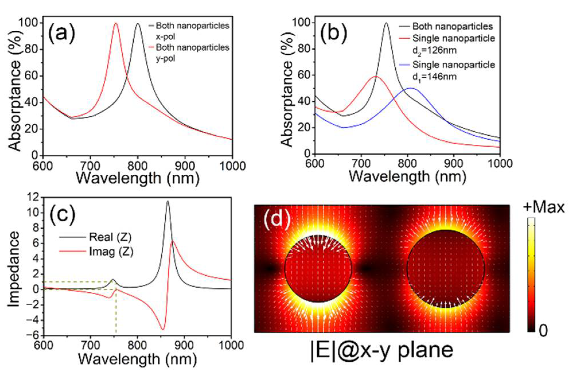
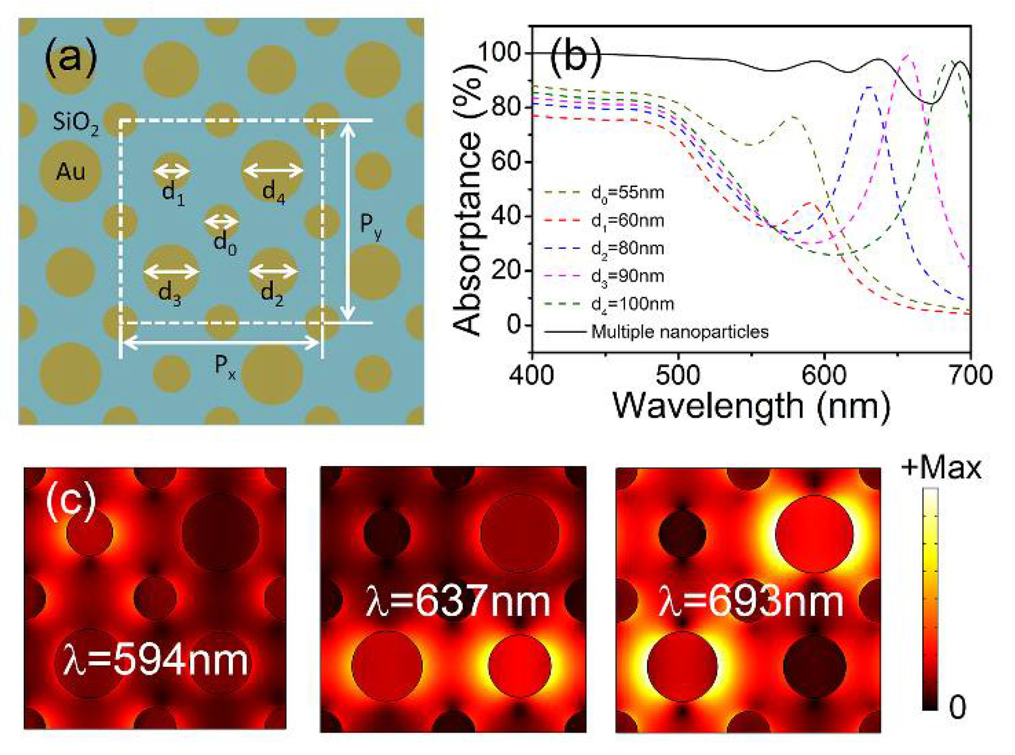
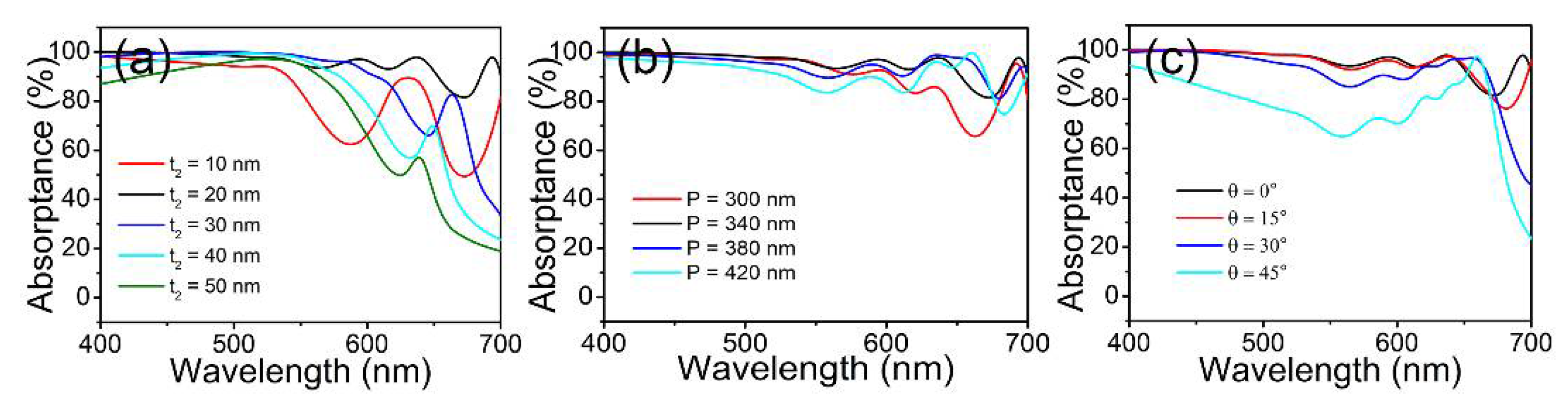
2. Simulation and Discussion

As plotted in Figure 1a, the unit cell of a metasurface is a metal–insulator–metal (MIM) sandwich structure. This consists of a circular-shaped gold nanoparticle and a gold substrate separated by a silicon dioxide (SiO2) spacer. The thicknesses of nanoparticles, SiO2 layer, and gold substrate are t1 = 30 nm, t2 = 50 nm, and t3 = 100 nm, respectively. The lateral dimension is Λ = 240 nm. The metasurface composite structures consist of two differently sized nanoparticles with diameters of d1 = 146 nm and d2 = 126 nm. Figure 1b plots the top view of the metasurface composite structures with periods of Px = 2Λ = 480 nm and Py = Λ = 240 nm. The absorption characteristics of the metasurface composite structures are simulated using the COMSOL Multiphysics V5.4 (2018, Stockholm, Sweden) with periodic boundary conditions. The refractive index of the SiO2 is 1.45 and the permittivity of gold as a function of the incident wavelength is taken from the experimental results [35]. The perfect absorption is obtained based on the parameter optimization of the diameters of the gold nanoparticles. The simulated absorption spectra of the metasurface composite structures (with both nanoparticles, black solid curve) and the absorption spectra of each constituent nanoparticle (red solid curve for d2 = 126 nm and blue solid curve for d1 = 146 nm) are plotted in Figure 1c under x polarization. For the metasurface composite structures with both nanoparticles, the absorptance is ~99.64% and the bandwidth ΔλFWHM (full width at half maximum) is 67 nm at the resonant wavelength of λres = 800 nm. For the metasurface structures with a single nanoparticle of d2 = 126 nm, the absorptance is ~67.16% and ΔλFWHM = 98 nm at λres = 760 nm. For the metasurface structures with a single nanoparticle of d1 = 146 nm, the absorptance is ~57.18% and ΔλFWHM = 131 nm at λres = 820 nm.
The absorptance A λ is obtained from A λ = 1 T λ R λ . T λ is transmittance, while R λ is reflectance. The transmittance T λ is zero since the thickness of the gold substrate is t3 = 100 nm, which is greater than the skin depth of the gold film. As a result, A λ = 1 R λ . The reflectance can be minimized until zero under the condition of impedance matching, resulting in the perfect absorption of A λ ~ 100   % . The impedance Z of the metasurface composite structures can be calculated according to the following equation [36]:
Z = 1 + S 11 2 S 21 2 1 S 11 2 S 21 2
Here, S11 is the complex reflection coefficient while S21 denotes the complex transmission coefficient. Due to the optical thickness of the gold substrate, S21 is zero. The simulated real and imaginary parts of the impedance are presented in Figure 1d. The real part is 1 and the imaginary part is 0 at the resonant wavelength of 800 nm; both of these are perfectly matched to the vacuum values and result in a perfect absorption effect.
To illuminate the absorption mechanism, the norm of the electric field (|E|, color plot) and the local electric field distribution at each position (white arrows) in the x–y plane through the nanoparticles 15 nm above the SiO2 layer and the x–z plane are plotted in Figure 1e,f under x polarization at the resonant wavelength of 800 nm. |E| shows that strong coupling exists between the two nanoparticles, and the absorption spectrum of the metasurface composite structures with both nanoparticles can be viewed as a coupling superposition of the absorption spectrum of each constituent nanoparticle. The white arrows indicate that the electric dipole resonance is excited in the nanoparticles when an x-polarized incident beam normally reaches the metasurface composite structures. Meanwhile, the norms of the magnetic field (|H|, color plot) and the electric current (white arrows) of the metasurface composite structures in the x–z plane are shown in Figure 1g. The antiparallel electric currents are induced in both the gold nanoparticles and substrate, and a strong magnetic dipole resonance is generated in the thin SiO2 layer [37]. As a result, impedance matching and the perfect absorption effect can be obtained at the resonance wavelength [38].
Figure 2a plots the simulated absorption spectra of the metasurface composite structures under x and y polarizations with the resonant wavelengths of 800 nm and 754 nm, respectively. For y-polarized incidence, the absorption spectra of the metasurface composite structures with both nanoparticles (black solid curve) and with each constituent nanoparticle (red solid curve for d2 = 126 nm and blue solid curve for d1 = 146 nm) are simulated in Figure 2b. For the metasurface composite structures with both nanoparticles, the absorptance is ~99.95% and ΔλFWHM = 64 nm at λres = 754 nm. The absorptance is ~59.08% and ΔλFWHM = 153 nm at λres = 731 nm for the metasurface structures with a single nanoparticle of d2 = 126 nm. As for the metasurface structures with a single nanoparticle of d1 = 146 nm, the absorptance is ~50.23% and ΔλFWHM = 170 nm at λres = 806 nm. The impedance is simulated in Figure 2c. The real and imaginary parts are perfectly matched to the vacuum values at λres = 754 nm. Figure 2d plots the norm of the electric field (|E|, color plot) and local electric field distribution (white arrows) in the x–y plane through the nanoparticles 15 nm above the SiO2 layer at λres = 754 nm. The electric dipole resonance can be easily observed in the nanoparticles. It is found that there is no strong coupling between the two nanoparticles, and the absorption spectrum of the metasurface composite structures with both nanoparticles can be viewed as a simple superposition of the absorption spectrum of each constituent nanoparticle.
The comparison between Figure 1c and Figure 2a shows that the perfect absorption characteristics are polarization-dependent because of the asymmetry of the geometry along the x- and y-axes. To improve the polarization dependence, the metasurface composite structures are designed with four diagonal symmetric gold nanoparticles above the SiO2 layer, as shown in Figure 3a. The geometrical parameters are d1 = 146 nm, d2 = 126 nm, and Px = Py = 2Λ = 480 nm, respectively. The thicknesses of the nanoparticles (t1), SiO2 layer (t2), and gold substrate (t3) are the same as those in Figure 1a. The simulated polarization-insensitive absorption spectra are presented in Figure 3b under x (black dashed curve) and y (red dotted curve) polarization. The absorptance is ~95.88% and the ΔλFWHM is 55 nm at λres = 745 nm. The norms of the electric field (|E|, color plot) and local electric field distributions (white arrows) of the metasurface composite structures in the x–y plane are plotted in Figure 3c,d under x polarization and y polarization at λres = 745 nm. The electric dipole resonances can be separately observed along the x-axis and y-axis. It can be seen that, due to the symmetry of the composite structure, the absorption spectra under x- and y-polarization are identical, indicating the polarization insensitivity of the composite structure.
To achieve the perfect absorption in a broader wavelength range, five differently sized nanoparticles were designed in the metasurface composite structures, as plotted in Figure 4a. The diameters of the gold nanoparticles were optimized as d0 = 55 nm, d1 = 60 nm, d2 = 80 nm, d3 =90 nm, and d4 = 100 nm, respectively. The thicknesses of the nanoparticles, SiO2 layer, and gold substrate were t1 = 30 nm, t2 = 20 nm, and t3 = 100 nm, respectively. The subwavelength lateral dimension was reduced to Λ =160 nm to minimize the influence of the diffraction effects. As a result, the period was Px = Py = 2Λ = 320 nm. The absorption spectra were simulated (as presented in Figure 4b) under x-polarized incident light (black solid curve). It can be observed that the absorptance was beyond 90% in the wavelength ranges of 400–650 nm and 685–700 nm. For the broad visible wavelength range of 400–700 nm, the average absorptance was ~95.7%. Additionally, to illustrate the perfect absorption mechanism, the absorption spectra of the metasurface comprising each constituent gold nanoparticle were simulated (as plotted in Figure 4b) with diameters of 55, 60, 80, 90, and 100 nm. This was achieved by setting only one nanoparticle as a Au nanoparticle and all other nanoparticles as air in each simulation; this procedure was repeated for all constituent nanoparticles. The spectra exhibited pronounced resonance peaks at wavelengths of 580, 590, 630, 657, and 685 nm with absorptance values of 76.6%, 45.0%, 87.9%, 99.2%, and 97.3%, respectively. The resonant wavelengths were redshifted with the increase in the diameters of the nanoparticles. The power loss accumulated at the resonant wavelengths, where the energy of the incident light was converted into heat, resulting in a high level of absorption. As the designed five adjacent resonance peaks were so close, they could couple with each other and merge into a broad absorption band (550–700 nm). Meanwhile, the absorption in the shorter wavelength (400–550 nm) originated from the intrinsic absorption of the gold material, with an absorptance close to unity. The finite-element simulations shown in Figure 4c further verify the broadband perfect absorption mechanism in the range of 550–700 nm. The norm of the electric field (|E|, color plot) was plotted in the x–y plane through the nanoparticles 15 nm above the SiO2 layer under x-polarized incident lights. The coupled electric dipole resonances were observed at the different resonance peaks of 594 nm, 637 nm, and 693 nm according to the absorption spectra of the metasurface composite structures with multiple nanoparticles (black solid curve in Figure 4a). It can be observed that the broadband absorption in the range of 550–700 nm originated from the superposition of the coupling resonances of the multi-sized nanoparticles.
Subsequently, the influence of geometrical parameters on the proposed perfect absorber was investigated. Figure 5a plots the absorption spectra with respect to the thickness of the SiO2 layer t2. The average absorptance was 82.8%, 95.7%, 88.2%, 80.2%, and 73.2% when t2 = 10 nm, 20 nm, 30 nm, 40 nm, and 50 nm, respectively. On the other hand, the absorption spectra are presented in Figure 5b as functions of the period P. The average absorptance was 91.5%, 95.7%, 94.7%, and 91.3% when P = 300 nm, 340 nm, 380 nm, and 420 nm, respectively. It can be seen that the optimized perfect absorption was obtained when t2 = 20 nm and P = 340 nm, which is in accordance with the geometrical parameters shown in Figure 4. In addition, the absorption dependence at oblique incidence is illustrated in Figure 5c. Compared with the normal incidence (θ = 0°), the average absorptance decreased to 94.9%, 90.3%, and 75.6% when θ = 15°, 30°, and 45°, respectively. It can be observed that the broadband perfect absorption performance could be maintained when the incident angle increased up to 30°.
The anticipated fabrication of the proposed perfect absorber was based on the standard electron beam lithography steps [39]. Firstly, gold film with a thickness of 100 nm was deposited on a silicon substrate using electron beam evaporation. Secondly, a silicon dioxide film with an optimized thickness was formed by chemical vapor deposition. Finally, an array of multi-sized gold nanoparticles was fabricated using electron beam lithography, metal deposition, and a lift-off process. Based on high-resolution electron beam lithography (EBL) with a negative-tone hydrogen silsesquioxane (HSQ) resist and the lift-off process [40,41], gold nanoparticles with different-sized diameters could be reliably fabricated to satisfy the designed structural parameters (e.g., d0 = 55 nm, d1 = 60 nm, d2 = 80 nm, d3 =90 nm, and d4 = 100 nm). Additionally, the absorption mechanism (the material intrinsic absorption and the coupling resonances of the multi-sized resonators) allows for a relaxed tolerance of the nanoparticle diameters in practical fabrication on the condition that the diameters are evenly distributed within a certain range (from 55 nm to 100 nm). Slight deviations from the original diameter may lead to a shift in a single absorption peak, but the broadband absorption effect will remain.

3. Conclusions

In conclusion, in this research a broadband perfect absorber was proposed and numerically studied in the visible range based on metasurface composite structures. The simulated average absorptance was ~95.7% under x polarization in the wavelength range of 400–700 nm. The intrinsic absorption of gold material contributed to the absorption in the range of 400 to 550 nm, and the superposition of multiple resonances of composite nanoparticles contributed to the absorption in the range of 550 to 700 nm. A systematic strategy for the structure of broadband perfect absorbers was thus established. Based on the geometry scalability, the perfect absorber may operate at other wavelength ranges. Given their broad spectral absorption range and high absorptance, the designed metasurface absorbers may find potential applications in enhancing photovoltaics and photodetection.

Author Contributions

Conceptualization, R.W.; methodology, S.Y.; software, Z.Z. (Zhe Zhang); validation, H.Z. and S.Q.; formal analysis, S.Y. and Y.H.; data curation, R.W. and M.L.; writing—original draft preparation, R.W.; writing—review and editing, S.Y. and Z.Z. (Zichen Zhang); project administration, Z.Z. (Zichen Zhang); funding acquisition, S.Y. and Z.Z. (Zichen Zhang). All authors have read and agreed to the published version of the manuscript.

Funding

This research was funded by Beijing Natural Science Foundation (grant number 4224097), Youth Innovation Promotion Association CAS (grant number 2021114), Scientific Research Equipment Project of Chinese Academy of Sciences (grant number YJKYYQ20210052), Beijing Nova Programs of Science and Technology (grant numbers Z211100002121124 and Z191100001119058) and National Natural Science Foundation of China (grant number 61905273).

Institutional Review Board Statement

Not applicable.

Data Availability Statement

Not applicable.

Conflicts of Interest

The authors declare no conflict of interest.

References

  1. Patel, S.K.; Charola, S.; Jani, C.; Ladumor, M.; Guo, T. Graphene-based highly efficient and broadband solar absorber. Opt. Mater. 2019, 96, 109330. [Google Scholar] [CrossRef]
  2. Zhou, J.; Liu, Z.; Liu, G.; Pan, P.; Wang, J. Ultra-broadband solar absorbers for high-efficiency thermophotovoltaics. Opt. Express 2020, 28, 36476. [Google Scholar] [CrossRef] [PubMed]
  3. Park, S.; Heo, S.W.; Lee, W.; Inoue, D.; Zhi, J.; Yu, K.; Jinno, H.; Hashizume, D.; Sekino, M.; Yokota, T.; et al. Self-powered ultra-flexible electronics via nano-grating-patterned organic photovoltaics. Nature 2018, 561, 516–521. [Google Scholar] [CrossRef] [PubMed]
  4. Zheng, B.Y.; Wan, Y.; Nordlander, P.; Halas, N.J. Color-Selective and CMOS-Compatible Photodetection Based on Aluminum Plasmonics. Adv. Mater. 2014, 26, 6318–6323. [Google Scholar] [CrossRef] [PubMed]
  5. Suen, J.Y.; Fan, F.; Montoya, J.; Bingham, C.; Padilla, W.J. Multifunctional metamaterial pyroelectric infrared detectors. Optica 2017, 4, 276–279. [Google Scholar] [CrossRef]
  6. Talghader, J.J.; Gawarikar, A.S.; Shea, R.P. Spectral selectivity in infrared thermal detection. Light Sci. App. 2012, 1, e24. [Google Scholar] [CrossRef] [Green Version]
  7. Mcphedran, R.C.; Shadrivov, I.V.; Kuhlmey, B.T.; Kivshar, Y.S. Metamaterials and metaoptics. NPG Asia Mater. 2011, 3, 100–108. [Google Scholar] [CrossRef]
  8. Landy, N.; Sajuyigbe, S.; Mock, J.; Smith, D.; Padilla, W. Perfect metamaterial absorber. Phys. Rev. Lett. 2008, 100, 207402. [Google Scholar] [CrossRef]
  9. Meng, W.; Zhao, X.; Zhang, J.; Schalch, J.; Xin, Z. A three-dimensional all-metal terahertz metamaterial perfect absorber. Appl. Phys. Lett. 2017, 111, 051101. [Google Scholar] [CrossRef]
  10. Jia, D.; Xu, J.; Yu, X. Ultra-broadband terahertz absorption using bi-metasurfaces based multiplexed resonances. Opt. Express 2018, 26, 26227–26234. [Google Scholar] [CrossRef]
  11. Zhou, R.; Jiang, T.; Peng, Z.; Li, Z.; Su, H. Tunable broadband terahertz absorber based on graphene metamaterials and VO2. Opt. Mater. 2021, 114, 110915. [Google Scholar] [CrossRef]
  12. Liang, Y.; Koshelev, K.; Zhang, F.; Lin, H.; Kivshar, Y. Bound states in the continuum in anisotropic plasmonic metasurfaces. Nano Lett. 2020, 20, 6351–6356. [Google Scholar] [CrossRef] [PubMed]
  13. Liu, N.; Mesch, M.; Weiss, T.; Hentschel, M.; Giessen, H. Infrared perfect absorber and its application as plasmonic sensor. Nano Lett. 2010, 10, 2342–2348. [Google Scholar] [CrossRef] [PubMed]
  14. Zhang, F.; Wang, Q.; Ding, L. Broadband near-infrared metamaterial absorber based on rainbow trapping effect. Opt. Commun. 2020, 475, 126284. [Google Scholar] [CrossRef]
  15. Parsamyan, H. Near-Perfect Broadband Infrared Metamaterial Absorber Utilizing Nickel. Appl. Optics 2020, 59, 7504–7509. [Google Scholar] [CrossRef] [PubMed]
  16. Akselrod, G.M.; Huang, J.; Hoang, T.B.; Bowen, P.T.; Su, L.; Smith, D.R.; Mikkelsen, M.H. Large-Area Metasurface Perfect Absorbers from Visible to Near-Infrared. Adv. Mater. 2015, 27, 7897–8115. [Google Scholar] [CrossRef]
  17. Zhou, Y.; Lu, M.; Chen, L. Polarization-Independent Near-Perfect Absorber in the Visible Regime Based on One-Dimensional Meta-Surface. Plasmonics 2017, 12, 1889–1895. [Google Scholar] [CrossRef]
  18. Tang, B.; Li, Z.; Palacios, E.; Liu, Z.; Butun, S.; Aydin, K. Chiral-Selective Plasmonic Metasurface Absorbers Operating at Visible Frequencies. IEEE Photonics Technol. Lett. 2017, 29, 295–298. [Google Scholar] [CrossRef]
  19. Butt, M.; Khonina, S.; Kazanskiy, N.; Piramidowicz, R. Hybrid metasurface perfect absorbers for temperature and biosensing applications. Opt. Mater. 2022, 123, 111906. [Google Scholar] [CrossRef]
  20. Zhang, S.; Zhou, K.; Cheng, Q.; Lu, L.; Li, B.; Song, J.; Luo, Z. Tunable ultra-narrowband near-infrared absorber made of a nanodisk-based metasurface and a phase-change material Ge2Sb2Te5 layer. Appl. Optics. 2020, 59, 6309–6314. [Google Scholar] [CrossRef]
  21. Park, C.; Lee, S. Narrowband and flexible perfect absorber based on a thin-film nano-resonator incorporating a dielectric overlay. Sci. Rep. 2020, 10, 1–9. [Google Scholar] [CrossRef] [PubMed]
  22. Cui, Y.; Fung, K.H.; Xu, J.; Ma, H.; Jin, Y.; He, S.; Fang, N.X. Ultrabroadband light absorption by a sawtooth anisotropic metamaterial slab. Nano Lett. 2012, 12, 1443–1447. [Google Scholar] [CrossRef] [PubMed] [Green Version]
  23. Liu, Y.; Liu, H.; Jin, Y.; Zhu, L. Ultra-broadband perfect absorber utilizing a multi-size rectangular structure in the UV-MIR range. Results Phys. 2020, 18, 103336. [Google Scholar] [CrossRef]
  24. Raman, A.P.; Anoma, M.A.; Zhu, L.; Rephaeli, E.; Fana, F. Passive radiative cooling below ambient air temperature under direct sunlight. Nature 2014, 515, 540–544. [Google Scholar] [CrossRef]
  25. Dorrah, A.H.; Rubin, N.A.; Zaidi, A.; Tamagnone, M.; Capasso, F. Metasurface optics for on-demand polarization transformations along the optical path. Nat. Photonics 2021, 15, 287–296. [Google Scholar] [CrossRef]
  26. Genevet, P.; Capasso, F. Holographic optical metasurfaces: A review of current progress. Rep. Prog. Phys. 2015, 78, 024401. [Google Scholar] [CrossRef]
  27. Genevet, P.; Capasso, F.; Aieta, F.; Khorasaninejad, M.; Devlin, R. Recent advances in planar optics: From plasmonic to dielectric metasurfaces. Optica 2017, 4, 139–152. [Google Scholar] [CrossRef]
  28. Wang, R.; Gong, Q.; Chen, J. Extra-narrowband metallic filters with an ultrathin single-layer metallic grating. Chin. Phys. B 2020, 29, 064215. [Google Scholar] [CrossRef]
  29. Wen, Y.; Ma, W.; Bailey, J.; Matmon, G.; Yu, X. Broadband Terahertz Metamaterial Absorber Based on Asymmetric Resonators With Perfect Absorption. IEEE Trans. Terahertz Sci. Technol. 2015, 5, 406–411. [Google Scholar] [CrossRef]
  30. Bouchon, P.; Koechlin, C.; Pardo, F.; HaDar, R.; Pelouard, J.L. Wideband omnidirectional infrared absorber with a patchwork of plasmonic nanoantennas. Opt. Lett. 2012, 37, 1038–1040. [Google Scholar] [CrossRef]
  31. Khan, A.D.; Khan, A.D.; Khan, S.D.; Noman, M. Light absorption enhancement in tri-layered composite metasurface absorber for solar cell applications. Opt. Mater. 2018, 84, 195–198. [Google Scholar] [CrossRef]
  32. Liu, F.; Qi, L. A simple two-layer broadband metamaterial absorber for solar cells. Mod. Phys. Lett. 2021, 35, 2150291. [Google Scholar] [CrossRef]
  33. Jung, J.Y.; Lee, J.; Choi, D.G.; Choi, J.H.; Neikirk, D.P. Wavelength-Selective Infrared Metasurface Absorber for Multispectral Thermal Detection. IEEE Photonics J. 2015, 7, 1–10. [Google Scholar] [CrossRef]
  34. Grant, J.; Escorcia-Carranza, I.; Li, C.; Mccrindle, I.J.H.; Gough, J.; Cumming, D.R.S. A monolithic resonant terahertz sensor element comprising a metamaterial absorber and micro-bolometer. Laser Photonics Rev. 2013, 7, 1043–1048. [Google Scholar] [CrossRef]
  35. Johnson, P.B. Optical Constants of the Noble Metals. Phys. Rev. 1972, 6, 4370–4379. [Google Scholar] [CrossRef]
  36. Smith, D.R.; Vier, D.C.; Koschny, T.; Soukoulis, C.M. Electromagnetic parameter retrieval from inhomogeneous metamaterials. Phys. Rev. E 2005, 71, 036617. [Google Scholar] [CrossRef] [Green Version]
  37. Liu, X.L.; Starr, T.; Starr, A.; Padilla, W.J. Infrared Spatial and Frequency Selective Metamaterial with Near-Unity Absorbance. Phys. Rev. Lett. 2010, 104, 207403. [Google Scholar] [CrossRef] [Green Version]
  38. Sievenpiper, D.; Zhang, L.; Broas, R.F.J.; Alexopolous, N.G. High-impedance electromagnetic surfaces with a forbidden frequency band. IEEE T Microw. Theory 1999, 47, 2059–2074. [Google Scholar] [CrossRef] [Green Version]
  39. Azad, A.; Kort-Kamp, W.; Sykora, M.; Weisse-Bernstein, N.; Luk, T.; Taylor, A.; Dalvit, D.; Chen, H. Metasurface broadband solar absorber. Sci. Rep. 2015, 6, 20347. [Google Scholar] [CrossRef]
  40. Zheng, M.; Chen, Y.; Liu, Z.; Liu, Y.; Wang, Y.; Liu, P.; Liu, Q.; Bi, K.; Shu, Z.; Zhang, Y.; et al. Kirigami-inspired Multiscale Patterning of Metallic Structures via Predefined Nanotrench Templates. Microsyst. Nanoeng. 2019, 5, 1–11. [Google Scholar] [CrossRef] [Green Version]
  41. Chen, Y.; Xiang, Q.; Li, Z.; Wang, Y.; Meng, Y.; Duan, H. “Sketch and Peel” lithography for high-resolution multiscale patterning. Nano Lett. 2016, 16, 3253–3259. [Google Scholar] [CrossRef] [PubMed]
Figure 1. (a) The considered metal–insulator–metal unit cell. (b) The metasurface composite structures. (c) The simulated absorption spectra of the metasurface composite structures with both nanoparticles (black solid curve) and with a single nanoparticle (red solid curve for d2 = 126 nm and blue solid curve for d1 = 146 nm) under x polarization. (d) The impedance spectra (real and imaginary parts). The electric field distributions in (e) the x–y plane and (f) the x–z plane. (g) The magnetic field (color plot) and electric current (white arrows) distributions.
Materials 15 02612 g001
Figure 2. (a) The simulated absorption spectra of the metasurface composite structures under x and y polarizations. (b) The simulated absorption spectra of the metasurface composite structures with both nanoparticles (black solid curve) and with a single nanoparticle (red solid curve for d2 = 126 nm and blue solid curve for d1 = 146 nm) under y polarization. (c) The impedance spectra (real part and imaginary parts). (d) The electric field distributions.
Materials 15 02612 g002
Figure 3. (a) The metasurface composite structures with four diagonal symmetric gold nanoparticles. (b) The simulated absorption spectra under x and y polarization. The electric field distributions under (c) x and (d) y polarization at λres = 745 nm.
Materials 15 02612 g003
Figure 4. (a) The metasurface composite structures with five differently sized nanoparticles. (b) The simulated absorption spectra of the metasurface comprising each constituent gold nanoparticle and the metasurface composite structures with multiple nanoparticles under x-polarized incident light. (c) The electric field distributions (|E|) at λres = 594 nm, 637 nm, and 693 nm.
Materials 15 02612 g004
Figure 5. The simulated absorption spectra of the metasurface composite structures as functions of (a) the thickness of the SiO2 layer t2, (b) the period P, and (c) the incident angle θ under x polarization.
Materials 15 02612 g005
Publisher’s Note: MDPI stays neutral with regard to jurisdictional claims in published maps and institutional affiliations.

