Article

CdS-Decorated Porous Anodic SnOx Photoanodes with Enhanced Performance under Visible Light

1
Department of Physical Chemistry and Electrochemistry, Faculty of Chemistry, Jagiellonian University, Gronostajowa 2, 30-387 Krakow, Poland
2
Laboratory of Surface Analysis, Institute of Physical Chemistry, Polish Academy of Sciences, Kasprzaka 44/52, 01-224 Warsaw, Poland
*
Authors to whom correspondence should be addressed.
Materials 2022, 15(11), 3848; https://doi.org/10.3390/ma15113848
Submission received: 15 April 2022 / Revised: 23 May 2022 / Accepted: 24 May 2022 / Published: 27 May 2022
(This article belongs to the Special Issue Electrochemical Synthesis of Nanostructured Semiconductors)

Abstract

:
Electrochemically generated nanoporous tin oxide films have already been studied as photoanodes in photoelectrochemical water splitting systems. However, up to now, the most significant drawback of such materials was their relatively wide band gap (ca. 3.0 eV), which limits their effective performance in the UV light range. Therefore, here, we present for the first time an effective strategy for sensitization of porous anodic SnOx films with another narrow band gap semiconductor. Nanoporous tin oxide layers were obtained by simple one-step anodic oxidation of metallic Sn in 1 M NaOH followed by further surface decoration with CdS by the successive ionic layer adsorption and reaction (SILAR) method. It was found that the nanoporous morphology of as-anodized SnOx is still preserved after CdS deposition. Such SnOx/CdS photoanodes exhibited enhanced photoelectrochemical activity in the visible range compared to unmodified SnOx. However, the thermal treatment at 200 °C before the SILAR process was found to be a key factor responsible for the optimal photoresponse of the material.

1. Introduction

A significant challenge for the modern world is obtaining clean energy. In this context, the production of hydrogen via photoelectrochemical (PEC) water splitting seems to be extremely promising. The most common PEC systems consist of a semiconducting photoanode being able to absorb light of specific energy, which generates electron–hole pairs. Electrons are then transferred through an external circuit to the cathode (e.g., Pt electrode), where hydrogen evolution occurs. At the same time, photoexcited holes are accumulated on the surface of the photoanode (semiconductor), resulting in water oxidation to gaseous oxygen [1,2,3].
Many scientific efforts are focused on designing electrode materials that fulfill the most criteria for efficient water splitting. One of them is the use of self-supported nanostructured photoanodes formed directly by anodic oxidation (anodization) of particular metals, such as titanium [4,5], zinc [6,7], tungsten [8,9], iron [10,11], or tin [12,13,14].
For photoanodes based on anodically generated nanoporous tin oxide films, numerous challenges have to be overcome, from choosing appropriate electrosynthesis conditions for obtaining continuous nanostructures [15] to non-stoichiometric compositions of this kind of film [12,14]. Different strategies, including controlled thermal treatment [12,14], crystallization in water [16,17], and decoration with other semiconductors [18,19,20], have already been proposed to optimize the photoelectrochemical performance of tin oxide films. Among them, the latter approach, based on the deposition of different narrow band gap semiconductors on the tin oxide nanostructures, is considered especially promising since it results in enhanced absorption of the visible light and facilitates the charge carriers’ separation due to the favorable band alignment. In this context, cadmium sulfide (CdS) seems to be attractive due to a narrow band gap (ca. 2.42 eV) as well as conduction and valence band edges located at more negative potentials compared to SnO2 [21,22,23] that could facilitate the transport of holes and electrons to the photoanode surface and current collector, respectively. Several physical and chemical methods have already been proposed for the deposition of CdS thin films [24,25]. Some of them require the use of specified and complex apparatus (e.g., vacuum techniques), while in some other cases, the process is carried out at high temperatures. Bearing in mind that deposition of another semiconductor directly on the anodic tin oxide films is still a challenge due to the presence of metallic Sn support having a relatively low melting point (ca. 230 °C), the ambient temperature methods such as successive ionic layer adsorption and reaction (SILAR) seem to be especially promising [22]. In recent years, several examples of the use of this method for the sensitization of SnO2-based photoanodes with CdS have been published [22,26,27]. For instance, Zhang et al. [22] successfully prepared the unique screw-like SnO2 nanostructures decorated with CdS, which exhibit the excellent efficiency of photoelectrochemical water splitting under solar radiation. However, according to our best knowledge, the modification of anodically formed nanoporous SnOx films by CdS has not been reported so far.
Therefore, herein we propose for the very first time an easy way to modify the anodic nanoporous SnOx films by deposition of the thin layer of CdS via the SILAR method to improve the photoelectrochemical performance of electrochemically generated tin oxide layers in the visible range.

2. Materials and Methods

2.1. Synthesis of Nanoporous SnOx Layers

Nanoporous tin oxide (SnOx) layers were synthesized via the previously optimized procedure (see ref. [15]). Briefly, Sn foil (98.8%, Goodfellow, Huntingdon, UK, 0.5 mm thick) was cut into specimens with dimensions of ca. 2.5 × 0.5 cm, degreased in ethanol and acetone, and dried. The obtained samples were then subjected to anodic oxidation in a homemade TeflonTM cell. The process was performed in a two-electrode system with Sn sample and Pt grid serving as an anode and cathode, respectively (for a detailed description of the experimental setup, see ref. [28]). Anodization was carried out at room temperature in a 1 M NaOH solution under the constant potential difference of 4 V for 50 min. No electrolyte stirring was applied. After anodization, every sample was carefully washed in deionized water and ethanol and dried in a stream of warm air. Part of the samples was then annealed in air at 200 °C (heating rate of 2 °C min−1) in a muffle furnace (FCF 5SHM Z, Czylok, Jastrzębie-Zdrój, Poland) for 2 h. Such annealing conditions were earlier found as those providing the optimal photoelectrochemical performance of anodic SnOx films grown at the aforementioned conditions (see ref. [14]). Both unannealed and annealed samples were taken for further modifications.

2.2. Deposition of Cadmium Sulfide

Cadmium sulfide (CdS) was deposited on the surface of tin oxide film by the SILAR method. Before the process, the surface of Sn metal not covered with the anodic oxide film was insulated with paraffin to ensure that only the SnOx layer would be exposed to the solutions with Cd2+ and S2− ions. The whole SILAR cycle consisted of four following stages. At first, the specimen was immersed in a 0.05 M Cd(NO3)2 solution for 4 min. Next, the sample was washed in distilled water for 1 min, moved to a 0.05 M solution of Na2S for another 4 min, and again washed in water for 1 min. The whole cycle was repeated four times. After the SILAR procedure, part of the samples was annealed in air at 200 °C with a heating rate of 2 °C min−1 for 2 h. Considering the low melting point of the remaining Sn substrate (ca. 230 °C), as well as the noticeable worsening of the photoelectrochemical activity of the unmodified anodic SnOx after annealing in air at 400 °C (for details, see ref. [14]) the same annealing conditions such as after anodization (i.e., 200 °C, 2 h) were applied after CdS deposition. Therefore, four different types of SnOx/CdS samples were taken for further examinations, and the labels of particular samples are collected in Table 1. Please note that “-” in the sample’s name refers to lack of annealing, and “a” means that the sample was subjected to the thermal treatment. Therefore, “-/a” indicates the sample that was unannealed before CdS deposition but annealed after modification, etc. Porous anodic SnOx films obtained at the same conditions but unmodified with CdS were also characterized as reference materials.

2.3. Characterization of the Obtained Materials

The morphology and composition of as obtained oxide films were examined by using a Field-Emission Scanning Electron Microscope equipped with an Energy-Dispersive Spectroscopy (EDS) system (FE-SEM/EDS, Hitachi S-4700 with a Noran System 7, Tokyo, Japan). X-ray diffraction (XRD) measurements were performed using a Rigaku (Tokyo, Japan) Mini Flex II X-ray diffractometer with monochromatic Cu Kα radiation (λ = 1.5418 Å) in the 2θ range of 20–70° with a scan rate of 3° min−1 and a step size of 0.02°. The chemical composition of the surface was verified by X-ray photoelectron spectroscopy (XPS) using an ESCALAB 250 Xi spectrometer (Thermo Scientific, Waltham, MA, USA) with a monochromatic Al source (spot size 650 µm). Avantage software (5.9911 ver. Fisher Scientific, Waltham, MA, USA) was used for deconvolution of the measured XPS signals, where the following data processing parameters were applied: a smart function background subtraction (signal intensity), an asymmetric Gaussian/Lorentzian mixed function (fitting procedure), the binding energy (BE) of all measured spectra were corrected in relation to the C1s 285.0 eV carbon peak. UV-Vis diffuse reflectance spectra (DRS) were recorded in the range of 250–800 nm using a Lambda 750S spectrophotometer (Perkin-Elmer, Waltham, MA, USA) equipped with an integrating sphere module. The obtained spectra were then converted to Kubelka–Munk function (F(R)) using PerkinElmer UV WinLab Data Processor and Viewer.

2.4. Photoelectrochemical Measurements

The photoelectrochemical activity of the obtained samples was measured using a photoelectric spectrometer equipped with a 150 W Xenon arc lamp combined with a potentiostat (Instytut Fotonowy, Kraków, Poland). The measurements were performed in a TeflonTM cuvette with a quartz window in a typical three-electrode configuration with the obtained semiconducting samples, Pt wire, and a saturated calomel electrode (SCE) serving as working, counter, and reference electrodes, respectively. A borate buffer solution with a pH = 7.4 was used as an electrolyte, and the SCE electrode was introduced to the solution through the Haber–Luggin capillary filled with 1 M KNO3. The photocurrent spectra were recorded during sequential illumination of the working electrode with a monochromatic light in the range of 200–550 nm (with a step size of 10 nm) at the potential of 1.0 V vs. SCE.

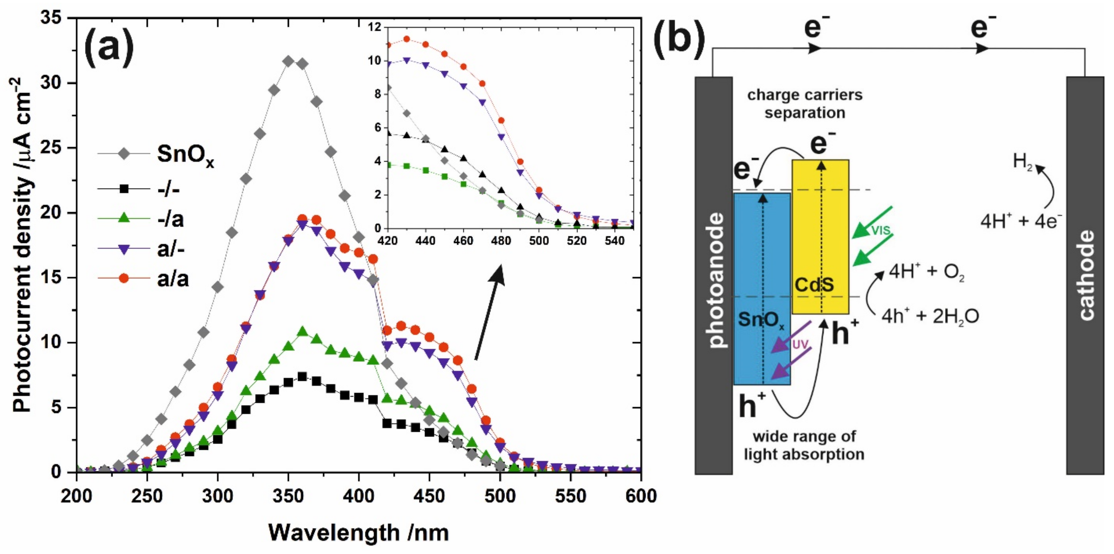
3. Results and Discussion

FE-SEM images of all studied types of nanoporous SnOx/CdS films (see Table 1) are collected in Figure 1. In every case, the porous morphology of the layer is clearly visible, indicating that the SILAR procedure did not cause significant damage to the nanoporous nature of the as-anodized films (compared with the SEM image of the unmodified SnOx layer presented in Figure S1 in Supplementary Information or with those shown in our previous works [14,15]). The only difference is the presence of some brighter areas, suggesting that some other material could be successfully deposited on the surface of SnOx films. Moreover, the edges of channels are less sharp, and some pores seem to be partially filled with other phases (see higher magnification images shown in Figure S2 in Supplementary Information). However, no significant differences in morphological features of all four types of samples can be seen, which indicates an insignificant effect of the thermal treatment on the morphology of the anodic films (as already proved in our previous paper [14]).
EDS spectra of nanoporous SnOx before and after CdS deposition (after annealing) are shown in Figure 2b. Compared to bare SnOx, slight peaks at ca. 2.33 eV and 3.15 eV could be observed in the spectrum recorded for SnOx/CdS, which can be attributed to S and Cd, respectively. Moreover, elemental EDS mapping (see Figure 2c–e) proved a uniform distribution of Sn, Cd, and S on the surface of the anodic film.
XRD patterns of all studied samples did not confirm the presence of the crystalline cadmium sulfide phase even after annealing at 200 °C in air. Figure S3 in Supplementary Information shows the XRD pattern for the a/a sample with no other maxima except those attributed to metallic Sn and SnO phases. It is caused by the overlapping of CdS maxima with those from tin oxides and metallic Sn and, mostly, the low amount of CdS compared to other phases. Therefore, a detailed composition of the surface of nanoporous SnOx/CdS layers was studied by XPS.
The XPS survey spectrum of the a/a sample (see Figure S4 in Supplementary Information) confirmed the presence of Sn, O, Cd, and S on the surface of anodic film after surface modification. The presence of C is the result of typical carbon-containing contaminations adsorbed on the surface during its exposure to the atmosphere. The high-resolution Sn 3d spectrum (Figure 3a) is dominated by two peaks at ca. 487.0 eV and 495.4 eV with a peak separation of 8.4 eV, which can be ascribed to Sn 3d5/2 and Sn 3d3/2, respectively, and correspond to Sn4+-O in SnO2 [29,30,31,32]. Slight peaks at 487.8 eV and 496.2 eV may be attributed to some non-stoichiometric tin oxides or organometallic species originating from the anodic oxidation of the Sn foil. Two sharp peaks at 405.4 eV and 412.1 eV in the Cd 3d spectrum (Figure 3c) with typical splitting energy of 6.7 eV confirm the presence of CdS on the sample surface [33,34,35]. This is in agreement with the S 2p spectrum (Figure 3d), with a characteristic doublet of S 2p3/2 and S 2p1/2 at 161.7 eV and 162.9 eV typically observed for sulfide ions (S2−) [34,35]. The pair of small peaks at ca. 168.7 eV and 170.0 eV suggest the possible presence of some species containing an oxidized form of sulfur (e.g., sulfates) [33], while the peaks at around 163.9 eV and 165.2 eV can be attributed to sulfur or the R-SH groups [33]. However, the ratio of Cd to S was found to be close to 1, independently of the sample type. Moreover, no significant differences in the qualitative surface composition between particular samples have been noticed (positions of all aforementioned peaks varied max by 0.1 eV without any noticeable trend). A detailed inspection of the qualitative surface composition reveals that the amount of oxidized forms of sulfur is higher for the samples subjected to the thermal treatment in the air after deposition of CdS. No other differences between all studied samples were observed.
Optical band gap (Eg) values were estimated from [F(R) hv]2 vs. hv plots (Tauc plots) constructed based on UV-Vis DRS spectra according to the previously described procedure [36] (direct nature of Eg was assumed). As can be seen in Figure 4, the Eg of the samples not subjected to annealing after the SILAR procedure (Figure 4a blue and back lines) are almost the same as those observed for unmodified SnOx (Figure 4b). On the contrary, further annealing of samples modified with CdS results in a noticeable band gap narrowing (Figure 4a—green and red lines) and the narrowest Eg of ca. 2.4 eV is observed for the a/a sample. The value is in excellent agreement with this observed typically for pure CdS (2.42 eV), indicating that cadmium sulfide was effectively deposited on the surface of the porous SnOx layer.
The photocurrent spectra recorded for all studied nanoporous SnOx/CdS photoanodes as well as annealed unmodified SnOx are collected in Figure 5a. Compared to unmodified and annealed SnOx, all SnOx/CdS samples exhibit much lower photocurrents during illumination with UV light. This may be due to local changes in surface chemistry during further immersion of amorphous SnOx matrix in aqueous solutions of Cd2+ and S2− ions (since the worsening of photoresponse in the UV range is much more significant when unannealed samples were modified with CdS). Moreover, the deposition of a thin layer of cadmium sulfide on the tin oxide matrix results in hindered interaction of the wider band gap semiconductor with the light of higher energy. However, at the same time, a dramatic improvement in photoelectrochemical activity in the visible range is observed for the specimens decorated with CdS (see inset in Figure 5a). The photocurrent edge shifts to ca. 510 nm, which perfectly corresponds to the band gap of CdS (ca. 2.4 eV). As expected, thermal treatment of anodic SnOx films before the SILAR procedure seems to be a key factor responsible for the enhanced photoelectrochemical performance due to increased stability of the tin oxide film (as we proved in our previous work [14]) before its further exposure to an aqueous environment. On the contrary, thermal treatment of the sample after deposition of CdS seems to have only a slight positive effect on the photoactivity of the material in the visible range, which can be attributed to the crystallization of cadmium sulfide. At the same time, no effect of post-annealing on the photocurrent values recorded during illumination with UV light was observed, indicating that the tin oxide matrix was unaffected by its further thermal treatment. The enhanced photoelectrochemical properties of SnOx/CdS result from both the presence of a narrow band gap semiconductor, which allows the generation of charge carriers during illumination with visible light, as well as favorable positions of the conduction and valence band edges (both are more negative for CdS compared to SnOx as shown in Figure 5b) that facilitates charge carriers separation and reduces the recombination probability.

4. Conclusions

In summary, we proved that a thin layer of cadmium sulfide can be successfully deposited on the surface of anodically generated nanoporous tin oxide layers via a simple SILAR method. Moreover, the nanoporous morphology of the as-anodized SnOx film is still maintained after CdS deposition. Such SnOx/CdS photoanodes exhibit significantly enhanced photoelectrochemical activity in the visible range due to the lower band gap of CdS (ca. 2.4 eV) and favorable alignment of the band edges. Further investigations are focused on the optimization of the SILAR process (including the number of cycles, solutions composition, the temperature of the process, etc.) to find the optimal thickness of the cadmium sulfide layer as well as possible modification of nanoporous anodic SnOx with other narrow band gap semiconductors.

Supplementary Materials

The following supporting information can be downloaded at: https://www.mdpi.com/article/10.3390/ma15113848/s1, Figure S1: FE-SEM image of the as-anodized SnOx layer before deposition of CdS. Figure S2: Higher magnification FE-SEM image of as-anodized SnOx (left) and SnOx modified with CdS after thermal treatment (right); Figure S3: XRD pattern of the a/a sample.; Figure S4: XPS survey spectrum of the a/a sample.

Author Contributions

K.G.—conceptualization, methodology, investigation, visualization, writing—original draft, and funding acquisition; D.P.—methodology, investigation; M.P.—methodology and data processing (XPS measurements); G.D.S.—supervision and writing—review and editing; L.Z.—conceptualization, methodology, visualization, writing—review and editing, and supervision. All authors have read and agreed to the published version of the manuscript.

Funding

The research was partially supported by the National Science Centre, Poland (Project No. 2016/23/N/ST5/01579).

Institutional Review Board Statement

Not applicable.

Informed Consent Statement

Not applicable.

Data Availability Statement

Not applicable.

Acknowledgments

The SEM imaging was performed in the Laboratory of Field Emission Scanning Electron Microscopy and Microanalysis at the Institute of Geological Sciences, Jagiellonian University, Poland. The authors would like to acknowledge Nan Zhang and Lifeng Liu (International Iberian Nanotechnology Laboratory in Braga, Portugal) for the preliminary XPS measurements and Marcin Kozieł (Faculty of Chemistry, Jagiellonian University) for the interpretation of XRD measurements.

Conflicts of Interest

The authors declare no conflict of interest. The funders had no role in the design of the study; in the collection, analyses, or interpretation of data; in the writing of the manuscript, or in the decision to publish the results.

References

  1. Abe, R. Recent progress on photocatalytic and photoelectrochemical water splitting under visible light irradiation. J. Photochem. Photobiol. C Photochem. Rev. 2010, 11, 179–209. [Google Scholar] [CrossRef]
  2. Osterloh, F.E. Inorganic nanostructures for photoelectrochemical and photocatalytic water splitting. Chem. Soc. Rev. 2012, 42, 2294–2320. [Google Scholar] [CrossRef] [PubMed]
  3. Eftekhari, A.; Babu, V.J.; Ramakrishna, S. Photoelectrode nanomaterials for photoelectrochemical water splitting. Int. J. Hydrogen Energy 2017, 42, 11078–11109. [Google Scholar] [CrossRef]
  4. Zhao, Y.; Hoivik, N.; Wang, K. Recent advance on engineering titanium dioxide nanotubes for photochemical and photoelectrochemical water splitting. Nano Energy 2016, 30, 728–744. [Google Scholar] [CrossRef]
  5. Sołtys-Mróz, M.; Syrek, K.; Wiercigroch, E.; Małek, K.; Rokosz, K.; Raaen, S.; Sulka, G.D. Enhanced visible light photoelectrochemical water splitting using nanotubular FeOx-TiO2 annealed at different temperatures. J. Power Sources 2021, 507, 230274. [Google Scholar] [CrossRef]
  6. Huang, M.-C.; Wang, T.; Wu, B.-J.; Lin, J.-C.; Wu, C.-C. Anodized ZnO nanostructures for photoelectrochemical water splitting. Appl. Surf. Sci. 2016, 360, 442–450. [Google Scholar] [CrossRef]
  7. Mika, K.; Syrek, K.; Uchacz, T.; Sulka, G.D.; Zaraska, L. Dark nanostructured ZnO films formed by anodic oxidation as photoanodes in photoelectrochemical water splitting. Electrochim. Acta 2022, 414, 140176. [Google Scholar] [CrossRef]
  8. Fernández-Domene, R.; Sánchez-Tovar, R.; Lucas-Granados, B.; Roselló-Márquez, G.; Garcia-Anton, J. A simple method to fabricate high-performance nanostructured WO3 photocatalysts with adjusted morphology in the presence of complexing agents. Mater. Des. 2017, 116, 160–170. [Google Scholar] [CrossRef]
  9. Zych, M.; Syrek, K.; Pisarek, M.; Sulka, G.D. Synthesis and characterization of anodic WO3 layers in situ doped with C, N during anodization. Electrochim. Acta 2022, 411, 140061. [Google Scholar] [CrossRef]
  10. Deng, H.; Huang, M.-C.; Weng, W.-H.; Lin, J.-C. Iron oxide nanotube film formed on carbon steel for photoelectrochemical water splitting: Effect of annealing temperature. Surf. Interface Anal. 2016, 48, 1278–1284. [Google Scholar] [CrossRef]
  11. Syrek, K.; Kemona, S.; Czopor, J.; Zaraska, L.; Sulka, G.D. Photoelectrochemical properties of anodic iron oxide layers. J. Electroanal. Chem. 2022, 909, 116143. [Google Scholar] [CrossRef]
  12. Palacios-Padrós, A.; Altomare, M.; Lee, K.; Díez-Pérez, I.; Sanz, F.; Schmuki, P. Controlled thermal annealing tunes the photoelectrochemical properties of nanochanneled tin-oxide structures. ChemElectroChem 2014, 1, 1133–1137. [Google Scholar] [CrossRef]
  13. Zaraska, L.; Gawlak, K.; Gurgul, M.; Chlebda, D.K.; Socha, R.; Sulka, G.D. Controlled synthesis of nanoporous tin oxide layers with various pore diameters and their photoelectrochemical properties. Electrochim. Acta 2017, 254, 238–245. [Google Scholar] [CrossRef]
  14. Zaraska, L.; Gawlak, K.; Wiercigroch, E.; Malek, K.; Kozieł, M.; Andrzejczuk, M.; Marzec, M.M.; Jarosz, M.; Brzozka, A.; Sulka, G.D. The effect of anodizing potential and annealing conditions on the morphology, composition and photoelectrochemical activity of porous anodic tin oxide films. Electrochim. Acta 2019, 319, 18–30. [Google Scholar] [CrossRef]
  15. Zaraska, L.; Gilek, D.; Gawlak, K.; Jaskuła, M.; Sulka, G.D. Formation of crack-free nanoporous tin oxide layers via simple one-step anodic oxidation in NaOH at low applied voltages. Appl. Surf. Sci. 2016, 390, 31–37. [Google Scholar] [CrossRef]
  16. Gurgul, M.; Gawlak, K.; Syrek, K.; Kozieł, M.; Sulka, G.D.; Zaraska, L. The influence of water-induced crystallization on the photoelectrochemical properties of porous anodic tin oxide films. J. Ind. Eng. Chem. 2020, 90, 159–165. [Google Scholar] [CrossRef]
  17. Gurgul, M.; Kozieł, M.; Zaraska, L. Tuning the photoelectrochemical properties of narrow band gap nanoporous anodic SnOx films by simple soaking in water. Materials 2021, 14, 1777. [Google Scholar] [CrossRef]
  18. Wang, L.; Palacios-Padros, A.; Kirchgeorg, R.; Tighineanu, A.; Schmuki, P. Enhanced photoelectrochemical water splitting efficiency of a hematite–ordered Sb:SnO2 host–guest system. ChemSusChem 2014, 7, 421–424. [Google Scholar] [CrossRef]
  19. Shaikh, S.F.; Mane, R.S.; Joo, O.-S. Spraying distance and titanium chloride surface treatment effects on DSSC performance of electrosprayed SnO2 photoanodes. RSC Adv. 2014, 4, 35919–35927. [Google Scholar] [CrossRef]
  20. Shaikh, S.F.; Mane, R.S.; Joo, O.-S. La2O3-encapsulated SnO2 nanocrystallite-based photoanodes for enhanced DSSCs performance. Dalton Trans. 2015, 44, 3075–3081. [Google Scholar] [CrossRef]
  21. Grätzel, M. Photoelectrochemical cells. Nature 2001, 414, 338–344. [Google Scholar] [CrossRef] [PubMed]
  22. Zhang, Z.; Gao, C.; Wu, Z.; Han, W.; Wang, Y.; Fu, W.; Li, X.; Xie, E. Toward efficient photoelectrochemical water-splitting by using screw-like SnO2 nanostructures as photoanode after being decorated with CdS quantum dots. Nano Energy 2016, 19, 318–327. [Google Scholar] [CrossRef]
  23. Liu, Y.; Zhang, P.; Tian, B.; Zhang, J. Core–shell structural CdS@SnO2 nanorods with excellent visible-light photocatalytic activity for the selective oxidation of benzyl alcohol to benzaldehyde. ACS Appl. Mater. Interfaces 2015, 7, 13849–13858. [Google Scholar] [CrossRef] [PubMed]
  24. Memarian, N.; Rozati, S.M.; Concina, I.; Vomiero, A. Deposition of nanostructured CdS thin films by thermal evaporation method: Effect of substrate temperature. Materials 2017, 10, 773. [Google Scholar] [CrossRef]
  25. Rubio, S.; Plaza, J.L.; Diéguez, E. Influence of CdS deposition technique for CdS/CdTe solar cells applications. J. Cryst. Growth 2014, 401, 550–553. [Google Scholar] [CrossRef]
  26. Zhou, X.; Fu, W.; Yang, H.; Li, Y.; Chen, Y.; Sun, M.; Ma, J.; Yang, L.; Zhao, B.; Tian, L. CdS quantum dots sensitized SnO2 photoelectrode for photoelectrochemical application. Electrochim. Acta 2013, 89, 510–515. [Google Scholar] [CrossRef]
  27. Zhou, X.; Zhang, X.; Li, B.; Li, R.; Gao, L.; Zhang, S.; Zhang, M.; Mu, J.; Zhang, X. CdS/CdSe nanoparticles co-deposited SnO2(TiO2) spherical structure film for photoelectrochemical application. Mater. Lett. 2018, 239, 59–62. [Google Scholar] [CrossRef]
  28. Zaraska, L.; Bobruk, M.; Sulka, G.D. Formation of nanoporous tin oxide layers on different substrates during anodic oxidation in oxalic acid electrolyte. Adv. Condens. Matter Phys. 2015, 2015, 302560. [Google Scholar] [CrossRef] [Green Version]
  29. Barreca, D.; Garon, S.; Tondello, E.; Zanella, P. SnO2 nanocrystalline thin films by XPS. Surf. Sci. Spectra 2000, 7, 81–85. [Google Scholar] [CrossRef]
  30. Kwoka, M.; Ottaviano, L.; Passacantando, M.; Santucci, S.; Czempik, G.; Szuber, J. XPS study of the surface chemistry of L-CVD SnO2 thin films after oxidation. Thin Solid Films 2005, 490, 36–42. [Google Scholar] [CrossRef]
  31. Turishchev, S.; Chuvenkova, O.; Parinova, E.; Koyuda, D.; Chumakov, R.; Presselt, M.; Schleusener, A.; Sivakov, V. XPS investigations of MOCVD tin oxide thin layers on Si nanowires array. Results Phys. 2018, 11, 507–509. [Google Scholar] [CrossRef]
  32. Park, B.-E.; Park, J.; Lee, S.; Lee, S.; Kim, W.-H.; Kim, H. Phase-controlled synthesis of SnOx thin films by atomic layer deposition and post-treatment. Appl. Surf. Sci. 2019, 480, 472–477. [Google Scholar] [CrossRef]
  33. Moulder, J.F.; Stickle, W.F.; Sobol, P.W.; Bomben, K.D. Handbook of X-ray Photoelectron Spectroscopy; Perkin-Elmer: Eden Prairie, MN, USA, 1992. [Google Scholar]
  34. Barreca, D.; Gasparotto, A.; Maragno, C.; Tondello, E. Nanostructured cadmium sulfide thin films by XPS. Surf. Sci. Spectra 2002, 9, 46–53. [Google Scholar] [CrossRef]
  35. Stoev, M.; Katerski, A. XPS and XRD study of photoconductive CdS films obtained by a chemical bath deposition process. J. Mater. Chem. 1996, 6, 377–380. [Google Scholar] [CrossRef]
  36. Zaraska, L.; Gawlak, K.; Gurgul, M.; Gilek, D.; Kozieł, M.; Socha, R.P.; Sulka, G.D. Morphology of nanoporous anodic films formed on tin during anodic oxidation in less commonly used acidic and alkaline electrolytes. Surf. Coat. Technol. 2019, 362, 191–199. [Google Scholar] [CrossRef]
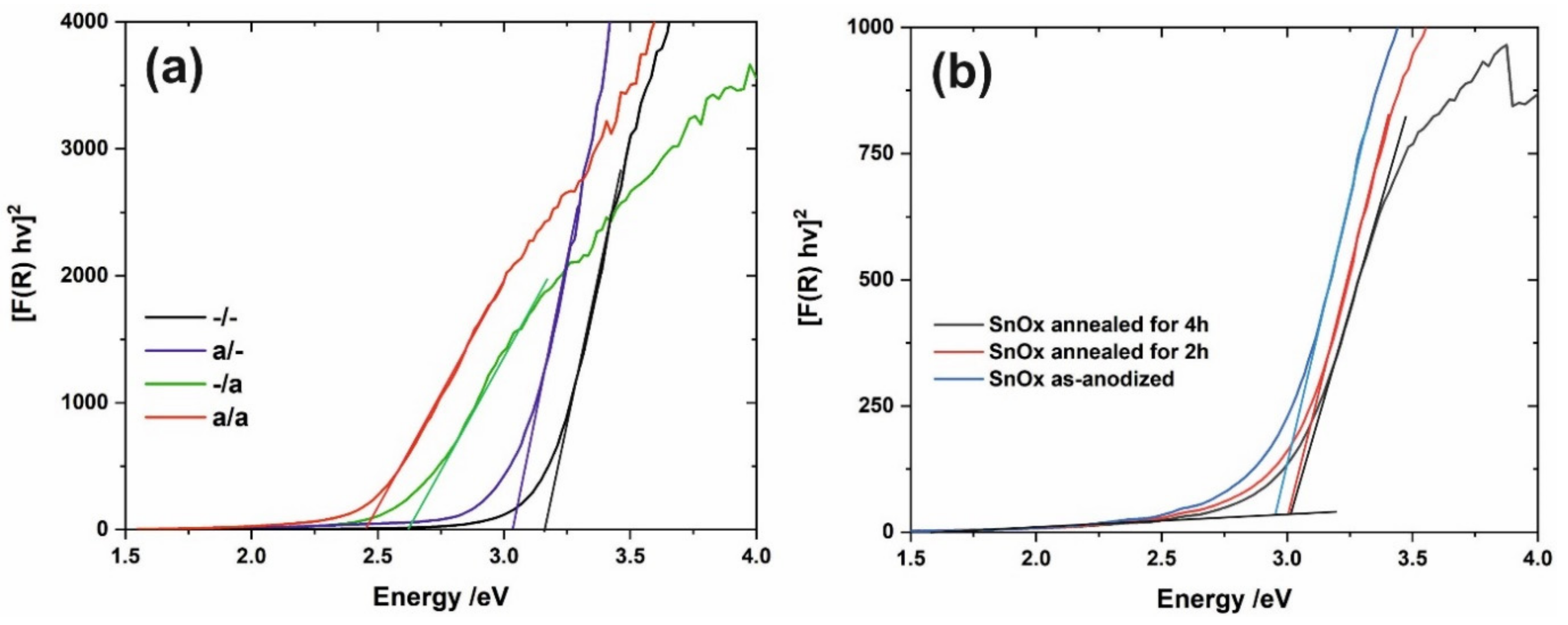
Figure 1. FE-SEM images of different types of SnOx layers after deposition of CdS: -/- (a), -/a (b), a/- (c), and a/a (d).
Materials 15 03848 g001
Figure 2. FE-SEM image of annealed nanoporous SnOx/CdS (a) together with EDS elemental mapping of Sn (c), Cd (d), S (e), and O (f). (b) shows EDS spectra recorded for anodic SnOx (black line) and SnOx/CdS (red line).
Materials 15 03848 g002
Figure 3. High-resolution XPS spectra of Sn 3d (a), O 1s (b), Cd 3d (c), and S 2p (d) recorded for the a/a sample.
Materials 15 03848 g003
Figure 4. [F(R) hv]2 vs. hv plots for all studied nanoporous SnOx/CdS (a) and unmodified porous SnOx (b).
Materials 15 03848 g004
Figure 5. Photocurrent spectra recorded for all studied samples at the potential of 1.0 V vs. SCE in the range between 200 and 550 nm (a), together with a schematic representation of the band alignment and charge transfer between SnOx and CdS (b).
Materials 15 03848 g005
Table 1. Types of SnOx/CdS samples used for detailed studies.
Label of the Sample
-/-a/--/aa/a
Annealing after Anodization
NoYesNoYes
Annealing after SILAR Procedure
NoNoYesYes
Publisher’s Note: MDPI stays neutral with regard to jurisdictional claims in published maps and institutional affiliations.

