Article

Porous Silicon-Zinc Oxide Nanocomposites Prepared by Atomic Layer Deposition for Biophotonic Applications

1
NanoBioMedical Centre, Adam Mickiewicz University, Wszechnicy Piastowskiej 3, 61-614 Poznan, Poland
2
Fondazione Bruno Kessler, Center for Materials and Microsystems IRST, Via Sommarive 18, 38123 Trento, Italy
*
Author to whom correspondence should be addressed.
Materials 2020, 13(8), 1987; https://doi.org/10.3390/ma13081987
Submission received: 27 March 2020 / Revised: 17 April 2020 / Accepted: 22 April 2020 / Published: 24 April 2020
(This article belongs to the Special Issue Multifunctional Nanostructured Silicon Composites)

Abstract

:
In the current research, a porous silicon/zinc oxide (PSi/ZnO) nanocomposite produced by a combination of metal-assisted chemical etching (MACE) and atomic layer deposition (ALD) methods is presented. The applicability of the composite for biophotonics (optical biosensing) was investigated. To characterize the structural and optical properties of the produced PSi/ZnO nanocomposites, several studies were performed: scanning and transmission electron microscopy (SEM/TEM), X-ray diffraction (XRD), X-ray photoelectron spectroscopy (XPS), diffuse reflectance, and photoluminescence (PL). It was found that the ALD ZnO layer fully covers the PSi, and it possesses a polycrystalline wurtzite structure. The effect of the number of ALD cycles and the type of Si doping on the optical properties of nanocomposites was determined. PL measurements showed a “shoulder-shape” emission in the visible range. The mechanisms of the observed PL were discussed. It was demonstrated that the improved PL performance of the PSi/ZnO nanocomposites could be used for implementation in optical biosensor applications. Furthermore, the produced PSi/ZnO nanocomposite was tested for optical/PL biosensing towards mycotoxins (Aflatoxin B1) detection, confirming the applicability of the nanocomposites.

1. Introduction

It is well known that porous silicon (PSi), due to its high surface-to-volume ratio and superior photoluminescence (PL) properties, is an attractive material for optical (bio)sensing applications [1,2]. However, the instability of PSi properties in solutions due to the degradation process needs to be solved in order to obtain a stable response and repeatable results [3]. There are numerous approaches able to reduce the degradation; among them, the deposition of metal oxide onto the PSi is considered to be the most promising one [4,5,6,7,8]. Zinc oxide (ZnO) is one of the possible candidates that could be combined with PSi because of its excellent optical properties (e.g., stable PL signal in the wide optical range), and which may be used in biophotonic applications, particularly biosensors [9,10,11].
Nanocomposites based on PSi/ZnO have attracted more and more attention over the years [12,13,14,15,16]. The underlying reasons behind their popularity are attributed to the synergistic effects on physical and, particularly, optical properties of the PSi/ZnO, which are derived from the combination of individual features of both semiconductors [17,18,19,20,21,22]. The improved catalytic activity, high charge carrier mobility and relatively high biocompatibility make the PSi/ZnO nanocomposite a perfect material for a reliable long-term multipurpose (bio)sensor [23,24,25,26]. Moreover, the outstanding properties of PSi/ZnO nanocomposites related to electroluminescence (EL) [27,28] and photoluminescence (PL) [29,30,31,32] can be tuned through morphology control, such as crystal size, porosity of PSi, and Si to ZnO ratio.
The successive deposition of ZnO on PSi results in the formation of PSi/ZnO nanocomposites, whose properties are strictly affected by the specific deposition method used, such as sol-gel, chemical vapor deposition (CVD), and sputtering methods [33,34,35,36]. These methods have substantial drawbacks related to integration with CMOS technology for commercial sensors production. Moreover, these methods do not allow for the production of a conformal layer of ZnO over the whole surface of PSi or the penetration of ZnO inside the PSi matrix, features that should enhance the active area at the Si-ZnO interface.
One of the most well developed and facile techniques for the deposition of thin metal oxide films on porous materials is atomic layer deposition (ALD) [16,37,38]. This technique allows for the fabrication of highly conformal films of ZnO and other metal oxides over the PSi surface and the production of high-quality nanocomposites in comparison to other methods [4,5,39]. Therefore, ALD is well suited for the synthesis of PSi/ZnO nanocomposites, owing to its precise control of the morphological properties of ZnO. As a consequence, it enables to tune the electronic and optical properties of produced nanocomposites.
A promising approach in the application of PSi/ZnO nanocomposites lies in photonics, particularly in biophotonics. It has been reported that PSi/ZnO nanocomposites demonstrate an intense white light emission that could be used for the development of effective light-emitting diodes [40]. The authors successively achieved a Gaussian-shape emission in the visible range through the tuning of PSi morphology in combination with the ZnO coverage. The influence of oxygen antisites, oxygen vacancies, and quantum confinement effects on the photoluminescence of PSi/ZnO has been discussed in [41], where authors also demonstrated the effect of a SiO2 layer grown between ZnO and PSi on the conductivity of PSi/ZnO nanocomposites. Moreover, the improvement and stabilization of photoluminescence emission have been previously shown in [42], via the passivation of n-type PSi by the deposition of a ZnO layer.
Since ZnO emits light in the visible and UV regions, combining it with PSi leads to the formation of a nanostructure with noticeable white emission [43], which is suitable for sensors application in the visible range. Whereas the PSi/ZnO optical properties can be tuned through morphology parameters, the correlation between PL yield and the structural properties should be thoroughly investigated, especially in the context of sensor applications. D. Gallach-Pérez et al. [41] have reported on the determination of the band diagram of PSi/ZnO nanocomposites by analyzing electroluminescence (EL) spectra and I-V characteristics. It was found that PSi/ZnO broadband emission could be attributed to zinc interstitials (blue emission), oxygen vacancies (green light), and quantum confinement in Si-based quantum dots within PSi, respectively [44,45].
In this paper, we report on the investigation of the structural and optical properties of PSi/ZnO nanocomposites produced from p-type and n-type Si. The ZnO layer was deposited and introduced into the PSi matrix by ALD. The structural properties and chemical composition of the produced nanocomposites were characterized by scanning and transmission electron microscopy (SEM, TEM) combined with an energy dispersive X-Ray spectroscopy (EDX) analysis, an X-Ray diffraction analysis (XRD), and X-Ray photoelectron spectroscopy (XPS). The optical properties of PSi/ZnO nanocomposites were investigated by diffuse reflectance and photoluminescence (PL). The effect of the Si doping-type on the PL properties of PSi/ZnO nanocomposites was analyzed as well. A possible biophotonic application (biosensing towards mycotoxins) is also demonstrated.

2. Materials and Methods

In this study, PSi/ZnO nanocomposites were produced by ALD and metal-assisted chemical etching (MACE). Samples of PSi were produced by MACE on highly doped p-type and n-type Si with (100) orientation and resistivity Ω = 0.01 ohm·cm. As it happens in a typical MACE process, silver nanoparticles were deposited on Si substrates by immersion in the metallization aqueous solution containing 0.2 M HF and 10−3 M AgNO3 for 60 s. The etching process was conducted in an aqueous solution of HF and H2O2 at ratio concentration HF/H2O2/H2O = 80/80/20. Then, the silver nanoparticles were removed by immersion into the HNO3 solution for 60 min.
A commercially available Picosun ALD reactor (Masala, Finland) was used for the deposition of ZnO. The deposition process used diethyl zinc (DEZ) and deionized water as precursors, which reacted at 200 °C and yielded a thickness of 2.1 Å per one ALD cycle (corresponding to a flat surface). The number of ALD cycles was varied as 50, 100, and 250, corresponding to a layer thickness of 10 nm, 20 nm, and 50 nm, respectively. After every cycle, the reactor chamber was purged by an intense N2 flow in order to remove the byproducts of chemical reactions.
The structural properties of PSi/ZnO nanocomposites were analyzed by SEM JEOL JSM 7001F and TEM JEOL ARM 200F (Tokyo, Japan). The XRD measurements were performed by X’pert3 MRD (XL) from PANalytical (Cu Kα radiation source (wavelength of 1.54 Å) and operating at 45 kV and 40 mA (Almelo, The Netherlands).
XPS spectra were recorded with a KRATOS Axis DLD Ultra instrument (Kratos–Manchester, UK) equipped with a hemispherical analyzer and a monochromatic Al Kα (1486.6 eV) X-ray source. The broad spectra (survey) were acquired at 160 eV pass energy, while a higher resolution was used for the acquisition of the core lines, which was performed by setting the pass energy at 20 eV. This allowed to reach an energy resolution of ~0.4 eV. The analyses were acquired at 90° of samples tilted with respect to the analyzer. The spectra were fitted using a freely available software (R-XPS) based on an R-platform (G.Speranza/RxpsG software, RxpsG-2.1 version) [46].
The diffuse reflectance measurements of PSi/ZnO nanocomposites were performed by Ocean Optics QE PRO fiber optic spectrometer (Ostfildern, Germany) combined with an integrating sphere and a Xe light source. Acquisition of PL data was performed at room temperature using a He-Cd laser from Kimmon Koha (Tokyo, Japan) with a wavelength of 325 nm and an output of 5 mW as an excitation source in the range of 400–1000 nm.

3. Results and Discussion

3.1. Structural Properties of PSi/ZnO Nanocomposites
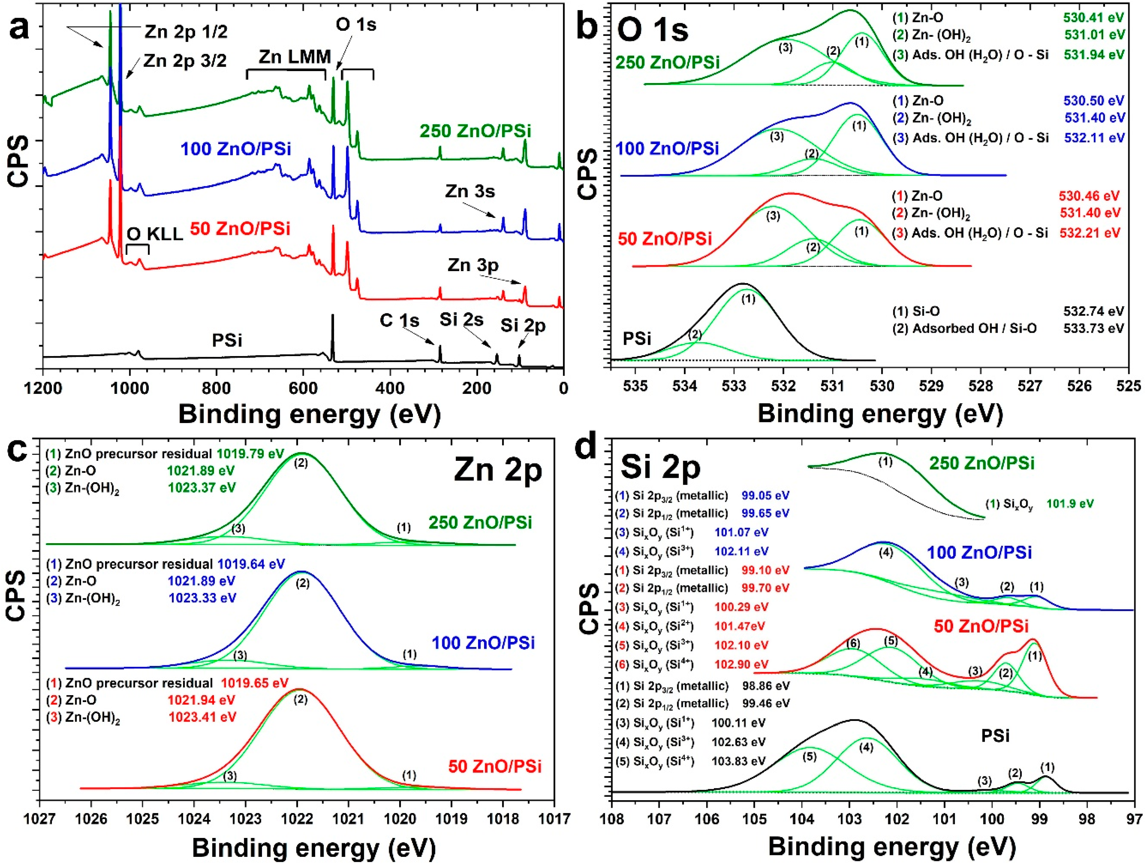
SEM and EDX were performed in order to study the morphology and elemental composition of the produced nanocomposites. The SEM images of PSi and PSi/ZnO nanocomposites derived from p- and n-types Si are represented in Figure 1. Both types of produced PSi samples (Figure 1a,b) show a mesoporous structure (the average size of pores ranged from 10 to 50 nm) with a uniform distribution of the pores. The slightly different roughness of PSi is clearly visible, depending on the type of Si used as a substrate. This might be explained by the different hole concentration during the MACE process, which strongly affects the etching process and as a consequence, defines the surface roughness [47].
After the ALD process, we can observe that the ZnO layer fully covers the PSi (Figure 1c,d). One may also note that the ZnO layer consists of uniformly distributed grains. In addition, the analyses demonstrate that ZnO infiltrates into the PSi matrix. EDX confirms the presence of silicon, oxygen, and zinc atoms after ALD (see Figure 1 insets). EDX mapping indicates the homogeneous distribution of Zn over the whole PSi surface (not shown here).
Figure 2a shows a TEM image of PSi after 100 ALD cycles of ZnO, which correspond to 20 nm of layer thickness. In the TEM image, the presence of ZnO nanocrystallites can be observed. The average size of ZnO nanocrystallites is about 9–11 nm. This result is similar to the value obtained previously for PSi/metal oxide nanocomposites [16,48], once again proving the reproducibility of the method. The Fast Fourier Transform analysis (FFT) shows the highly polycrystalline nature of the deposited ZnO layer, where the wurtzite phase with prevailing (101) and (100) orientations can be indexed.
To determine the structural properties of the PSi/ZnO nanocomposites, XRD measurements were performed. Figure 2c shows the XRD spectra collected from PSi/ZnO with different numbers of ALD cycles: 50, 100, and 250. A clear wurtzite phase pattern can be identified for all samples, represented by (100), (002), (101), (102), (110), and (103) peaks. Some of these peaks are barely detectable for 50 ALD cycles. However, upon increasing the number of ALD cycles, the intensity of wurtzite peaks increases, and the full half maximum (FWHM) is reduced. This confirms the improvement of the ZnO layer crystallinity. Average crystalline sizes were calculated using the Scherrer equation [16,48] and estimated as 6.4 ± 1.5 nm, 7.8 ± 1.2 nm, and 8 ± 1.5 nm for samples deposited with 50, 100, and 250 ALD cycles, respectively. The obtained values corroborate with the experimental data provided by the TEM micrographs.

3.2. XPS Studies

The chemical composition of the produced PSi/ZnO nanocomposites was analyzed by XPS. The survey spectra of PSi and PSi/ZnO samples deposited with different number of ALD cycles are presented in Figure 3a. The surface composition of PSi is primarily dominated by the signals of silicon and oxygen elements. The PSi sample surface displays an abundant contamination of carbon, which originates from the MACE process. All PSi/ZnO samples’ wide spectra are characterized, on the other hand, by the Zn 3p, Zn 3s, O 1s, Zn 2p3/2, and Zn 2p1/2 peaks and the Zn LMM and O KLL Auger peaks. The pattern of survey spectra is generally common for the measured PSi/ZnO samples, but the stoichiometry of the ZnO layer is expected to change with the number of ALD cycles. By considering the XPS high-resolution core lines with their respective experimental sensitivity factors (RSF), the ZnO layer stoichiometry (ratio O/Zn) was determined (Table 1). There is a clear increment of the ZnO stoichiometry with the increase of ALD cycles (the layer thickness). The lower values of the O/Zn for the 50 PSi/ZnO sample could be explained by the high concentration of Zn defects in the deposited layer.
Figure 3b compares the O 1s energy region of the different samples. The O 1s core level peak of as-prepared PSi was deconvoluted into two distinct components at 532.74 eV and 533.73 eV. The first component corresponds to the oxidized PSi surface, while the high-energy component is attributed to absorbed environmental moisture [49]. On the other hand, deconvolution of O 1s peak on samples covered by ZnO shows three components, which are related to Zn-O (530.45 eV) bounds, Zn-(OH)2 (531.40 eV) species, and OH groups (532.1 eV) adsorbed during the ALD process [50]. The intensities and positions of the revealed components of O 1s core line spectra change slightly with the number of ALD cycles. The component responsible for adsorbed water and Si-O bonds is predominant in the 50 ZnO/PSi samples, and noticeably declined in the other samples. This feature can be explained by an increase of ZnO moiety in samples with 100 and 250 cycles and resulted in an increment in Zn-O components.
The detailed spectra of Zn 2p core levels are presented in Figure 3c. The Zn 2p3/2 peak was fitted with two main components located at 1021.89 eV and 1023.37 eV (corresponding to Zn-O and Zn-(OH)2) and an extremely weak third component at 1019.79 eV, which may be attributed to some residuals of unreacted Zn precursor [50]. Attribution of the component at 1023.37 eV to hydroxide species is corroborated by the O 1s peak at 531.4 eV. The presence of metal oxide-OH species on the surface has been previously observed for ZnO as well as for TiO2, Al2O3, and RuO2 produced by ALD [5,39,49,50]. One may conclude that this is a feature of produced ALD metal oxides.
No signal from Si is clearly visible from the survey of PSi/ZnO nanocomposites. Its presence was checked by acquiring a detailed spectrum in the region of Si 2p core line, in order to verify if a small signal coming from the surface oxide was still visible, even after the deposition of 250 cycles of ZnO. In the Si 2p core line (Figure 3d), it is clearly visible in the metallic component with the spin-orbit doublet, which can be easily resolved into its 2p1/2 and 2p3/2 contributions. The silicon oxide layer generates a broad peak at higher binding energies, which can be resolved by overlapping at least 3 components, due to the different possible oxidation states of Si (Si1+, Si2+, Si3+ or Si4+). A more visible signal coming from the silicon substrate can be detected by decreasing the number of ALD cycles, and both the metallic doublet and the oxide components can be distinguished.

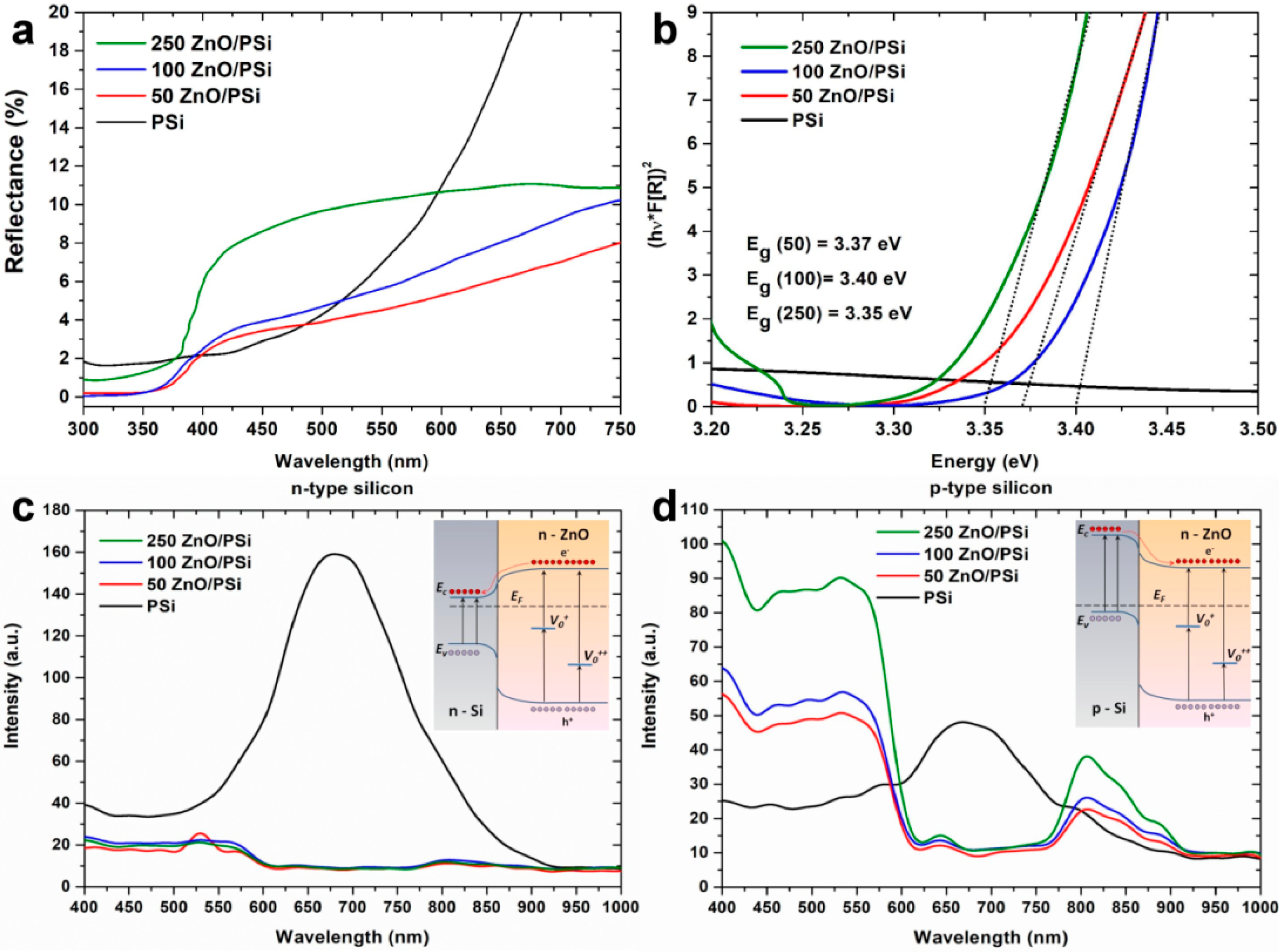
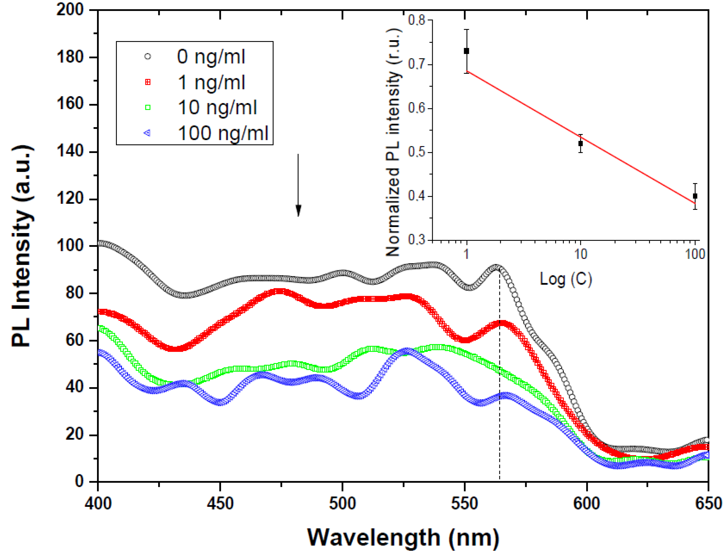
3.3. Optical and Biosensing Properties

In order to elucidate the optical properties of the produced PSi/ZnO nanocomposites, the diffuse reflectance and the photoluminescence were measured in the ranges of 300–750 nm and 400–1000 nm, respectively.
Diffuse reflectance spectra for as-prepared PSi and PSi/ZnO with 50, 100, and 250 ALD cycles are shown in Figure 4a. All the samples show a significantly low reflectance in the UV region, and a noticeable increase in the visible region up to 10% for 250 cycles of ZnO. Recalculation of the obtained data into a representation of a Tauc plot was performed according to the Kubelka-Munk theory via F(R) function: F ( R ) = ( 1 R ) 2 2 R = k S [5], where R is the absolute reflectance of the PSi/ZnO sample, k is the absorption coefficient, and s is the scattering coefficient (Figure 4b). The calculated band gap (Eg) values are 3.37 eV, 3.40 eV, and 3.35 eV for samples with 50, 100, and 250 ALD cycles, respectively. Such values are close to the bulk ZnO Eg value, thus proving the good crystallinity of the produced ALD layers.
PL measurements were conducted to investigate the recombination processes in the Si-ZnO interface. PL spectra were measured for PSi/ZnO nanocomposites produced from n- and p-type of Si (Figure 4c,d). The as-prepared PSi demonstrates a strong red PL emission at approximately 670 nm (1.85 eV) for both types of Si. It is well known that the visible emission of PSi is attributed to the quantum confinement effect of Si nanocrystallites, which are formed during etching processes [51,52]. After the ZnO deposition, the PL spectrum changes depending on the type of initial Si. Figure 4c demonstrates the PL quenching for n-type PSi/ZnO nanocomposites. However, one may observe significant PL changes for p-type PSi/ZnO nanocomposites (Figure 4d). The p-type PSi/ZnO nanocomposites demonstrate an intensive white PL emission with a strong “shoulder-shape” contribution in the 400–600 nm region, and a weak Infra-red (IR) emission in the 800–900 nm region. The “shoulder-shape” PL in the visible range probably originates from the complex mechanism of the recombination emission through defect levels of ZnO, which may be attributed to radiative recombination at single and double-charged oxygen vacancy (Vo+, Vo++) sites [35,53]. However, the full interpretation and explanation of observed PL will be the aim of future research.
One could propose a simpler explanation of the observed experimental results based on the analysis of energy band diagrams for the Si-ZnO interface (insets in Figure 4c,d). It is well known that oxygen vacancies (depicted as Vo+, Vo++ in the energy band diagrams) are the most widely accepted mechanisms of the visible emission in ZnO. Let us assume that all laser radiation is adsorbed in the top ZnO layer. In the case of n-type PSi/ZnO, according to the energy band diagrams, it can be seen that the electrons and holes photogenerated in the ZnO layer should be drifted to the Si. These photogenerated charge carriers are recombined through non-radiative surface defects, probably associated with SiOx, the presence of which was confirmed by XPS. In the case of p-type PSi/ZnO, the interface of p- and n-type semiconductors induces the formation of a potential barrier for photogenerated electrons in ZnO (see inset Figure 4d). Thus, photogenerated charge carriers tend to recombine through defect levels of ZnO. An increased intensity of PL around the 400 nm edge probably originates from the exciton recombination in ZnO [16]. The presence of red/IR PL may be explained by additional defect states on the surface of n-PSi/ZnO nanocomposite [34,54].
The PL analysis demonstrates that p-type PSi/ZnO nanocomposites are more favorable for the development of novel biophotonic (e.g., optical biosensors) devices. This nanocomposite was tested for optical/PL biosensing applications towards mycotoxins (Aflatoxin B1) detection. We analyzed the evaluation of the PL spectrum, depending on the concentration of AFB1 probed on the surface. The formation of the bioselective layer for AFB1 was performed according to the protocol based on previous works [55,56]. Briefly, the PSi/ZnO was treated with 4% APTES in Ethanol with the following carboxyl groups activation in a solution of 2% glutaraldehyde in distilled water. In the next step, 50 μg/mL of Anti-AFB1 (in PBS) was added to achieve a selective layer to AFB1. Before the experiment, the samples were washed with PBS and gently dried using an N2 flow. Then, the probe of the PBS/AFB1 solution (1, 10, and 100 ng/mL) was dropped onto the surface of the PSi/ZnO nanocomposite and washed with PBS after 20 min.
Figure 5 represents the PL response of PSi/ZnO nanocomposite in comparison to different concentrations of AFB1. The PL-based detection of AFB1 on the PSi/ZnO nanostructure shows sequential PL (λ = 565 nm) quenching from the lower to the highest AFB1 concentration, which makes the PSi/ZnO nanocomposite a suitable material for further usage in real-time (bio)molecule detection. Furthermore, the inset in Figure 5 indicates a good linearity of sensor response, which is the key parameter for the development of effective biosensors [57]. Thus, based on the evidence mentioned above, PSi/ZnO could be used as a significant potential optical biosensing platform for different types of biomolecules.

4. Conclusions

In summary, PSi/ZnO nanocomposites were fabricated using MACE and ALD techniques. Their structural properties and chemical compositions were determined. The approximate size of ZnO nanograins was estimated using XRD and TEM analysis. The effect of the number of ALD cycles and the type of Si used as substrate on the optical properties of nanocomposites were studied. Optical properties (reflectance and band gap energy) of PSi/ZnO nanocomposites were tailored by their structural parameters. It was demonstrated that an effective white “shoulder-shape” may be used for implantation in optical biosensor applications toward mycotoxins (Aflatoxin B1) detection, as a model molecule.

Author Contributions

Conceptualization and conception, I.I.; methodology, I.I.; sample fabrication, M.P., M.J., and I.I.; XRD, SEM investigations, E.C.; XPS investigations, G.G.; optical investigations, M.P.and I.I.; biosensing tests, V.M. and I.I.; interpretation of data, M.P., V.M., G.G. and I.I.; writing—original draft preparation, M.P, V.M. and I.I.; writing—review and editing, I.I.; drafting the work, I.I.; supervision, I.I.; project administration, I.I.; funding acquisition, I.I. All authors have read and agreed to the published version of the manuscript.

Funding

This research was funded by SONATA 11 project UMO-2016/21/D/ST3/00962 from the National Science Centre of Poland.

Acknowledgments

Authors acknowledge the support from Stefan Jurga (CNBM-AMU). M.P. and V.M. acknowledge the partial financial support from the project “Środowiskowe interdyscyplinarne studia doktoranckie w zakresie nanotechnologii” No. POWR.03.02.00-00-I032/16 under the European Social Fund–Operational Programme Knowledge Education Development, Axis III Higher Education for Economy and Development, Action 3.2 PhD Programme. I.I., E.C. and G.G. acknowledge the partial financial support by project H2020-MSCA-RISE-2017, ‘Novel 1D photonic metal oxide nanostructures for early stage cancer detection’ (Project number: 778157).

Conflicts of Interest

The authors declare no conflict of interest.

References

  1. Myndrul, V.; Iatsunskyi, I. Nanosilicon-Based Composites for (Bio)sensing Applications: Current Status, Advantages, and Perspectives. Materials 2019, 12, 2880. [Google Scholar] [CrossRef] [Green Version]
  2. Iatsunskyi, I.; Smyntyna, V.; Pavlenko, M.; Kanevska, O.; Kirik, Y.; Myndrul, V. Ammonia detection using optical reflectance from porous silicon formed by metal-assisted chemical etching. In Proceedings of the Optics and Photonics for Counterterrorism, Crime Fighting and Defence IX; and Optical Materials and Biomaterials in Security and Defence Systems Technology X, Dresden, Germany, 23–24 September 2013; p. 8901. [Google Scholar]
  3. Tischler, M.A.; Collins, R.T.; Stathis, J.H.; Tsang, J.C. Luminescence degradation in porous silicon. Appl. Phys. Lett. 1992, 60, 639–641. [Google Scholar] [CrossRef]
  4. Iatsunskyi, I.; Jancelewicz, M.; Nowaczyk, G.; Kempiński, M.; Peplińska, B.; Jarek, M.; Załęski, K.; Jurga, S.; Smyntyna, V. Atomic layer deposition TiO2 coated porous silicon surface: Structural characterization and morphological features. Thin Solid Films 2015, 589, 303–308. [Google Scholar] [CrossRef]
  5. Brytavskyi, I.; Hušeková, K.; Myndrul, V.; Pavlenko, M.; Coy, E.; Zaleski, K.; Gregušová, D.; Yate, L.; Smyntyna, V.; Iatsunskyi, I. Effect of porous silicon substrate on structural, mechanical and optical properties of MOCVD and ALD ruthenium oxide nanolayers. Appl. Surf. Sci. 2019, 471, 686–693. [Google Scholar] [CrossRef]
  6. Silina, Y.E.; Koch, M.; Herbeck-Engel, P.; Iatsunskyi, I. Exploring the potential of high resolution inductively coupled plasma mass spectrometry towards non-destructive control and validation of electroless gold nanoparticles onto silicon nanowires hybrids. Anal. Methods 2019, 11, 3987–3995. [Google Scholar] [CrossRef]
  7. Pavlenko, M.; Siuzdak, K.; Coy, E.; Jancelewicz, M.; Jurga, S.; Iatsunskyi, I. Silicon/TiO2 core-shell nanopillar photoanodes for enhanced photoelectrochemical water oxidation. Int. J. Hydrogen Energy 2017, 42, 30076–30085. [Google Scholar] [CrossRef]
  8. Pavlenko, M.; Coy, E.L.; Jancelewicz, M.; Załȩski, K.; Smyntyna, V.; Jurga, S.; Iatsunskyi, I.; Zaleski, K.; Smyntyna, V.; Jurga, S.; et al. Enhancement of optical and mechanical properties of Si nanopillars by ALD TiO2 coating. RSC Adv. 2016, 6, 97070–97076. [Google Scholar] [CrossRef]
  9. Viter, R.; Savchuk, M.; Iatsunskyi, I.; Pietralik, Z.; Starodub, N.; Shpyrka, N.; Ramanaviciene, A.; Ramanavicius, A. Analytical, thermodynamical and kinetic characteristics of photoluminescence immunosensor for the determination of Ochratoxin A. Biosens. Bioelectron. 2018, 99, 237–243. [Google Scholar] [CrossRef]
  10. Tamashevski, A.; Harmaza, Y.; Viter, R.; Jevdokimovs, D.; Poplausks, R.; Slobozhanina, E.; Mikoliunaite, L.; Erts, D.; Ramanaviciene, A.; Ramanavicius, A. Zinc oxide nanorod based immunosensing platform for the determination of human leukemic cells. Talanta 2019, 200, 378–386. [Google Scholar] [CrossRef] [Green Version]
  11. Viter, R.; Savchuk, M.; Starodub, N.; Balevicius, Z.; Tumenas, S.; Ramanaviciene, A.; Jevdokimovs, D.; Erts, D.; Iatsunskyi, I.; Ramanavicius, A. Photoluminescence immunosensor based on bovine leukemia virus proteins immobilized on the ZnO nanorods. Sens. Actuators B Chem. 2019, 285, 601–606. [Google Scholar] [CrossRef] [Green Version]
  12. Rusli, N.I.; Tanikawa, M.; Mahmood, M.R.; Yasui, K.; Hashim, A.M. Growth of high-density zinc oxide nanorods on porous silicon by thermal evaporation. Materials 2012, 5, 2817–2832. [Google Scholar] [CrossRef] [Green Version]
  13. Hsu, H.-C.; Cheng, C.-S.; Chang, C.-C.; Yang, S.; Chang, C.-S.; Hsieh, W.-F. Orientation-enhanced growth and optical properties of ZnO nanowires grown on porous silicon substrates. Nanotechnology 2005, 16, 297–301. [Google Scholar] [CrossRef]
  14. Kanungo, J.; Saha, H.; Basu, S. Pd sensitized porous silicon hydrogen sensor—Influence of ZnO thin film. Sens. Actuators B Chem. 2010, 147, 128–136. [Google Scholar] [CrossRef]
  15. Yan, D.; Hu, M.; Li, S.; Liang, J.; Wu, Y.; Ma, S. Electrochemical deposition of ZnO nanostructures onto porous silicon and their enhanced gas sensing to NO2 at room temperature. Electrochim. Acta 2014, 115, 297–305. [Google Scholar] [CrossRef]
  16. Graniel, O.; Fedorenko, V.; Viter, R.; Iatsunskyi, I.; Nowaczyk, G.; Weber, M.; Załęski, K.; Jurga, S.; Smyntyna, V.; Miele, P.; et al. Optical properties of ZnO deposited by atomic layer deposition (ALD) on Si nanowires. Mater. Sci. Eng. B 2018, 236–237, 139–146. [Google Scholar] [CrossRef] [Green Version]
  17. Wang, Z.; Yu, R.; Wang, X.; Wu, W.; Wang, Z.L. Ultrafast Response p-Si/n-ZnO Heterojunction Ultraviolet Detector Based on Pyro-Phototronic Effect. Adv. Mater. 2016, 28, 6880–6886. [Google Scholar] [CrossRef]
  18. Huang, C.-Y.; Yang, Y.-J.; Chen, J.-Y.; Wang, C.-H.; Chen, Y.-F.; Hong, L.-S.; Liu, C.-S.; Wu, C.-Y. p-Si nanowires/SiO2/n-ZnO heterojunction photodiodes. Appl. Phys. Lett. 2010, 97, 013503. [Google Scholar] [CrossRef]
  19. Guo, Z.; Zhao, D.; Liu, Y.; Shen, D.; Zhang, J.; Li, B. Visible and ultraviolet light alternative photodetector based on ZnO nanowire/n-Si heterojunction. Appl. Phys. Lett. 2008, 93, 163501. [Google Scholar] [CrossRef] [Green Version]
  20. Choi, J.-H.; Das, S.N.; Moon, K.-J.; Kar, J.P.; Myoung, J.-M. Fabrication and characterization of p-Si nanowires/ZnO film heterojunction diode. Solid State Electron. 2010, 54, 1582–1585. [Google Scholar] [CrossRef]
  21. Zhang, H.; Jia, Z. Application of porous silicon microcavity to enhance photoluminescence of ZnO/PS nanocomposites in UV light emission. Optik (Stuttg) 2017, 130, 1183–1190. [Google Scholar] [CrossRef] [Green Version]
  22. Shabnam; Kant, C.R.; Arun, P. White-light emission from annealed ZnO:Si nanocomposite thin films. J. Lumin. 2012, 132, 1744–1749. [Google Scholar] [CrossRef] [Green Version]
  23. Shanmugam, N.R.; Muthukumar, S.; Prasad, S. A review on ZnO-based electrical biosensors for cardiac biomarker detection. Future Sci. OA 2017, 3, FSO196. [Google Scholar] [CrossRef] [PubMed] [Green Version]
  24. Tripathy, N.; Kim, D.-H. Metal oxide modified ZnO nanomaterials for biosensor applications. Nano Converg. 2018, 5, 27. [Google Scholar] [CrossRef] [PubMed]
  25. Napi, M.L.M.; Sultan, S.M.; Ismail, R.; How, K.W.; Ahmad, M.K. Electrochemical-Based Biosensors on Different Zinc Oxide Nanostructures: A Review. Materials 2019, 12, 2985. [Google Scholar] [CrossRef] [Green Version]
  26. Sampath, S.; Shestakova, M.; Maydannik, P.; Ivanova, T.; Homola, T.; Bryukvin, A.; Sillanpää, M.; Nagumothu, R.; Alagan, V. Photoelectrocatalytic activity of ZnO coated nano-porous silicon by atomic layer deposition. RSC Adv. 2016, 6, 25173–25178. [Google Scholar] [CrossRef] [Green Version]
  27. Sun, H.; Zhang, Q.-F.; Wu, J.-L. Electroluminescence from ZnO nanorods with an n-ZnO/p-Si heterojunction structure. Nanotechnology 2006, 17, 2271–2274. [Google Scholar] [CrossRef]
  28. Ye, J.D.; Gu, S.L.; Zhu, S.M.; Liu, W.; Liu, S.M.; Zhang, R.; Shi, Y.; Zheng, Y.D. Electroluminescent and transport mechanisms of n-ZnO/p-Si heterojunctions. Appl. Phys. Lett. 2006, 88, 182112. [Google Scholar] [CrossRef]
  29. Palanivelu, R.; Rubankumar, A. Synthesis and Spectroscopic Characterization of Hydroxyapatite by Sol-Gel Method. Int. J. ChemTech Res. 2013, 5, 2965–2969. [Google Scholar]
  30. Singh, R.G.; Singh, F.; Agarwal, V.; Mehra, R.M. Photoluminescence studies of ZnO/porous silicon nanocomposites. J. Phys. D Appl. Phys. 2007, 40, 3090–3093. [Google Scholar] [CrossRef]
  31. Ambrosio, R.; Galindo, F.; Morales–Morales, F.; Moreno, M.; Torres, A.; Vásquez-A, M.A.; Pérez García, S.A.; Morales–Sánchez, A. Effect of the thermal annealing on the structural, morphological and photoluminescent properties of ZnO/Si multilayers. Opt. Mater. 2019, 96, 109339. [Google Scholar] [CrossRef]
  32. Olenych, I.B.; Monastyrskii, L.S.; Luchechko, A.P. Photoluminescence of Porous Silicon–Zinc Oxide Hybrid structures. J. Appl. Spectrosc. 2017, 84, 66–70. [Google Scholar] [CrossRef]
  33. Sun, L.; He, H.; Liu, C.; Lu, Y.; Ye, Z. Controllable growth and optical properties of ZnO nanostructures on Si nanowire arrays. CrystEngComm 2011, 13, 2439–2444. [Google Scholar] [CrossRef]
  34. Dalvand, R.; Mahmud, S.; Alimanesh, M.; Vakili, A.H. Optical and structural properties of well-aligned ZnO nanoneedle arrays grown on porous silicon substrates by electric field-assisted aqueous solution method. Ceram. Int. 2017, 43, 1488–1494. [Google Scholar] [CrossRef]
  35. Singh, R.G.; Singh, F.; Kanjilal, D.; Agarwal, V.; Mehra, R.M. White light emission from chemically synthesized ZnO–porous silicon nanocomposite. J. Phys. D Appl. Phys. 2009, 42, 062002. [Google Scholar] [CrossRef]
  36. Graniel, O.; Iatsunskyi, I.; Coy, E.; Humbert, C.; Barbillon, G.; Michel, T.; Maurin, D.; Balme, S.; Miele, P.; Bechelany, M. Au-covered hollow urchin-like ZnO nanostructures for surface-enhanced Raman scattering sensing. J. Mater. Chem. C 2019, 7, 15066–15073. [Google Scholar] [CrossRef]
  37. Iatsunskyi, I.; Baitimirova, M.; Coy, E.; Yate, L.; Viter, R.; Ramanavicius, A.; Jurga, S.; Bechelany, M.; Erts, D. Influence of ZnO/graphene nanolaminate periodicity on their structural and mechanical properties. J. Mater. Sci. Technol. 2018, 34, 1487–1493. [Google Scholar] [CrossRef]
  38. Titov, V.V.; Lisachenko, A.A.; Akopyan, I.K.; Labzowskaya, M.E.; Novikov, B.V. On the nature of the effect of adsorbed oxygen on the excitonic photoluminescence of ZnO. J. Lumin. 2018, 195, 153–158. [Google Scholar] [CrossRef]
  39. Iatsunskyi, I.; Kempiński, M.; Jancelewicz, M.; Załęski, K.; Jurga, S.; Smyntyna, V. Structural and XPS characterization of ALD Al2O3 coated porous silicon. Vacuum 2015, 113, 52–58. [Google Scholar] [CrossRef]
  40. Dellis, S.; Pliatsikas, N.; Kalfagiannis, N.; Lidor-Shalev, O.; Papaderakis, A.; Vourlias, G.; Sotiropoulos, S.; Koutsogeorgis, D.C.; Mastai, Y.; Patsalas, P. Broadband luminescence in defect-engineered electrochemically produced porous Si/ZnO nanostructures. Sci. Rep. 2018, 8, 6988. [Google Scholar] [CrossRef]
  41. Gallach-Pérez, D.; Muñoz-Noval, A.; García-Pelayo, L.; Manso-Silván, M.; Torres-Costa, V. Tunnel conduction regimes, white-light emission and band diagram of porous silicon–zinc oxide nanocomposites. J. Lumin. 2017, 191, 107–111. [Google Scholar] [CrossRef]
  42. Prabakaran, R.; Peres, M.; Monteiro, T.; Fortunato, E.; Martins, R.; Ferreira, I. The effects of ZnO coating on the photoluminescence properties of porous silicon for the advanced optoelectronic devices. J. Non-Cryst. Solids 2008, 354, 2181–2185. [Google Scholar] [CrossRef]
  43. Kayahan, E. White light luminescence from annealed thin ZnO deposited porous silicon. J. Lumin. 2010, 130, 1295–1299. [Google Scholar] [CrossRef]
  44. Algün, G.; Akçay, N. The role of etching current density and porous structure on enhanced photovoltaic performance of ZnO/PS heterojunction solar cells. Appl. Phys. A 2019, 125, 568. [Google Scholar] [CrossRef]
  45. Aydemir, G.; Utlu, G.; Çetinel, A. Growth and characterization of ZnO nanostructures on porous silicon substrates: Effect of solution temperature. Chem. Phys. Lett. 2019, 737, 136827. [Google Scholar] [CrossRef]
  46. Speranza, G.; Canteri, R. RxpsG a new open project for Photoelectron and Electron Spectroscopy data processing. SoftwareX 2019, 10, 100282. [Google Scholar] [CrossRef]
  47. Han, H.; Huang, Z.; Lee, W. Metal-assisted chemical etching of silicon and nanotechnology applications. Nano Today 2014, 9, 271–304. [Google Scholar] [CrossRef] [Green Version]
  48. Iatsunskyi, I.; Pavlenko, M.; Viter, R.; Jancelewicz, M.; Nowaczyk, G.; Baleviciute, I.; Załęski, K.; Jurga, S.; Ramanavicius, A.; Smyntyna, V. Tailoring the Structural, Optical, and Photoluminescence Properties of Porous Silicon/TiO2 Nanostructures. J. Phys. Chem. C 2015, 119, 7164–7171. [Google Scholar] [CrossRef]
  49. Iatsunskyi, I.; Kempiński, M.; Nowaczyk, G.; Jancelewicz, M.; Pavlenko, M.; Załęski, K.; Jurga, S. Structural and XPS studies of PSi/TiO2 nanocomposites prepared by ALD and Ag-assisted chemical etching. Appl. Surf. Sci. 2015, 347, 777–783. [Google Scholar] [CrossRef]
  50. Iatsunskyi, I.; Vasylenko, A.; Viter, R.; Kempiński, M.; Nowaczyk, G.; Jurga, S.; Bechelany, M. Tailoring of the electronic properties of ZnO-polyacrylonitrile nanofibers: Experiment and theory. Appl. Surf. Sci. 2017, 411, 494–501. [Google Scholar] [CrossRef]
  51. Bisi, O.; Ossicini, S.; Pavesi, L. Porous silicon: A quantum sponge structure for silicon based optoelectronics. Surf. Sci. Rep. 2000, 38, 1–126. [Google Scholar] [CrossRef]
  52. Iatsunskyi, I.; Nowaczyk, G.; Jurga, S.; Fedorenko, V.; Pavlenko, M.; Smyntyna, V. One and two-phonon Raman scattering from nanostructured silicon. Optik 2015, 126, 1650–1655. [Google Scholar] [CrossRef] [Green Version]
  53. Marin, O.; Grinblat, G.; María, A.; Tirado, M.; Koropecki, R.R.; Comedi, D. Superlattices and Microstructures On the origin of white photoluminescence from ZnO nanocones/porous silicon heterostructures at room temperature. Superlattices Microstruct. 2015, 79, 29–37. [Google Scholar] [CrossRef]
  54. Ma, Q.L.; Zhai, B.G.; Huang, Y.M. Sol-gel derived ZnO/porous silicon composites for tunable photoluminescence. J. Sol-Gel Sci. Technol. 2012, 64, 110–116. [Google Scholar] [CrossRef]
  55. Iatsunskyi, I.; Myndrul, V.; Smyntyna, V.; Viter, R.; Melnyk, Y.; Pavlova, K. Porous silicon photoluminescence biosensor for rapid and sensitive detection of toxins. Org. Sens. Bioelectron. X 2017, 10364, 28. [Google Scholar] [CrossRef]
  56. Myndrul, V.; Viter, R.; Savchuk, M.; Koval, M.; Starodub, N.; Silamiķelis, V.; Smyntyna, V.; Ramanavicius, A.; Iatsunskyi, I. Gold coated porous silicon nanocomposite as a substrate for photoluminescence-based immunosensor suitable for the determination of Aflatoxin B1. Talanta 2017, 175, 297–304. [Google Scholar] [CrossRef]
  57. Viter, R.; Iatsunskyi, I. Metal Oxide Nanostructures in Sensing. In Nanomaterials Design for Sensing Applications; Zenkina, O.V., Ed.; Elsevier: Amsterdam, The Netherlands, 2019; pp. 41–91. ISBN 978-0-12-814505-0. [Google Scholar]
Figure 1. SEM images of porous silicon (PSi) surface before and after 100 cycles of zinc oxide ALD: (a) n-type PSi; (b) p-type PSi; (c,d) n-and p-types PSi after zinc oxide (ZnO) deposition, respectively (insets: an EDX analysis).
Materials 13 01987 g001
Figure 2. (a) TEM imaging of ZnO nanocrystallites on PSi obtained after 100 ALD cycles; (b) FFT of the PSi/ZnO TEM image; (c) GIXRD spectra of PSi/ZnO nanocomposites with 250, 100, and 50 ALD cycles of ZnO in comparison to GIXRD spectrum of PSi. Standard diffraction peaks of wurtzite (pdf card #36-1451) are presented for reference.
Materials 13 01987 g002
Figure 3. XPS survey and core-level spectra of PSi/ZnO with 50, 100, and 250 ALD cycles: (a) total survey spectra; (bd) O 1s, Zn 2p, Si 2p energy regions, respectively. Corresponding binding energy values obtained by the deconvolution of the detected peaks are shown in the insets.
Materials 13 01987 g003
Figure 4. Optical properties of the fabricated PSi/ZnO nanocomposites: (a) diffuse reflectance spectra of PSi/ZnO nanocomposites; (b) absorption edges and corresponding energy band gap values; photoluminescence spectra for (c) n-PSi/ZnO and (d) p-PSi/ZnO nanocomposites. The energy band diagrams of corresponding excitation mechanisms are depicted in the insets.
Materials 13 01987 g004
Figure 5. PL response of p-type PSi/ZnO toward different AFB1 concentrations. The inset graph indicates the linearity of PL response to three different concentrations of AFB1 in a half-logarithmic scale with an error bar.
Materials 13 01987 g005
Table 1. ZnO layer stoichiometry.
SampleZn (in Zn-O), at. %O (in Zn-O), at %O/Zn
250 PSi/ZnO17.8518.211.02
100 PSi/ZnO20.5420.380.99
50 PSi/ZnO15.4814.000.90

