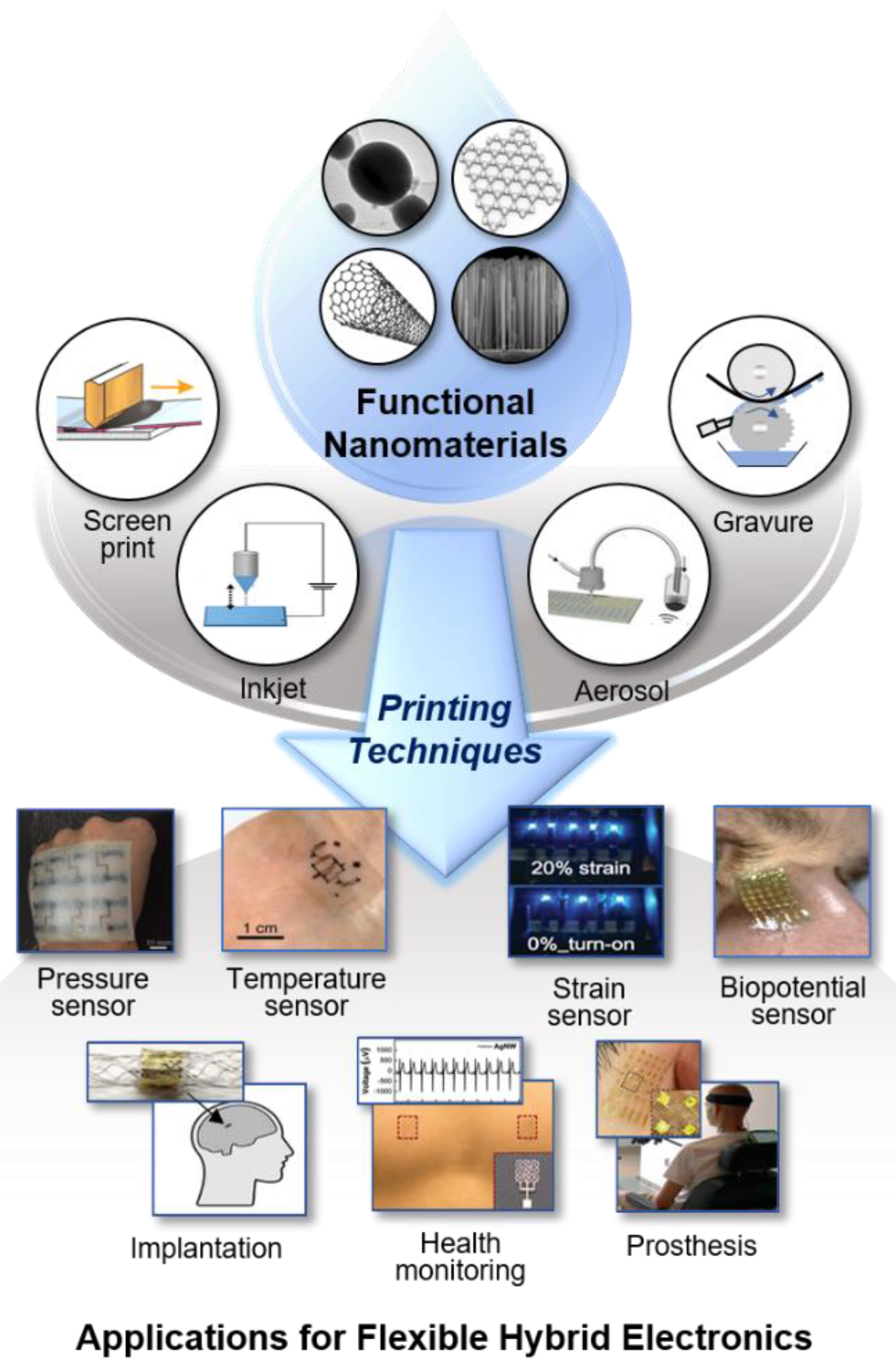
Advanced Nanomaterials, Printing Processes, and Applications for Flexible Hybrid Electronics


Abstract
1. Introduction
2. Printable Nanomaterials
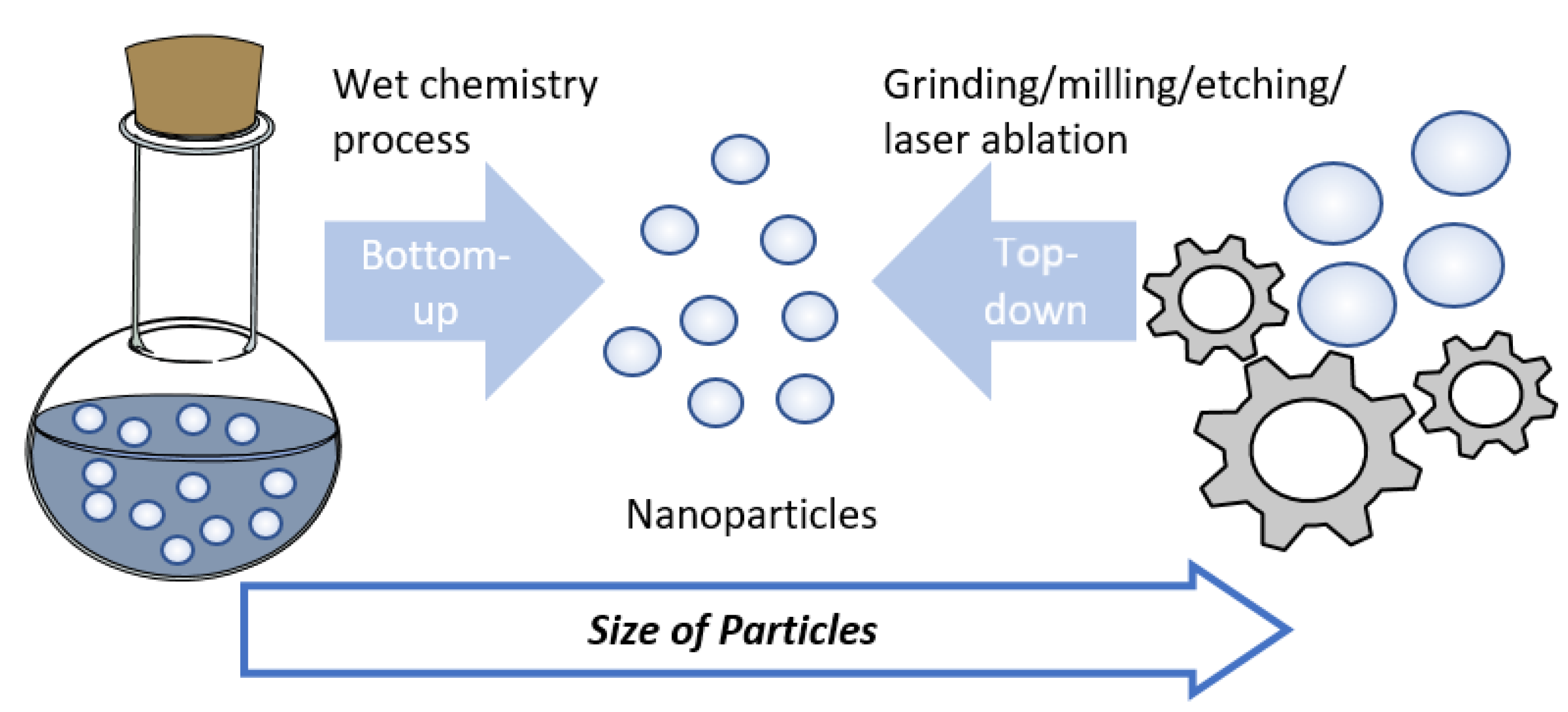
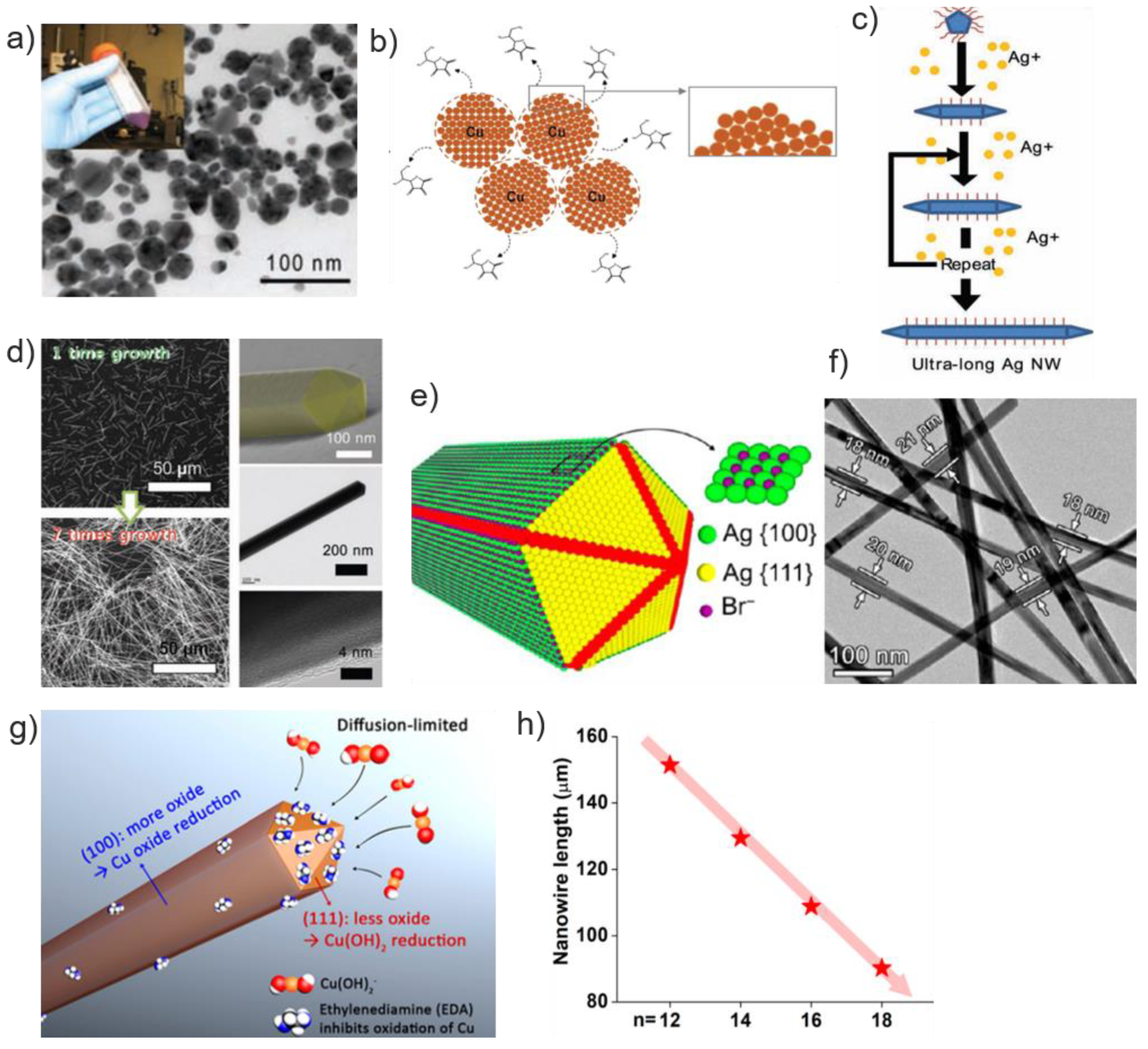
2.1. Metal Nanoparticles (NPs)
2.2. Metal Nanowires (NWs)
2.2.1. AgNWs
2.2.2. CuNWs
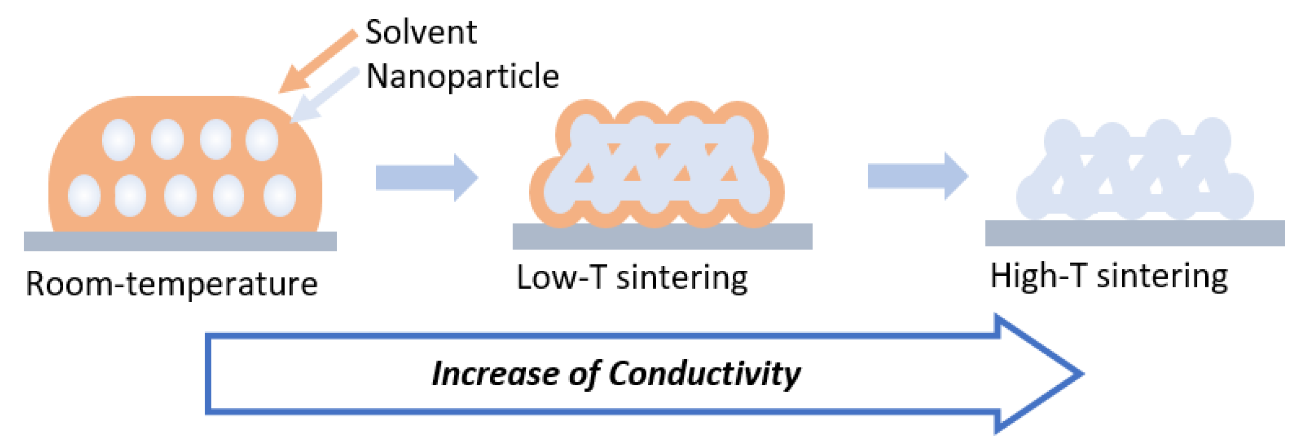
2.2.3. Post-Printing Treatment
2.3. Carbon Nanomaterials
2.3.1. Graphene
2.3.2. Carbon Nanotubes (CNTs)
2.4. Semiconductors
3. Printing Technologies
3.1. Non-Contact Printing Technologies
3.1.1. Inkjet Printing
3.1.2. Electrohydrodynamic (EHD) Printing
3.1.3. Aerosol Printing
3.2. Contact Printing Technologies
3.2.1. Screen Printing
3.2.2. Gravure Printing
3.2.3. Flexographic Printing
3.3. Strategies for High-Throughput Printing Devices (PEs)
3.3.1. High-Resolution Patterning
3.3.2. Uniformity
3.3.3. Flexibility/Stretchability
3.3.4. Durability
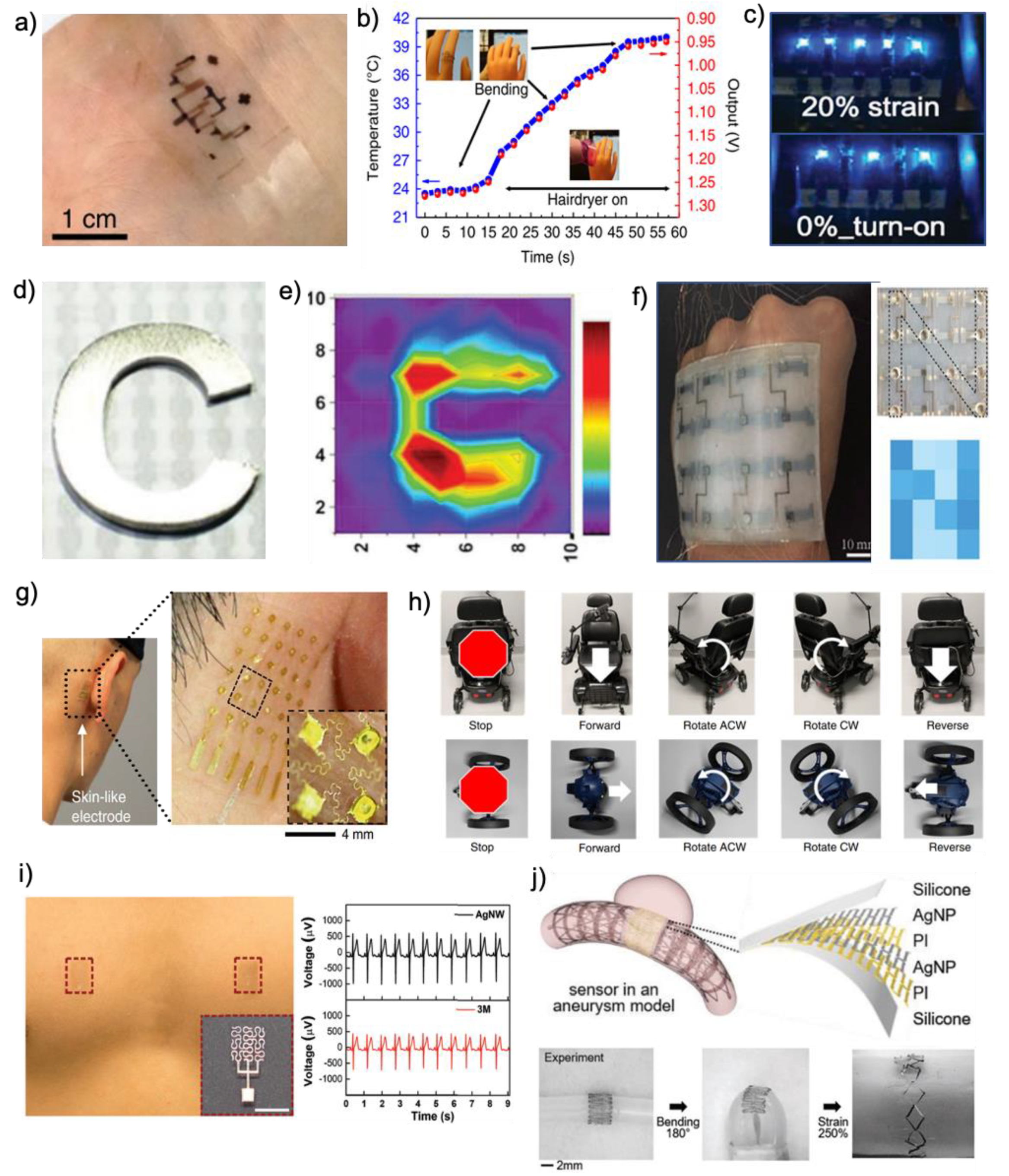
4. Applications
4.1. Nanomaterial-Enabled Sensors
4.1.1. Temperature Sensors
4.1.2. Strain/Pressure Sensors
4.1.3. Electrochemical Sensors
4.1.4. Electrophysiological Sensors
4.2. Printed Electronics
4.2.1. Prosthesis
4.2.2. Healthcare
4.2.3. Implantation
5. Conclusions and Outlook
Author Contributions
Funding
Conflicts of Interest
References
- Cummins, G.; Desmulliez, M.P.Y. Inkjet printing of conductive materials: A review. Circuit World 2012, 38, 193–213. [Google Scholar] [CrossRef]
- Ray, T.R.; Choi, J.; Bandodkar, A.J.; Krishnan, S.; Gutruf, P.; Tian, L.; Ghaffari, R.; Rogers, J.A. Bio-integrated wearable systems: A comprehensive review. Chem. Rev. 2019, 119, 5461–5533. [Google Scholar] [CrossRef] [PubMed]
- Jayathilaka, W.A.D.M.; Qi, K.; Qin, Y.; Chinnappan, A.; Serrano-García, W.; Baskar, C.; Wang, H.; He, J.; Cui, S.; Thomas, S.W.; et al. Significance of Nanomaterials in Wearables: A Review on Wearable Actuators and Sensors. Adv. Mater. 2019, 31, 1–21. [Google Scholar] [CrossRef] [PubMed]
- Huang, Q.; Zhu, Y. Printing Conductive Nanomaterials for Flexible and Stretchable Electronics: A Review of Materials, Processes, and Applications. Adv. Mater. Technol. 2019, 4, 1–41. [Google Scholar] [CrossRef]
- Li, H.; Liang, J. Recent Development of Printed Micro-Supercapacitors: Printable Materials, Printing Technologies, and Perspectives. Adv. Mater. 2020, 32, 1–19. [Google Scholar] [CrossRef] [PubMed]
- Wu, W. Inorganic nanomaterials for printed electronics: A review. Nanoscale 2017, 9, 7342–7372. [Google Scholar] [CrossRef]
- Kamyshny, A.; Magdassi, S. Conductive nanomaterials for 2D and 3D printed flexible electronics. Chem. Soc. Rev. 2019, 48, 1712–1740. [Google Scholar] [CrossRef]
- Stringer, J.; Derby, B. Formation and stability of lines produced by inkjet printing. Langmuir 2010, 26, 10365–10372. [Google Scholar] [CrossRef]
- Liu, M.; Wang, J.; He, M.; Wang, L.; Li, F.; Jiang, L.; Song, Y. Inkjet printing controllable footprint lines by regulating the dynamic wettability of coalescing ink droplets. ACS Appl. Mater. Interfaces 2014, 6, 13344–13348. [Google Scholar] [CrossRef]
- Kim, S.; Sojoudi, H.; Zhao, H.; Mariappan, D.; McKinley, G.H.; Gleason, K.K.; Hart, A.J. Ultrathin high-resolution flexographic printing using nanoporous stamps. Sci. Adv. 2016, 2. [Google Scholar] [CrossRef]
- Khan, S.; Lorenzelli, L.; Dahiya, R.S. Technologies for printing sensors and electronics over large flexible substrates: A review. IEEE Sens. J. 2015, 15, 3164–3185. [Google Scholar] [CrossRef]
- Fukuda, K.; Takeda, Y.; Yoshimura, Y.; Shiwaku, R.; Tran, L.T.; Sekine, T.; Mizukami, M.; Kumaki, D.; Tokito, S. Fully-printed high-performance organic thin-film transistors and circuitry on one-micron-thick polymer films. Nat. Commun. 2014, 5, 1–8. [Google Scholar] [CrossRef] [PubMed]
- Joo, S.J.; Park, S.H.; Moon, C.J.; Kim, H.S. A Highly Reliable Copper Nanowire/Nanoparticle Ink Pattern with High Conductivity on Flexible Substrate Prepared via a Flash Light-Sintering Technique. ACS Appl. Mater. Interfaces 2015, 7, 5674–5684. [Google Scholar] [CrossRef] [PubMed]
- Sullivan, M. Printed Electronics: Global Markets to 2022; BCC Res: Wellesley, MA, USA, 2018. [Google Scholar]
- Chen, Y.; Kim, Y.S.; Tillman, B.W.; Yeo, W.H.; Chun, Y. Advances in materials for recent low-profile implantable bioelectronics. Materials (Basel). 2018, 11, 1–24. [Google Scholar] [CrossRef] [PubMed]
- Kim, J.; Kumar, R.; Bandodkar, A.J.; Wang, J. Advanced Materials for Printed Wearable Electrochemical Devices: A Review. Adv. Electron. Mater. 2017, 3, 1–15. [Google Scholar] [CrossRef]
- Yao, S.; Swetha, P.; Zhu, Y. Nanomaterial-Enabled Wearable Sensors for Healthcare. Adv. Healthc. Mater. 2018, 7, 1–27. [Google Scholar] [CrossRef]
- Herbert, R.; Kim, J.H.; Kim, Y.S.; Lee, H.M.; Yeo, W.H. Soft material-enabled, flexible hybrid electronics for medicine, healthcare, and human-machine interfaces. Materials (Basel). 2018, 11. [Google Scholar] [CrossRef]
- Reineck, P.; Lin, Y.; Gibson, B.C.; Dickey, M.D.; Greentree, A.D.; Maksymov, I.S. UV plasmonic properties of colloidal liquid-metal eutectic gallium-indium alloy nanoparticles. Sci. Rep. 2019, 9, 1–7. [Google Scholar] [CrossRef]
- Prasek, J.; Drbohlavova, J.; Chomoucka, J.; Hubalek, J.; Jasek, O.; Adam, V.; Kizek, R. Methods for carbon nanotubes synthesis - Review. J. Mater. Chem. 2011, 21, 15872–15884. [Google Scholar] [CrossRef]
- Sadowski, J.; Kret, S.; Šiušys, A.; Wojciechowski, T.; Gas, K.; Islam, M.F.; Canali, C.M.; Sawicki, M. Wurtzite (Ga,Mn)As nanowire shells with ferromagnetic properties. Nanoscale 2017, 9, 2129–2137. [Google Scholar] [CrossRef]
- Tomchenko, A.A. Printed Chemical Sensors: From Screen- Printing to Microprinting ∗. Encycl. Sens. 2006, 10, 279–290. [Google Scholar]
- Herbert, R.; Mishra, S.; Lim, H.R.; Yoo, H.; Yeo, W.H. Fully Printed, Wireless, Stretchable Implantable Biosystem toward Batteryless, Real-Time Monitoring of Cerebral Aneurysm Hemodynamics. Adv. Sci. 2019, 6. [Google Scholar] [CrossRef] [PubMed]
- Fu, S.; Tao, J.; Wu, W.; Sun, J.; Li, F.; Li, J.; Huo, Z.; Xia, Z.; Bao, R.; Pan, C. Fabrication of Large-Area Bimodal Sensors by All-Inkjet-Printing. Adv. Mater. Technol. 2019, 4, 1–9. [Google Scholar] [CrossRef]
- Zhu, C.; Chortos, A.; Wang, Y.; Pfattner, R.; Lei, T.; Hinckley, A.C.; Pochorovski, I.; Yan, X.; To, J.W.F.; Oh, J.Y.; et al. Stretchable temperature-sensing circuits with strain suppression based on carbon nanotube transistors. Nat. Electron. 2018, 1, 183–190. [Google Scholar] [CrossRef]
- Kim, S.; Byun, J.; Choi, S.; Kim, D.; Kim, T.; Chung, S.; Hong, Y. Negatively strain-dependent electrical resistance of magnetically arranged nickel composites: Application to highly stretchable electrodes and stretchable lighting devices. Adv. Mater. 2014, 26, 3094–3099. [Google Scholar] [CrossRef]
- Mishra, S.; Kim, Y.S.; Intarasirisawat, J.; Kwon, Y.T.; Lee, Y.; Mahmood, M.; Lim, H.R.; Herbert, R.; Yu, K.J.; Ang, C.S.; et al. Soft, wireless periocular wearable electronics for real-time detection of eye vergence in a virtual reality toward mobile eye therapies. Sci. Adv. 2020, 6. [Google Scholar] [CrossRef]
- Cui, Z.; Han, Y.; Huang, Q.; Dong, J.; Zhu, Y. Electrohydrodynamic printing of silver nanowires for flexible and stretchable electronics. Nanoscale 2018, 10, 6806–6811. [Google Scholar] [CrossRef]
- Mahmood, M.; Mzurikwao, D.; Kim, Y.-S.; Lee, Y.; Mishra, S.; Herbert, R.; Duarte, A.; Ang, C.S.; Yeo, W.-H. Fully portable and wireless universal brain–machine interfaces enabled by flexible scalp electronics and deep learning algorithm. Nat. Mach. Intell. 2019, 1, 412–422. [Google Scholar] [CrossRef]
- Buzea, C.; Pacheco, I.I.; Robbie, K. Nanomaterials and nanoparticles: Sources and toxicity. Biointerphases 2007, 2, MR17–MR71. [Google Scholar] [CrossRef]
- Abulikemu, M.; Da’as, E.H.; Haverinen, H.; Cha, D.; Malik, M.A.; Jabbour, G.E. In Situ Synthesis of Self-Assembled Gold Nanoparticles on Glass or Silicon Substrates through Reactive Inkjet Printing. Angew. Chem. 2014, 126, 430–433. [Google Scholar] [CrossRef]
- Kwon, Y.-T.; Yune, S.-J.; Song, Y.; Yeo, W.-H.; Choa, Y.-H. Green Manufacturing of Highly Conductive Cu 2 O and Cu Nanoparticles for Photonic-Sintered Printed Electronics. ACS Appl. Electron. Mater. 2019, 1, 2069–2075. [Google Scholar] [CrossRef]
- Jeong, S.; Lee, S.H.; Jo, Y.; Lee, S.S.; Seo, Y.H.; Ahn, B.W.; Kim, G.; Jang, G.E.; Park, J.U.; Ryu, B.H.; et al. Air-stable, surface-oxide free Cu nanoparticles for highly conductive Cu ink and their application to printed graphene transistors. J. Mater. Chem. C 2013, 1, 2704–2710. [Google Scholar] [CrossRef]
- Rahman, M.T.; Cheng, C.Y.; Karagoz, B.; Renn, M.; Schrandt, M.; Gellman, A.; Panat, R. High Performance Flexible Temperature Sensors via Nanoparticle Printing. ACS Appl. Nano Mater. 2019, 2, 3280–3291. [Google Scholar] [CrossRef]
- Roberts, R.C.; Tien, N.C. Multilayer passive rf microfabrication using jet-printed au nanoparticle ink and aerosol-deposited dielectric department of electrical and electronic engineering. In Proceedings of the 2013 Transducers Eurosensors XXVII 17th Int. Conf. Solid-State Sensors, Actuators Microsystems, Barcelona, Spain, 16–20 June 2013; pp. 178–181. [Google Scholar]
- Shariq, M.; Chattopadhyaya, S.; Rudolf, R.; Rai Dixit, A. Characterization of AuNPs based ink for inkjet printing of low cost paper based sensors. Mater. Lett. 2020, 264, 127332. [Google Scholar] [CrossRef]
- Qin, Y.; Alam, A.U.; Howlader, M.M.R.; Hu, N.X.; Deen, M.J. Inkjet Printing of a Highly Loaded Palladium Ink for Integrated, Low-Cost pH Sensors. Adv. Funct. Mater. 2016, 26, 4923–4933. [Google Scholar] [CrossRef]
- Tseng, C.C.; Chang, C.P.; Sung, Y.; Chen, Y.C.; Ger, M. Der A novel method to produce Pd nanoparticle ink for ink-jet printing technology. Colloids Surfaces A Physicochem. Eng. Asp. 2009, 339, 206–210. [Google Scholar] [CrossRef]
- Rajan, K.; Roppolo, I.; Chiappone, A.; Bocchini, S.; Perrone, D.; Chiolerio, A. Silver nanoparticle ink technology: State of the art. Nanotechnol. Sci. Appl. 2016, 9, 1–13. [Google Scholar] [CrossRef]
- Gao, M.; Li, L.; Song, Y. Inkjet printing wearable electronic devices. J. Mater. Chem. C 2017, 5, 2971–2993. [Google Scholar] [CrossRef]
- Choi, S.; Han, S.I.; Jung, D.; Hwang, H.J.; Lim, C.; Bae, S.; Park, O.K.; Tschabrunn, C.M.; Lee, M.; Bae, S.Y.; et al. Highly conductive, stretchable and biocompatible Ag–Au core–sheath nanowire composite for wearable and implantable bioelectronics. Nat. Nanotechnol. 2018, 13, 1048–1056. [Google Scholar] [CrossRef]
- Jung, I.; Jo, Y.H.; Kim, I.; Lee, H.M. A simple process for synthesis of Ag nanoparticles and sintering of conductive ink for use in printed electronics. J. Electron. Mater. 2012, 41, 115–121. [Google Scholar] [CrossRef]
- Gutel, T.; Garcia-Antõn, J.; Pelzer, K.; Philippot, K.; Santini, C.C.; Chauvin, Y.; Chaudret, B.; Basset, J.-M. Influence of the self-organization of ionic liquids on the size of ruthenium nanoparticles: Effect of the temperature and stirring. J. Mater. Chem. 2007, 17, 3290–3292. [Google Scholar] [CrossRef]
- Zhang, Z.; Zhang, X.; Xin, Z.; Deng, M.; Wen, Y.; Song, Y. Synthesis of monodisperse silver nanoparticles for ink-jet printed flexible electronics. Nanotechnology 2011, 22. [Google Scholar] [CrossRef] [PubMed]
- Ahn, B.Y.; Duoss, E.B.; Motala, M.J.; Guo, X.; Park, S., II; Xiong, Y.; Yoon, J.; Nuzzo, R.G.; Rogers, J.A.; Lewis, J.A. Omnidirectional printing of flexible, stretchable, and spanning silver microelectrodes. Science 2009, 323, 1590–1593. [Google Scholar] [CrossRef] [PubMed]
- Yang, X.; He, W.; Wang, S.; Zhou, G.; Tang, Y.; Yang, J. Effect of the different shapes of silver particles in conductive ink on electrical performance and microstructure of the conductive tracks. J. Mater. Sci. Mater. Electron. 2012, 23, 1980–1986. [Google Scholar] [CrossRef]
- Chen, S.; Guan, Y.; Li, Y.; Yan, X.; Ni, H.; Li, L. A water-based silver nanowire ink for large-scale flexible transparent conductive films and touch screens. J. Mater. Chem. C 2017, 5, 2404–2414. [Google Scholar] [CrossRef]
- Määttänen, A.; Ihalainen, P.; Pulkkinen, P.; Wang, S.; Tenhu, H.; Peltonen, J. Inkjet-printed gold electrodes on paper: Characterization and functionalization. ACS Appl. Mater. Interfaces 2012, 4, 955–964. [Google Scholar] [CrossRef]
- Hwang, H.; Kim, A.; Zhong, Z.; Kwon, H.C.; Jeong, S.; Moon, J. Reducible-Shell-Derived Pure-Copper-Nanowire Network and Its Application to Transparent Conducting Electrodes. Adv. Funct. Mater. 2016, 26, 6545–6554. [Google Scholar] [CrossRef]
- Lee, P.; Lee, J.; Lee, H.; Yeo, J.; Hong, S.; Nam, K.H.; Lee, D.; Lee, S.S.; Ko, S.H. Highly stretchable and highly conductive metal electrode by very long metal nanowire percolation network. Adv. Mater. 2012, 24, 3326–3332. [Google Scholar] [CrossRef]
- Da Silva, R.R.; Yang, M.; Choi, S., II; Chi, M.; Luo, M.; Zhang, C.; Li, Z.Y.; Camargo, P.H.C.; Ribeiro, S.J.L.; Xia, Y. Facile Synthesis of Sub-20 nm Silver Nanowires through a Bromide-Mediated Polyol Method. ACS Nano 2016, 10, 7892–7900. [Google Scholar] [CrossRef]
- Kim, M.J.; Flowers, P.F.; Stewart, I.E.; Ye, S.; Baek, S.; Kim, J.J.; Wiley, B.J. Ethylenediamine promotes Cu nanowire growth by inhibiting oxidation of Cu(111). J. Am. Chem. Soc. 2017, 139, 277–284. [Google Scholar] [CrossRef]
- Kim, M.J.; Alvarez, S.; Yan, T.; Tadepalli, V.; Fichthorn, K.A.; Wiley, B.J. Modulating the Growth Rate, Aspect Ratio, and Yield of Copper Nanowires with Alkylamines. Chem. Mater. 2018, 30, 2809–2818. [Google Scholar] [CrossRef]
- Maisch, P.; Tam, K.C.; Lucera, L.; Egelhaaf, H.J.; Scheiber, H.; Maier, E.; Brabec, C.J. Inkjet printed silver nanowire percolation networks as electrodes for highly efficient semitransparent organic solar cells. Org. Electron. 2016, 38, 139–143. [Google Scholar] [CrossRef]
- Hsu, P.C.; Wang, S.; Wu, H.; Narasimhan, V.K.; Kong, D.; Ryoung Lee, H.; Cui, Y. Performance enhancement of metal nanowire transparent conducting electrodes by mesoscale metal wires. Nat. Commun. 2013, 4, 1–7. [Google Scholar] [CrossRef] [PubMed]
- Mutiso, R.M.; Sherrott, M.C.; Rathmell, A.R.; Wiley, B.J.; Winey, K.I. Integrating simulations and experiments to predict sheet resistance and optical transmittance in nanowire films for transparent conductors. ACS Nano 2013, 7, 7654–7663. [Google Scholar] [CrossRef] [PubMed]
- Yang, W.; Li, N.W.; Zhao, S.; Yuan, Z.; Wang, J.; Du, X.; Wang, B.; Cao, R.; Li, X.; Xu, W.; et al. A Breathable and Screen-Printed Pressure Sensor Based on Nanofiber Membranes for Electronic Skins. Adv. Mater. Technol. 2018, 3, 1–7. [Google Scholar] [CrossRef]
- He, W.; Ye, C. Flexible Transparent Conductive Films on the Basis of Ag Nanowires: Design and Applications: A Review. J. Mater. Sci. Technol. 2015, 31, 581–588. [Google Scholar] [CrossRef]
- Rycenga, M.; Cobley, C.M.; Zeng, J.; Li, W.; Moran, C.H.; Zhang, Q.; Qin, D.; Xia, Y. Controlling the synthesis and assembly of silver nanostructures for plasmonic applications. Chem. Rev. 2011, 111, 3669–3712. [Google Scholar] [CrossRef]
- Wiley, B.; Sun, Y.; Xia, Y. Synthesis of silver nanostructures with controlled shapes and properties. Acc. Chem. Res. 2007, 40, 1067–1076. [Google Scholar] [CrossRef]
- Schuette, W.M.; Buhro, W.E. Polyol synthesis of silver nanowires by heterogeneous nucleation; Mechanistic aspects influencing nanowire diameter and length. Chem. Mater. 2014, 26, 6410–6417. [Google Scholar] [CrossRef]
- Rathmell, A.R.; Bergin, S.M.; Hua, Y.L.; Li, Z.Y.; Wiley, B.J. The growth mechanism of copper nanowires and their properties in flexible, transparent conducting films. Adv. Mater. 2010, 22, 3558–3563. [Google Scholar] [CrossRef]
- Schriver, M.; Regan, W.; Gannett, W.J.; Zaniewski, A.M.; Crommie, M.F.; Zettl, A. Graphene as a long-term metal oxidation barrier: Worse than nothing. ACS Nano 2013, 7, 5763–5768. [Google Scholar] [CrossRef] [PubMed]
- Niu, Z.; Cui, F.; Yu, Y.; Becknell, N.; Sun, Y.; Khanarian, G.; Kim, D.; Dou, L.; Dehestani, A.; Schierle-Arndt, K.; et al. Ultrathin Epitaxial Cu@Au Core-Shell Nanowires for Stable Transparent Conductors. J. Am. Chem. Soc. 2017, 139, 7348–7354. [Google Scholar] [CrossRef] [PubMed]
- Allen, M.L.; Aronniemi, M.; Mattila, T.; Alastalo, A.; Ojanperä, K.; Suhonen, M.; Seppä, H. Electrical sintering of nanoparticle structures. Nanotechnology 2008, 19, 175201. [Google Scholar] [CrossRef] [PubMed]
- Tsumaki, M.; Nitta, K.; Jeon, S.; Terashima, K.; Ito, T. Development of plasma-assisted inkjet printing and demonstration for direct printing of conductive silver line. J. Phys. D. Appl. Phys. 2018, 51, 30LT01. [Google Scholar] [CrossRef]
- Zhong, Z.; Lee, S.H.; Ko, P.; Kwon, S.; Youn, H.; Seok, J.Y.; Woo, K. Control of thermal deformation with photonic sintering of ultrathin nanowire transparent electrodes. Nanoscale 2020, 12, 2366–2373. [Google Scholar] [CrossRef]
- Jung, S.; Chun, S.J.; Shon, C.-H. Rapid cellulose-mediated microwave sintering for high-conductivity Ag patterns on paper. ACS Appl. Mater. Interfaces 2016, 8, 20301–20308. [Google Scholar] [CrossRef]
- Tavakoli, M.; Malakooti, M.H.; Paisana, H.; Ohm, Y.; Green Marques, D.; Alhais Lopes, P.; Piedade, A.P.; de Almeida, A.T.; Majidi, C. EGaIn-Assisted Room-Temperature Sintering of Silver Nanoparticles for Stretchable, Inkjet-Printed, Thin-Film Electronics. Adv. Mater. 2018, 30, 1–7. [Google Scholar] [CrossRef]
- Hyun, W.J.; Secor, E.B.; Hersam, M.C.; Frisbie, C.D.; Francis, L.F. High-resolution patterning of graphene by screen printing with a silicon stencil for highly flexible printed electronics. Adv. Mater. 2015, 27, 109–115. [Google Scholar] [CrossRef]
- Tuteja, S.K.; Ormsby, C.; Neethirajan, S. Noninvasive Label-Free Detection of Cortisol and Lactate Using Graphene Embedded Screen-Printed Electrode. Nano-Micro Lett. 2018, 10, 1–10. [Google Scholar] [CrossRef]
- Bellani, S.; Petroni, E.; Del Rio Castillo, A.E.; Curreli, N.; Martín-García, B.; Oropesa-Nuñez, R.; Prato, M.; Bonaccorso, F. Scalable Production of Graphene Inks via Wet-Jet Milling Exfoliation for Screen-Printed Micro-Supercapacitors. Adv. Funct. Mater. 2019, 29, 1–14. [Google Scholar] [CrossRef]
- Li, J.; Ye, F.; Vaziri, S.; Muhammed, M.; Lemme, M.C.; Östling, M. Efficient inkjet printing of graphene. Adv. Mater. 2013, 25, 3985–3992. [Google Scholar] [CrossRef] [PubMed]
- Torrisi, F.; Hasan, T.; Wu, W.; Sun, Z.; Lombardo, A.; Kulmala, T.S.; Hsieh, G.W.; Jung, S.; Bonaccorso, F.; Paul, P.J.; et al. Inkjet-printed graphene electronics. ACS Nano 2012, 6, 2992–3006. [Google Scholar] [CrossRef] [PubMed]
- Ciesielski, A.; Samorì, P. Graphene via sonication assisted liquid-phase exfoliation. Chem. Soc. Rev. 2014, 43, 381–398. [Google Scholar] [CrossRef] [PubMed]
- Fujigaya, T.; Nakashima, N. Methodology for homogeneous dispersion of single-walled carbon nanotubes by physical modification. Polym. J. 2008, 40, 577–589. [Google Scholar] [CrossRef]
- Schmidt, C.D.; Böttcher, C.; Hirsch, A. Synthesis and aggregation properties of water-soluble newkome-dendronized perylenetetracarboxdiimides. European J. Org. Chem. 2007, 2007, 5497–5505. [Google Scholar] [CrossRef]
- De, S.; King, P.J.; Lotya, M.; O’Neill, A.; Doherty, E.M.; Hernandez, Y.; Duesberg, G.S.; Coleman, J.N. Flexible, transparent, conducting films of randomly stacked graphene from surfactant-stabilized, oxide-free graphene dispersions. Small 2010, 6, 458–464. [Google Scholar] [CrossRef]
- Lotya, M.; Hernandez, Y.; King, P.J.; Smith, R.J.; Nicolosi, V.; Karlsson, L.S.; Blighe, F.M.; De, S.; Zhiming, W.; McGovern, I.T.; et al. Liquid phase production of graphene by exfoliation of graphite in surfactant/water solutions. J. Am. Chem. Soc. 2009, 131, 3611–3620. [Google Scholar] [CrossRef]
- Karagiannidis, P.G.; Hodge, S.A.; Lombardi, L.; Tomarchio, F.; Decorde, N.; Milana, S.; Goykhman, I.; Su, Y.; Mesite, S.V.; Johnstone, D.N.; et al. Microfluidization of Graphite and Formulation of Graphene-Based Conductive Inks. ACS Nano 2017, 11, 2742–2755. [Google Scholar] [CrossRef]
- Xiong, Z.; Yun, X.; Qiu, L.; Sun, Y.; Tang, B.; He, Z.; Xiao, J.; Chung, D.; Ng, T.W.; Yan, H.; et al. A Dynamic Graphene Oxide Network Enables Spray Printing of Colloidal Gels for High-Performance Micro-Supercapacitors. Adv. Mater. 2019, 31, 1–7. [Google Scholar] [CrossRef]
- Arapov, K.; Rubingh, E.; Abbel, R.; Laven, J.; de With, G.; Friedrich, H. Conductive Screen Printing Inks by Gelation of Graphene Dispersions. Adv. Funct. Mater. 2016, 26, 586–593. [Google Scholar] [CrossRef]
- Min, S.H.; Lee, G.Y.; Ahn, S.H. Direct printing of highly sensitive, stretchable, and durable strain sensor based on silver nanoparticles/multi-walled carbon nanotubes composites. Compos. Part B Eng. 2019, 161, 395–401. [Google Scholar] [CrossRef]
- Li, Q.; Li, Y.; Zhang, X.; Chikkannanavar, S.B.; Zhao, Y.; Dangelewicz, A.M.; Zheng, L.; Doorn, S.K.; Jia, Q.; Peterson, D.E.; et al. Structure-dependent electrical properties of carbon nanotube fibers. Adv. Mater. 2007, 19, 3358–3363. [Google Scholar] [CrossRef]
- Baby, T.T.; Garlapati, S.K.; Dehm, S.; Häming, M.; Kruk, R.; Hahn, H.; Dasgupta, S. A general route toward complete room temperature processing of printed and high performance oxide electronics. ACS Nano 2015, 9, 3075–3083. [Google Scholar] [CrossRef] [PubMed]
- Garlapati, S.K.; Gebauer, J.S.; Dehm, S.; Bruns, M.; Winterer, M.; Hahn, H.; Dasgupta, S. Room-Temperature Processing of Printed Oxide FETs Using Ultraviolet Photonic Curing. Adv. Electron. Mater. 2017, 3, 1–6. [Google Scholar] [CrossRef]
- Kim, T.Y.; Ha, J.; Cho, K.; Pak, J.; Seo, J.; Park, J.; Kim, J.K.; Chung, S.; Hong, Y.; Lee, T. Transparent Large-Area MoS2 Phototransistors with Inkjet-Printed Components on Flexible Platforms. ACS Nano 2017, 11, 10273–10280. [Google Scholar] [CrossRef]
- Wang, Y.; Yan, C.; Cheng, S.Y.; Xu, Z.Q.; Sun, X.; Xu, Y.H.; Chen, J.J.; Jiang, Z.; Liang, K.; Feng, Z.S. Flexible RFID Tag Metal Antenna on Paper-Based Substrate by Inkjet Printing Technology. Adv. Funct. Mater. 2019, 29, 1–11. [Google Scholar] [CrossRef]
- Derby, B. Inkjet Printing of Functional and Structural Materials: Fluid Property Requirements, Feature Stability, and Resolution. Annu. Rev. Mater. Res. 2010, 40, 395–414. [Google Scholar] [CrossRef]
- Liu, X.; Tarn, T.J.; Huang, F.; Fan, J. Recent advances in inkjet printing synthesis of functional metal oxides. Particuology 2015, 19, 1–13. [Google Scholar] [CrossRef]
- Deegan, R.D.; Bakajin, O.; Dupont, T.F.; Huber, G.; Nagel, S.R.; Witten, T.A. Capillary flow as the cause of ring stains from dried liquid drops. Nature 1997, 389, 827–829. [Google Scholar] [CrossRef]
- Zhang, Z.; Zhang, X.; Xin, Z.; Deng, M.; Wen, Y.; Song, Y. Controlled inkjetting of a conductive pattern of silver nanoparticles based on the coffee-ring effect. Adv. Mater. 2013, 25, 6714–6718. [Google Scholar] [CrossRef]
- Layani, M.; Gruchko, M.; Milo, O.; Balberg, I.; Azulay, D.; Magdassi, S. Transparent conductive coatings by printing coffee ring arrays obtained at room temperature. ACS Nano 2009, 3, 3537–3542. [Google Scholar] [CrossRef] [PubMed]
- Kuang, M.; Wang, L.; Song, Y. Controllable Printing Droplets for High-Resolution Patterns. Adv. Mater. 2014, 26, 6950–6958. [Google Scholar] [CrossRef] [PubMed]
- Cai, L.; Zhang, S.; Zhang, Y.; Li, J.; Miao, J.; Wang, Q.; Yu, Z.; Wang, C. Direct Printing for Additive Patterning of Silver Nanowires for Stretchable Sensor and Display Applications. Adv. Mater. Technol. 2018, 3, 1–8. [Google Scholar] [CrossRef]
- Shimoni, A.; Azoubel, S.; Magdassi, S. Inkjet printing of flexible high-performance carbon nanotube transparent conductive films by “coffee ring effect”. Nanoscale 2014, 6, 11084–11089. [Google Scholar] [CrossRef] [PubMed]
- Kuang, M.; Wang, J.; Bao, B.; Li, F.; Wang, L.; Jiang, L.; Song, Y. Inkjet Printing Patterned Photonic Crystal Domes for Wide Viewing-Angle Displays by Controlling the Sliding Three Phase Contact Line. Adv. Opt. Mater. 2014, 2, 34–38. [Google Scholar] [CrossRef]
- Wei, Y.; Chen, S.; Li, F.; Lin, Y.; Zhang, Y.; Liu, L. Highly Stable and Sensitive Paper-Based Bending Sensor Using Silver Nanowires/Layered Double Hydroxides Hybrids. ACS Appl. Mater. Interfaces 2015, 7, 14182–14191. [Google Scholar] [CrossRef]
- Chen, S.P.; Durán Retamal, J.R.; Lien, D.H.; He, J.H.; Liao, Y.C. Inkjet-printed transparent nanowire thin film features for UV photodetectors. RSC Adv. 2015, 5, 70707–70712. [Google Scholar] [CrossRef]
- McManus, D.; Vranic, S.; Withers, F.; Sanchez-Romaguera, V.; Macucci, M.; Yang, H.; Sorrentino, R.; Parvez, K.; Son, S.K.; Iannaccone, G.; et al. Water-based and biocompatible 2D crystal inks for all-inkjet-printed heterostructures. Nat. Nanotechnol. 2017, 12, 343–350. [Google Scholar] [CrossRef]
- Parvez, K.; Worsley, R.; Alieva, A.; Felten, A.; Casiraghi, C. Water-based and inkjet printable inks made by electrochemically exfoliated graphene. Carbon N. Y. 2019, 149, 213–221. [Google Scholar] [CrossRef]
- Karim, N.; Afroj, S.; Tan, S.; Novoselov, K.S.; Yeates, S.G. All Inkjet-Printed Graphene-Silver Composite Ink on Textiles for Highly Conductive Wearable Electronics Applications. Sci. Rep. 2019, 9, 1–10. [Google Scholar] [CrossRef]
- Lim, H.R.; Kim, H.S.; Qazi, R.; Kwon, Y.T.; Jeong, J.W.; Yeo, W.H. Advanced Soft Materials, Sensor Integrations, and Applications of Wearable Flexible Hybrid Electronics in Healthcare, Energy, and Environment. Adv. Mater. 2019, 1901924, 1–43. [Google Scholar] [CrossRef]
- Zhang, Y.Z.; Wang, Y.; Jiang, Q.; El-Demellawi, J.K.; Kim, H.; Alshareef, H.N. MXene Printing and Patterned Coating for Device Applications. Adv. Mater. 2020, 32, 1–26. [Google Scholar] [CrossRef] [PubMed]
- Wang, B.; Facchetti, A. Mechanically Flexible Conductors for Stretchable and Wearable E-Skin and E-Textile Devices. Adv. Mater. 2019, 31, 1–53. [Google Scholar] [CrossRef] [PubMed]
- Zhang, C. (John); McKeon, L.; Kremer, M.P.; Park, S.H.; Ronan, O.; Seral--Ascaso, A.; Barwich, S.; Coileáin, C.; McEvoy, N.; Nerl, H.C.; et al. Additive-free MXene inks and direct printing of micro-supercapacitors. Nat. Commun. 2019, 10, 1–9. [Google Scholar] [CrossRef]
- Vural, M.; Pena-Francesch, A.; Bars-Pomes, J.; Jung, H.; Gudapati, H.; Hatter, C.B.; Allen, B.D.; Anasori, B.; Ozbolat, I.T.; Gogotsi, Y.; et al. Inkjet Printing of Self-Assembled 2D Titanium Carbide and Protein Electrodes for Stimuli-Responsive Electromagnetic Shielding. Adv. Funct. Mater. 2018, 28, 1–10. [Google Scholar] [CrossRef]
- Jiang, X.; Li, W.; Hai, T.; Yue, R.; Chen, Z.; Lao, C.; Ge, Y.; Xie, G.; Wen, Q.; Zhang, H. Inkjet-printed MXene micro-scale devices for integrated broadband ultrafast photonics. NPJ 2D Mater. Appl. 2019, 3. [Google Scholar] [CrossRef]
- Li, J.; Naiini, M.M.; Vaziri, S.; Lemme, M.C.; Östling, M. Inkjet printing of MoS2. Adv. Funct. Mater. 2014, 24, 6524–6531. [Google Scholar] [CrossRef]
- Chen, B.; Das, S.R.; Zheng, W.; Zhu, B.; Xu, B.; Hong, S.; Sun, C.; Wang, X.; Wu, Y.; Claussen, J.C. Inkjet Printing of Single-Crystalline Bi2Te3 Thermoelectric Nanowire Networks. Adv. Electron. Mater. 2017, 3. [Google Scholar] [CrossRef]
- Yuk, H.; Lu, B.; Lin, S.; Qu, K.; Xu, J.; Luo, J.; Zhao, X. 3D printing of conducting polymers. Nat. Commun. 2020, 11, 4–11. [Google Scholar] [CrossRef]
- Oh, Y.; Bharambe, V.; Mummareddy, B.; Martin, J.; McKnight, J.; Abraham, M.A.; Walker, J.M.; Rogers, K.; Conner, B.; Cortes, P.; et al. Microwave dielectric properties of zirconia fabricated using NanoParticle JettingTM. Addit. Manuf. 2019, 27, 586–594. [Google Scholar] [CrossRef]
- Png, K.; Lei, L. Nanodimension Minipaper: Gaining Strategic Advantage in RFID Antenna Manufacturing; Nano Dimension Ltd.: Ness Ziona, Central Israel, Israel, 2017. [Google Scholar]
- Park, J.U.; Hardy, M.; Kang, S.J.; Barton, K.; Adair, K.; Mukhopadhyay, D.K.; Lee, C.Y.; Strano, M.S.; Alleyne, A.G.; Georgiadis, J.G.; et al. High-resolution electrohydrodynamic jet printing. Nat. Mater. 2007, 6, 782–789. [Google Scholar] [CrossRef] [PubMed]
- He, J.; Xu, F.; Dong, R.; Guo, B.; Li, D. Electrohydrodynamic 3D printing of microscale poly (ϵ-caprolactone) scaffolds with multi-walled carbon nanotubes. Biofabrication 2017, 9. [Google Scholar] [CrossRef] [PubMed]
- Han, Y.; Dong, J. Electrohydrodynamic (EHD) Printing of Molten Metal Ink for Flexible and Stretchable Conductor with Self-Healing Capability. Adv. Mater. Technol. 2018, 3, 1700268. [Google Scholar] [CrossRef]
- Collins, R.T.; Harris, M.T.; Basaran, O.A. Breakup of electrified jets. J. Fluid Mech. 2007, 588, 75–129. [Google Scholar] [CrossRef]
- Zhang, B.; He, J.; Li, X.; Xu, F.; Li, D. Micro/nanoscale electrohydrodynamic printing: From 2D to 3D. Nanoscale 2016, 8, 15376–15388. [Google Scholar] [CrossRef]
- Chang, J.; He, J.; Lei, Q.; Li, D. Electrohydrodynamic Printing of Microscale PEDOT:PSS-PEO Features with Tunable Conductive/Thermal Properties. ACS Appl. Mater. Interfaces 2018, 10, 19116–19122. [Google Scholar] [CrossRef]
- Darrieutort, B.; Pellet, C.; Pibre, G.; Ayela, C. Elaboration of soft and flexible silicone stencils for the wafer-level micropatterning of polymers. J. Micromech. Microeng. 2006, 17, 2–3. [Google Scholar] [CrossRef]
- Pan, Y.; Chen, X.; Zeng, L.; Huang, Y.; Yin, Z. Fabrication and evaluation of a protruding Si-based printhead for electrohydrodynamic jet printing. J. Micromech. Microeng. 2017, 27, 125004. [Google Scholar] [CrossRef]
- Liang, J.S.; Zhang, Y.; Wang, D.Z.; Luo, T.P.; Ren, T.Q. A novel compact heat exchanger using gap flow mechanism. Rev. Sci. Instrum. 2015, 86, 024904. [Google Scholar] [CrossRef]
- Wang, D.; Zhao, X.; Lin, Y.; Liang, J.; Ren, T.; Liu, Z.; Li, J. Nanoscale coaxial focused electrohydrodynamic jet printing. Nanoscale 2018, 10, 9867–9879. [Google Scholar] [CrossRef]
- Zou, W.; Yu, H.; Zhou, P.; Liu, L. Tip-assisted electrohydrodynamic jet printing for high-resolution microdroplet deposition. Mater. Des. 2019, 166, 107609. [Google Scholar] [CrossRef]
- Jang, Y.; Kim, J.; Byun, D. Invisible metal-grid transparent electrode prepared by electrohydrodynamic (EHD) jet printing. J. Phys. D Appl. Phys. 2013, 46. [Google Scholar] [CrossRef]
- Zhang, B.; Seong, B.; Lee, J.; Nguyen, V.; Cho, D.; Byun, D. One-Step Sub-micrometer-Scale Electrohydrodynamic Inkjet Three-Dimensional Printing Technique with Spontaneous Nanoscale Joule Heating. ACS Appl. Mater. Interfaces 2017, 9, 29965–29972. [Google Scholar] [CrossRef]
- Morales-Rodriguez, M.E.; Joshi, P.C.; Humphries, J.R.; Fuhr, P.L.; McIntyre, T.J. Fabrication of low cost surface acoustic wave sensors using direct printing by aerosol inkjet. IEEE Access 2018, 6, 20907–20915. [Google Scholar] [CrossRef]
- Ou, C.; Sangle, A.L.; Chalklen, T.; Jing, Q.; Narayan, V.; Kar-Narayan, S. Enhanced thermoelectric properties of flexible aerosol-jet printed carbon nanotube-based nanocomposites. APL Mater. 2018, 6, 096101. [Google Scholar] [CrossRef]
- Rahman, T.; Renaud, L.; Heo, D.; Renn, M.; Panat, R. Aerosol based direct-write micro-additive fabrication method for sub-mm 3D metal-dielectric structures. J. Micromech. Microeng. 2015, 25. [Google Scholar] [CrossRef]
- Lall, P.; Abrol, A.; Kothari, N.; Leever, B.; Miller, S. Effect of Print Parameters on Print Consistency of Aerosol Jet Printed Electronics. In Proceedings of the 2019 18th IEEE Intersociety Conference on Thermal and Thermomechanical Phenomena in Electronic Systems (ITherm), Las Vegas, NV, USA, 28–31 May 2019; pp. 633–642. [Google Scholar]
- Mahajan, A.; Frisbie, C.D.; Francis, L.F. Optimization of aerosol jet printing for high-resolution, high-aspect ratio silver lines. ACS Appl. Mater. Interfaces 2013, 5, 4856–4864. [Google Scholar] [CrossRef]
- Smith, M.; Choi, Y.S.; Boughey, C.; Kar-Narayan, S. Controlling and assessing the quality of aerosol jet printed features for large area and flexible electronics. Flex. Print. Electron. 2017, 2. [Google Scholar] [CrossRef]
- Paulsen, J.A.; Renn, M.; Christenson, K.; Plourde, R. Printing conformal electronics on 3D structures with aerosol jet technology. FIIW 2012—2012 Futur. Instrum. Int. Work. Proc. 2012, 47–50. [Google Scholar] [CrossRef]
- Gandhiraman, R.P.; Jayan, V.; Han, J.W.; Chen, B.; Koehne, J.E.; Meyyappan, M. Plasma jet printing of electronic materials on flexible and nonconformal objects. ACS Appl. Mater. Interfaces 2014, 6, 20860–20867. [Google Scholar] [CrossRef]
- Saleh, M.S.; Hu, C.; Panat, R. Three-dimensional microarchitected materials and devices using nanoparticle assembly by pointwise spatial printing. Sci. Adv. 2017, 3. [Google Scholar] [CrossRef] [PubMed]
- Zhao, D.; Liu, T.; Park, J.G.; Zhang, M.; Chen, J.M.; Wang, B. Conductivity enhancement of aerosol-jet printed electronics by using silver nanoparticles ink with carbon nanotubes. Microelectron. Eng. 2012, 96, 71–75. [Google Scholar] [CrossRef]
- Turunen, R.; Numakura, D.; Nakayama, M.; Kawasaki, H. Screen printing process for high density flexible electronics. In Proceedings of the IPC Printed Circuit Expo/APEX, Las Vegas, NV, USA, 1–3 April 2008. [Google Scholar]
- Jabbour, G.E.; Radspinner, R.; Peyghambarian, N. Screen printing for the fabrication of organic light-emitting devices. IEEE J. Sel. Top. Quantum Electron. 2001, 7, 769–773. [Google Scholar] [CrossRef]
- Soukup, R.; Hamáček, A.; Řeboun, J. Organic based sensors: Novel screen printing technique for sensing layers deposition. In Proceedings of the International Spring Seminar on Electronics Technology, IEEE, Bad Aussee, Austria, 9–12 May 2012; pp. 19–24. [Google Scholar]
- Sele, C.W.; Von Werne, T.; Friend, R.H.; Sirringhaus, H. Lithography-free, self-aligned inkjet printing with sub-hundred-nanometer resolution. Adv. Mater. 2005, 17, 997–1001. [Google Scholar] [CrossRef]
- Moonen, P.F.; Yakimets, I.; Huskens, J. Fabrication of transistors on flexible substrates: From mass-printing to high-resolution alternative lithography strategies. Adv. Mater. 2012, 24, 5526–5541. [Google Scholar] [CrossRef]
- Erath, D.; Filipović, A.; Retzlaff, M.; Goetz, A.K.; Clement, F.; Biro, D.; Preu, R. Advanced screen printing technique for high definition front side metallization of crystalline silicon solar cells. Sol. Energy Mater. Sol. Cells 2010, 94, 57–61. [Google Scholar] [CrossRef]
- Tam, S.K.; Ng, K.M. High-concentration copper nanoparticles synthesis process for screen-printing conductive paste on flexible substrate. J. Nanoparticle Res. 2015, 17, 1–12. [Google Scholar] [CrossRef]
- Deore, B.; Paquet, C.; Kell, A.J.; Lacelle, T.; Liu, X.; Mozenson, O.; Lopinski, G.; Brzezina, G.; Guo, C.; Lafrenière, S.; et al. Formulation of Screen-Printable Cu Molecular Ink for Conductive/Flexible/Solderable Cu Traces. ACS Appl. Mater. Interfaces 2019, 11, 38880–38894. [Google Scholar] [CrossRef]
- Kim, J.H.; Kim, K.S.; Jang, K.R.; Jung, S.B.; Kim, T.S. Enhancing Adhesion of Screen-Printed Silver Nanopaste Films. Adv. Mater. Interfaces 2015, 2, 1–7. [Google Scholar] [CrossRef]
- Wu, L.; Qian, J.; Peng, J.; Wang, K.; Liu, Z.; Ma, T.; Zhou, Y.; Wang, G.; Ye, S. Screen-printed flexible temperature sensor based on FG/CNT/PDMS composite with constant TCR. J. Mater. Sci. Mater. Electron. 2019, 30, 9593–9601. [Google Scholar] [CrossRef]
- Zhang, H.; Ramm, A.; Lim, S.; Xie, W.; Ahn, B.Y.; Xu, W.C.; Mahajan, A.; Suszynski, W.J.; Kim, C.; Lewis, J.A.; et al. Wettability Contrast Gravure Printing. Adv. Mater. 2015, 27, 7420–7425. [Google Scholar] [CrossRef] [PubMed]
- Hernandez-Sosa, G.; Bornemann, N.; Ringle, I.; Agari, M.; Dörsam, E.; Mechau, N.; Lemmer, U. Rheological and drying considerations for uniformly gravure-printed layers: Towards large-area flexible organic light-emitting diodes. Adv. Funct. Mater. 2013, 23, 3164–3171. [Google Scholar] [CrossRef]
- Søndergaard, R.R.; Hösel, M.; Krebs, F.C. Roll-to-Roll fabrication of large area functional organic materials. J. Polym. Sci. Part B Polym. Phys. 2013, 51, 16–34. [Google Scholar] [CrossRef]
- Yang, J.; Vak, D.; Clark, N.; Subbiah, J.; Wong, W.W.H.; Jones, D.J.; Watkins, S.E.; Wilson, G. Organic photovoltaic modules fabricated by an industrial gravure printing proofer. Sol. Energy Mater. Sol. Cells 2013, 109, 47–55. [Google Scholar] [CrossRef]
- Sung, D.; De La Fuente Vornbrock, A.; Subramanian, V. Scaling and optimization of gravure-printed silver nanoparticle lines for printed electronics. IEEE Trans. Components Packag. Technol. 2010, 33, 105–114. [Google Scholar] [CrossRef]
- Yeo, J.; Kim, G.; Hong, S.; Kim, M.S.; Kim, D.; Lee, J.; Lee, H.B.; Kwon, J.; Suh, Y.D.; Kang, H.W.; et al. Flexible supercapacitor fabrication by room temperature rapid laser processing of roll-to-roll printed metal nanoparticle ink for wearable electronics application. J. Power Sources 2014, 246, 562–568. [Google Scholar] [CrossRef]
- Yang, M.; Chon, M.W.; Kim, J.H.; Lee, S.H.; Jo, J.; Yeo, J.; Ko, S.H.; Choa, S.H. Mechanical and environmental durability of roll-to-roll printed silver nanoparticle film using a rapid laser annealing process for flexible electronics. Microelectron. Reliab. 2014, 54, 2871–2880. [Google Scholar] [CrossRef]
- Lee, H.; Hong, S.; Kwon, J.; Suh, Y.D.; Lee, J.; Moon, H.; Yeo, J.; Ko, S.H. All-solid-state flexible supercapacitors by fast laser annealing of printed metal nanoparticle layers. J. Mater. Chem. A 2015, 3, 8339–8345. [Google Scholar] [CrossRef]
- Park, J.D.; Lim, S.; Kim, H. Patterned silver nanowires using the gravure printing process for flexible applications. Thin Solid Films 2015, 586, 70–75. [Google Scholar] [CrossRef]
- Huang, Q.; Zhu, Y. Gravure Printing of Water-based Silver Nanowire ink on Plastic Substrate for Flexible Electronics. Sci. Rep. 2018, 8, 15167. [Google Scholar] [CrossRef]
- Nian, Q.; Saei, M.; Xu, Y.; Sabyasachi, G.; Deng, B.; Chen, Y.P.; Cheng, G.J. Crystalline Nanojoining Silver Nanowire Percolated Networks on Flexible Substrate. ACS Nano 2015, 9, 10018–10031. [Google Scholar] [CrossRef] [PubMed]
- Lee, W.; Koo, H.; Sun, J.; Noh, J.; Kwon, K.S.; Yeom, C.; Choi, Y.; Chen, K.; Javey, A.; Cho, G. A fully roll-to-roll gravure-printed carbon nanotube-based active matrix for multi-touch sensors. Sci. Rep. 2015, 5, 17707. [Google Scholar] [CrossRef] [PubMed]
- Xiao, Y.; Huang, L.; Zhang, Q.; Xu, S.; Chen, Q.; Shi, W. Gravure printing of hybrid MoS2@S-rGO interdigitated electrodes for flexible microsupercapacitors. Appl. Phys. Lett. 2015, 107, 013906. [Google Scholar] [CrossRef]
- Lo, C.Y.; Huttunen, O.H.; Hiitola-Keinanen, J.; Petaja, J.; Fujita, H.; Toshiyoshi, H. MEMS-controlled paper-like transmissive flexible display. J. Microelectromechanical Syst. 2010, 19, 410–418. [Google Scholar] [CrossRef]
- Mogg, B.T.; Claypole, T.; Deganello, D.; Phillips, C. Flexographic printing of ultra-thin semiconductor polymer layers. Transl. Mater. Res. 2016, 3, 015001. [Google Scholar] [CrossRef]
- Kang, B.; Lee, W.H.; Cho, K. Recent advances in organic transistor printing processes. ACS Appl. Mater. Interfaces 2013, 5, 2302–2315. [Google Scholar] [CrossRef]
- Lessing, J.; Glavan, A.C.; Walker, S.B.; Keplinger, C.; Lewis, J.A.; Whitesides, G.M. Inkjet printing of conductive inks with high lateral resolution on omniphobic “rF paper” for paper-based electronics and MEMS. Adv. Mater. 2014, 26, 4677–4682. [Google Scholar] [CrossRef]
- Kim, C.; Nogi, M.; Suganuma, K.; Yamato, Y. Inkjet-printed lines with well-defined morphologies and low electrical resistance on repellent pore-structured polyimide films. ACS Appl. Mater. Interfaces 2012, 4, 2168–2173. [Google Scholar] [CrossRef]
- Wu, L.; Dong, Z.; Kuang, M.; Li, Y.; Li, F.; Jiang, L.; Song, Y. Printing patterned fine 3D structures by manipulating the three phase contact line. Adv. Funct. Mater. 2015, 25, 2237–2242. [Google Scholar] [CrossRef]
- Liu, X.; Gu, H.; Ding, H.; Du, X.; He, Z.; Sun, L.; Liao, J.; Xiao, P.; Gu, Z. Programmable Liquid Adhesion on Bio-Inspired Re-Entrant Structures. Small 2019, 15, 1–8. [Google Scholar] [CrossRef]
- Yang, P.; Zhang, L.; Kang, D.J.; Strahl, R.; Kraus, T. High-Resolution Inkjet Printing of Quantum Dot Light-Emitting Microdiode Arrays. Adv. Opt. Mater. 2020, 8, 1–7. [Google Scholar] [CrossRef]
- Liu, Y.; Li, F.; Qiu, L.; Yang, K.; Li, Q.; Zheng, X.; Hu, H.; Guo, T.; Wu, C.; Kim, T.W. Fluorescent microarrays of in situ crystallized perovskite nanocomposites fabricated for patterned applications by using inkjet printing. ACS Nano 2019, 13, 2042–2049. [Google Scholar] [CrossRef] [PubMed]
- Yang, X.; Chhasatia, V.H.; Shah, J.; Sun, Y. Coalescence, evaporation and particle deposition of consecutively printed colloidal drops. Soft Matter 2012, 8, 9205–9213. [Google Scholar] [CrossRef]
- Soltman, D.; Subramanian, V. Inkjet-Printed Line Morphologies and Temperature Control of the Coffee Ring Effect. Langmuir 2008, 24, 2224–2231. [Google Scholar] [CrossRef] [PubMed]
- Du, Z.; Xing, R.; Cao, X.; Yu, X.; Han, Y. Symmetric and uniform coalescence of ink-jetting printed polyfluorene ink drops by controlling the droplet spacing distance and ink surface tension/viscosity ratio. Polymer (Guildf) 2017, 115, 45–51. [Google Scholar] [CrossRef]
- Zhao, Z.; Wu, H. Monolithic integration of flexible lithium-ion battery on a plastic substrate by printing methods. Nano Res. 2019, 12, 2477–2484. [Google Scholar] [CrossRef]
- Rajendran, V.; Mohan, A.M.V.; Jayaraman, M.; Nakagawa, T. All-printed, interdigitated, freestanding serpentine interconnects based flexible solid state supercapacitor for self powered wearable electronics. Nano Energy 2019, 65, 104055. [Google Scholar] [CrossRef]
- Brown, E.N.; White, S.R.; Sottos, N.R. Microcapsule induced toughening in a self-healing polymer composite. J. Mater. Sci. 2004, 39, 1703–1710. [Google Scholar] [CrossRef]
- Kee, S.; Haque, M.A.; Corzo, D.; Alshareef, H.N.; Baran, D. Self-Healing and Stretchable 3D-Printed Organic Thermoelectrics. Adv. Funct. Mater. 2019, 29, 1–7. [Google Scholar] [CrossRef]
- Yamada, K.; Henares, T.G.; Suzuki, K.; Citterio, D. Paper-based inkjet-printed microfluidic analytical devices. Angew. Chem. Int. Ed. 2015, 54, 5294–5310. [Google Scholar] [CrossRef]
- Zhang, T.; Wang, X.; Li, T.; Guo, Q.; Yang, J. Fabrication of flexible copper-based electronics with high-resolution and high-conductivity on paper via inkjet printing. J. Mater. Chem. C 2014, 2, 286–294. [Google Scholar] [CrossRef]
- Ko, H.; Lee, J.; Kim, Y.; Lee, B.; Jung, C.H.; Choi, J.H.; Kwon, O.S.; Shin, K. Active digital microfluidic paper chips with inkjet-printed patterned electrodes. Adv. Mater. 2014, 26, 2335–2340. [Google Scholar] [CrossRef] [PubMed]
- Lee, D.-J.; Kim, D.Y. Hydrophobic Paper-Based SERS Sensor Using Gold Nanoparticles Arranged on Graphene Oxide Flakes. Sensors 2019, 19, 5471. [Google Scholar] [CrossRef] [PubMed]
- Jarujamrus, P.; Meelapsom, R.; Naksen, P.; Ditcharoen, N.; Anutrasakda, W.; Siripinyanond, A.; Amatatongchai, M.; Supasorn, S. Screen-printed microfluidic paper-based analytical device (μPAD) as a barcode sensor for magnesium detection using rubber latex waste as a novel hydrophobic reagent. Anal. Chim. Acta 2019, 1082, 66–77. [Google Scholar] [CrossRef]
- Sitanurak, J.; Fukanaa, N.; Wongpakdeea, T.; Thepchuaya, Y.; Ratanawimarnwong, N.; Amornsakchai, T.; Nacapricha, D. T-shirt ink for one-step screen-printing of hydrophobic barriers for 2D- and 3D-microfluidic paper-based analytical devices. Talanta 2019, 205, 120113. [Google Scholar] [CrossRef]
- Nge, T.T.; Nogi, M.; Suganuma, K. Electrical functionality of inkjet-printed silver nanoparticle conductive tracks on nanostructured paper compared with those on plastic substrates. J. Mater. Chem. C 2013, 1, 5235–5243. [Google Scholar] [CrossRef]
- Hsieh, M.C.; Kim, C.; Nogi, M.; Suganuma, K. Electrically conductive lines on cellulose nanopaper for flexible electrical devices. Nanoscale 2013, 5, 9289–9295. [Google Scholar] [CrossRef]
- Chung, S.; Lee, J.; Song, H.; Kim, S.; Jeong, J.; Hong, Y. Inkjet-printed stretchable silver electrode on wave structured elastomeric substrate. Appl. Phys. Lett. 2011, 98, 153110. [Google Scholar] [CrossRef]
- Guo, R.; Yu, Y.; Xie, Z.; Liu, X.; Zhou, X.; Gao, Y.; Liu, Z.; Zhou, F.; Yang, Y.; Zheng, Z. Matrix-assisted catalytic printing for the fabrication of multiscale, flexible, foldable, and stretchable metal conductors. Adv. Mater. 2013, 25, 3343–3350. [Google Scholar] [CrossRef]
- Harrington, M.J.; Speck, O.; Speck, T.; Wagner, S.; Weinkamer, R. Biological archetypes for self-healing materials. In Advances in Polymer Science; Springer New York LLC: New York City, NY, USA, 2016; Volume 273, pp. 307–344. [Google Scholar]
- Tadesse, M.G.; Mengistie, D.A.; Chen, Y.; Wang, L.; Loghin, C.; Nierstrasz, V. Electrically conductive highly elastic polyamide/lycra fabric treated with PEDOT:PSS and polyurethane. J. Mater. Sci. 2019. [Google Scholar] [CrossRef]
- Giffney, T.; Bejanin, E.; Kurian, A.S.; Travas-Sejdic, J.; Aw, K. Highly stretchable printed strain sensors using multi-walled carbon nanotube/silicone rubber composites. Sens. Actuators A Phys. 2017, 259, 44–49. [Google Scholar] [CrossRef]
- Abellán-Llobregat, A.; Jeerapan, I.; Bandodkar, A.; Vidal, L.; Canals, A.; Wang, J.; Morallón, E. A stretchable and screen-printed electrochemical sensor for glucose determination in human perspiration. Biosens. Bioelectron. 2017, 91, 885–891. [Google Scholar] [CrossRef] [PubMed]
- Harada, S.; Kanao, K.; Yamamoto, Y.; Arie, T.; Akita, S.; Takei, K. Fully printed flexible fingerprint-like three-Axis tactile and slip force and temperature sensors for artificial skin. ACS Nano 2014, 8, 12851–12857. [Google Scholar] [CrossRef]
- Park, J.; You, I.; Shin, S.; Jeong, U. Material approaches to stretchable strain sensors. ChemPhysChem 2015, 16, 1155–1163. [Google Scholar] [CrossRef] [PubMed]
- Lim, H.-R.; Kim, Y.-S.; Kwon, S.; Mahmood, M.; Kwon, Y.-T.; Lee, Y.; Lee, S.M.; Yeo, W.-H. Wireless, Flexible, Ion-Selective Electrode System for Selective and Repeatable Detection of Sodium. Sensors 2020, 20, 3297. [Google Scholar] [CrossRef]
- Lim, H.R.; Hillman, N.; Kwon, Y.T.; Kim, Y.S.; Choa, Y.H.; Yeo, W.H. Ultrathin, long-term stable, solid-state reference electrode enabled by enhanced interfacial adhesion and conformal coating of AgCl. Sens. Actuators B Chem. 2020, 309, 127761. [Google Scholar] [CrossRef]
- Jia, W.; Bandodkar, A.J.; Valdés-Ramírez, G.; Windmiller, J.R.; Yang, Z.; Ramírez, J.; Chan, G.; Wang, J. Electrochemical tattoo biosensors for real-time noninvasive lactate monitoring in human perspiration. Anal. Chem. 2013, 85, 6553–6560. [Google Scholar] [CrossRef]
- Janssen, L.J.J.; Koene, L. The role of electrochemistry and electrochemical technology in environmental protection. Chem. Eng. J. 2002, 85, 137–146. [Google Scholar] [CrossRef]
- Webster, J.G. Medical instrumentation: Application and design; John Wiley & Sons: Hoboken, NY, USA, 2009; ISBN 0471676004. [Google Scholar]
- Kim, S.J.; Cho, K.W.; Cho, H.R.; Wang, L.; Park, S.Y.; Lee, S.E.; Hyeon, T.; Lu, N.; Choi, S.H.; Kim, D.-H. Stretchable and Transparent Biointerface Using Cell-Sheet-Graphene Hybrid for Electrophysiology and Therapy of Skeletal Muscle. Adv. Funct. Mater. 2016, 26, 3207–3217. [Google Scholar] [CrossRef]
- Deruty, R.; Pelissou-Guyotat, I.; Mottolese, C.; Amat, D. Management of unruptured cerebral aneurysms. Neurol. Res. 1996, 18, 39–44. [Google Scholar] [CrossRef]
- Cebral, J.R.; Mut, F.; Weir, J.; Putman, C.M. Association of hemodynamic characteristics and cerebral aneurysm rupture. Am. J. Neuroradiol. 2011, 32, 264–270. [Google Scholar] [CrossRef] [PubMed]


| Materials | Resistivity/Conductivity | Solvent/ Binder | Particle Size | Sintering Condition | Metal Concentration | References |
|---|---|---|---|---|---|---|
| AgNW | 44.0 Ω/sq | water | L = 8.63 to 29.8 m D = 56.6 to 84.2 nm | 120 °C, 5min | 0.2 wt% | [47] |
| AgNP | 9.18–8.76 × 10⁻⁸ Ω m | EG 1, ethanol, and water | 19.1 ± 1.7 to 22 ± 1.8 nm (depending on PVP/AgNO3 ratio) | 160 °C, 30 min | 10–15 wt% | [44] |
| AuNP | 16 μΩ cm | xylene | 3 nm | IR-sintered for 10–15 s | 15 wt% | [48] |
| CuNW | 19.8 Ω/sq | diethyl ether | L = a few hundred micrometers D = 45 ± 5.7 nm | 200 °C, 30 min under N2 atmosphere | 0.063 M | [49] |
| CuNP | 5.5 μΩ cm | toluene | 42.3 to 108.3 nm | 350 °C, 4 min | 30 wt% | [33] |
| 95% CuNP/5% CuNW | 22.77 μΩ cm | 10:1 DEG 2, PVP | Cu NWs (150 ± 50 nm in diameter, 1−2 μm in length) Cu NPs (20−50 nm in diameter, oxide thickness > 2 nm | Flashlight sintered | 53.5 3 wt% | [13] |
| PdNP | 2.6 μΩ cm | toluene | - | 200 °C, 4 min | >14 wt% | [37] |
| Category | Remarks | Strategies | References |
|---|---|---|---|
| Resolution | High resolution is required to enhance the degree of integration and electrical stability. | A low surface energy coating | [163] |
| Make pre-patterned structure on substrate (inkjet) | [165,166] | ||
| Reverse coffee-ring effect (inkjet) | [97,167,168] | ||
| Reduce nozzle size (EHD) | [114,124] | ||
| Introduce tip-assisted nozzle (EHD) | [124] | ||
| Manipulate focus ratio(aerosol) | [131] | ||
| Finer screen mask (screen printing) | [70] | ||
| Small engraved cells (gravure) | [11,141] | ||
| Make wettability contrast between cell and land(gravure) | [147] | ||
| Uniformity | Uniform ink deposition is required to increase the electrical stability and reliability of the electronics. | Adjust drop spacing | [8,169,170] |
| Optimize delay time (inkjet) | [169,170] | ||
| Manipulate the ink droplet’s surface tension | [9] | ||
| Adjust viscosity/surface tension ratio | [171] | ||
| Control evaporation speed of solvent in the ink | [170] | ||
| Flexibility | High flexibility is important to decide the application spectrum of devices and allows intimate contact without mechanical failure. | Use paper or plastic substrates | [88,163,172] |
| Utilize open-mesh, serpentine structures | [173] | ||
| Stretchability | High flexibility is required to conformal contact of the device to human skins and long-time stability of the device. | Introduce elastomer substrates | [23] |
| Utilize open-mesh, serpentine structures | [23] | ||
| Durability | Mechanical robustness against long-time and continuous bending, stretching, and slipping movement. | Optimize sintering temperature | [145] |
| Add a suitable binder, which prevents cracks | [16] | ||
| Reduce the tensile strength | [40] | ||
| Use self-healing polymer | [174,175] | ||
| Use the encapsulation layer of elastomer to protect patterns | [23] |
| Wearable Sensor | Material | Printing Method | Sensibility | Mechanical Properties | References |
|---|---|---|---|---|---|
| Temperature Sensor | Cu−CuNi, Kapton | aerosol | 0–232 °C SC1 = 43.68 ± 0.35 μV/ °C (after 200 cycles of bending and twisting) | Angle of twist = 120° (Degradation of SC = 2.5%) | [34] |
| Temperature Sensor | CNT in SEBS2, thin- film FET-based | Screen | 11 °C–55 °C(SC = −24.2 mV/°C | Uniaxial strains ≈ 60% | [25] |
| Strain Sensor | MWCNT, Si polymer | inkjet | GF = 1.0 (Ratio MWCNT:silicon = 1:15) | Up to 300% (max. hysteresis = 11%) | [188] |
| Strain Sensor | AgNP/MWCNT nanocomposite,PDMS | aerosol | GF = 58.7 (D < 5% during 1000 times loading-unlading cycle) | Up to 74% | [83] |
| Strain Sensor | AgNP, PEN3 | Inkjet | GF = 3500 RT 154 ms (>4500 cycles) | 1.10% | [24] |
| Pressure Sensor | AgNP, PEN | Inkjet | <2.9 kPa (0.0049 kPa−1) and >2.9 kPa (0.081 MPa−1) (>5700 cycles) | - | [24] |
| Pressure Sensor | AgNW(electrode), PVF4/NM(substrate), TPU5/NM6(dielectric layer) | Screen | S = 4.2 kPa−1 RT < 26 ms | - | [57] |
| Electrochemical Sensor-glucose | GOx7/Pt-graphite as WE Ag/AgCl as RE Pt wire as CE PU8 as substrate | Screen | 33 M–0.9 mM | Up to 75% | [189] |
| Electrochemical Sensor–lactate, cortisol | e-RGO9 with cortisol and lactate antibodies | Screen | 0.1 ng mL−1 for cortisol/0.1 mM for lactate | - | [71] |
© 2020 by the authors. Licensee MDPI, Basel, Switzerland. This article is an open access article distributed under the terms and conditions of the Creative Commons Attribution (CC BY) license (http://creativecommons.org/licenses/by/4.0/).
Share and Cite
Park, S.; Kim, H.; Kim, J.-H.; Yeo, W.-H. Advanced Nanomaterials, Printing Processes, and Applications for Flexible Hybrid Electronics. Materials 2020, 13, 3587. https://doi.org/10.3390/ma13163587
Park S, Kim H, Kim J-H, Yeo W-H. Advanced Nanomaterials, Printing Processes, and Applications for Flexible Hybrid Electronics. Materials. 2020; 13(16):3587. https://doi.org/10.3390/ma13163587
Chicago/Turabian StylePark, Sehyun, Hojoong Kim, Jong-Hoon Kim, and Woon-Hong Yeo. 2020. "Advanced Nanomaterials, Printing Processes, and Applications for Flexible Hybrid Electronics" Materials 13, no. 16: 3587. https://doi.org/10.3390/ma13163587
APA StylePark, S., Kim, H., Kim, J.-H., & Yeo, W.-H. (2020). Advanced Nanomaterials, Printing Processes, and Applications for Flexible Hybrid Electronics. Materials, 13(16), 3587. https://doi.org/10.3390/ma13163587