Article

Contactless Measurements of Carrier Concentrations in InGaAs Layers for Utilizing in InP-Based Quantum Cascade Lasers by Employing Optical Spectroscopy

1
Laboratory for Optical Spectroscopy of Nanostructures, Department of Experimental Physics, Wrocław University of Science and Technology, Wybrzeże Wyspiańskiego 27, 50-370 Wrocław, Poland
2
Łukasiewicz Research Network–Institute of Electron Technology, Al. Lotników 32/48, 02-668 Warszawa, Poland
*
Author to whom correspondence should be addressed.
Materials 2020, 13(14), 3109; https://doi.org/10.3390/ma13143109
Submission received: 11 June 2020 / Revised: 8 July 2020 / Accepted: 9 July 2020 / Published: 12 July 2020
(This article belongs to the Special Issue Micro Non-destructive Testing and Evaluation)

Abstract

:
The precise determination of carrier concentration in doped semiconductor materials and nanostructures is of high importance. Many parameters of an operational device are dependent on the proper carrier concentration or its distribution in both the active area as well as in the passive parts as the waveguide claddings. Determining those in a nondestructive manner is, on the one hand, demanded for the fabrication process efficiency, but on the other, challenging experimentally, especially for complex multilayer systems. Here, we present the results of carrier concentration determination in In0.53Ga0.47As layers, designed to be a material forming quantum cascade laser active areas, using a direct and contactless method utilizing the Berreman effect, and employing Fourier-transform infrared (FTIR) spectroscopy. The results allowed us to precisely determine the free carrier concentration versus changes in the nominal doping level and provide feedback regarding the technological process by indicating the temperature adjustment of the dopant source.

1. Introduction

Mid-infrared is a spectral region of ever increasing significance. Numerous applications include free-space communication, imaging, and gas sensing [1]. The latter itself covers a vast area, ranging from medical diagnosis, e.g., detecting cancer markers [2] by breath analysis, localizing toxic or explosive leaks at factories and waste disposal sites, in-situ industrial process control, up to remotely checking alcohol content in exhaled air inside vehicles [3,4]. Absorption spectra with strong characteristic lines for different gases in that range make it possible to unambiguously identify gas mixture composition, and the state-of-the-art optical sensing systems are able to detect them at ppb concentrations in sub-second temporal resolution using quantum cascade lasers (QCLs) [5,6,7,8] or interband cascade lasers (ICLs) [9,10]. Many properties of those lasers are determined by properly chosen carrier concentration in respective areas thereof. Especially, the active regions of these lasers contain n-type doping, the concentration of which has to be precisely controlled to ensure the operation of the device and its performance. Moreover, they must be cladded by a layer of semiconductors with proper refraction index, in order to make a waveguide for the generated radiation. This can be achieved by changing the charge carrier concentration via precisely controlling the amount of doping during growth. Verifying the concentration levels during post-processing is normally destructive, by using such techniques as Hall effect measurements or capacity-voltage measurements [11]. There are, however, several optical experiments which not only are contactless, but in general, do not require affecting the sample, which can be then further processed with already known characteristics. With no preprocessing requirements, and the possibility of measuring grown wafer during the process, it seems a very promising upgrade. In this paper, we show results of carrier concentration measurements using so the called “Berreman effect” [12]. Our purpose was to establish the carrier concentration of In0.53Ga0.47As layers and compare it with “nominal”, i.e., obtained by interpolation of Hall measurements of reference samples’ concentration, and to make improvements to the doping process. The material of the samples was purposed for active areas of QCLs for Long Wavelength Infrared (LWIR) range. The method itself allows to measure various kinds of layers with thicknesses below 10 nm [13], with reports that the effect takes places in ~1 nm thick region [14,15]. The concentrations measured can be as low as 1017 cm−3 while performing measurements in transmission mode [16], given sufficient sensitivity of the setup, which can be improved using modulation techniques such as fast differential reflectance [17,18], or photoreflectance in step-scan mode of the FTIR spectrometer [19,20]. The phenomenon can be observed as an enhancement of absorption of p-polarized radiation where the dielectric function reaches zero at the plasmon frequency. In heavily doped semiconductors, this can be ascribed to free carriers in surface plasmon polaritons, and its frequency is directly dependent on the carrier concentration. Therefore, it is possible to determine the concentration of free carrier in a sample by measuring the changes in the absorption of polarized light.

2. Materials and Methods
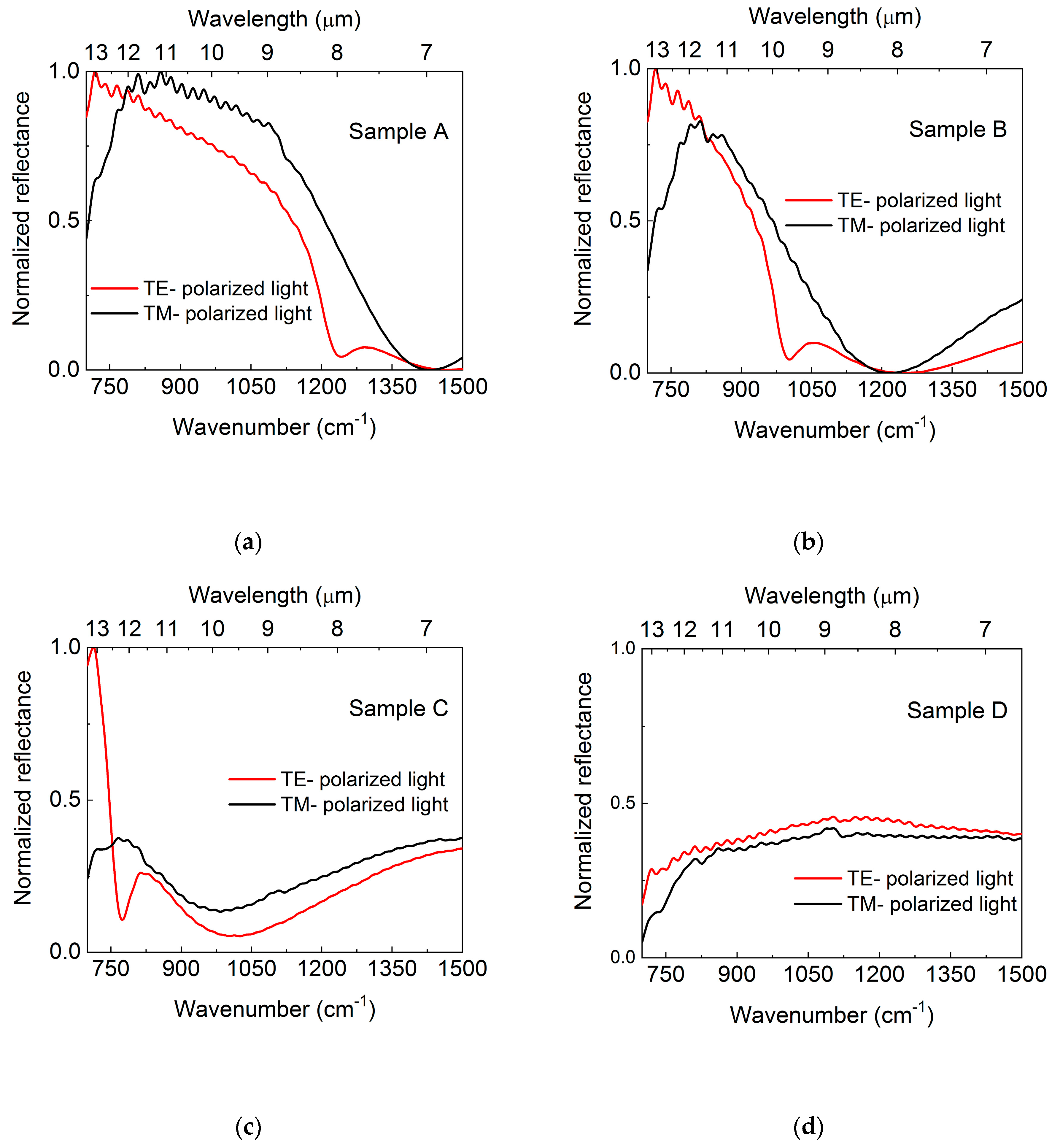
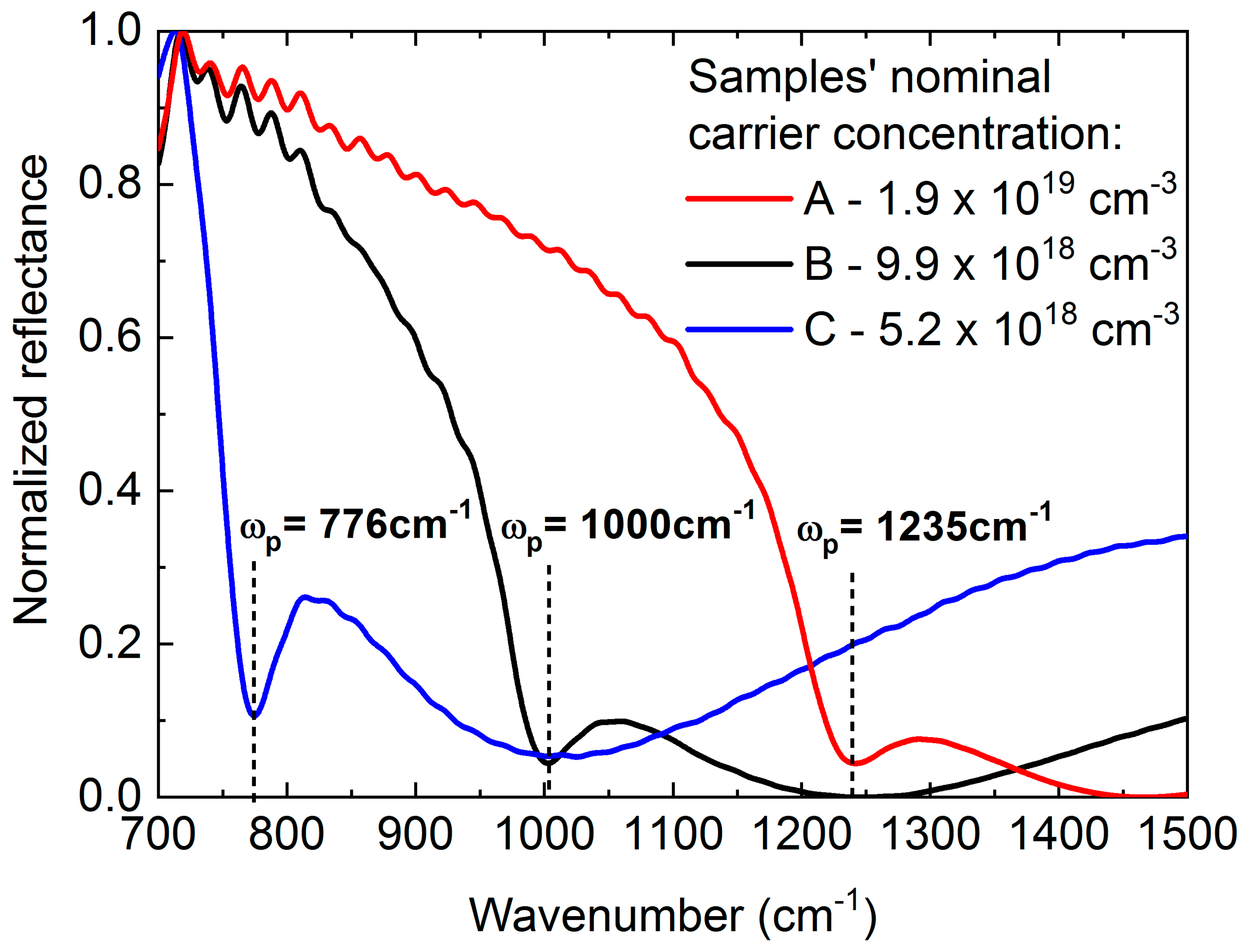
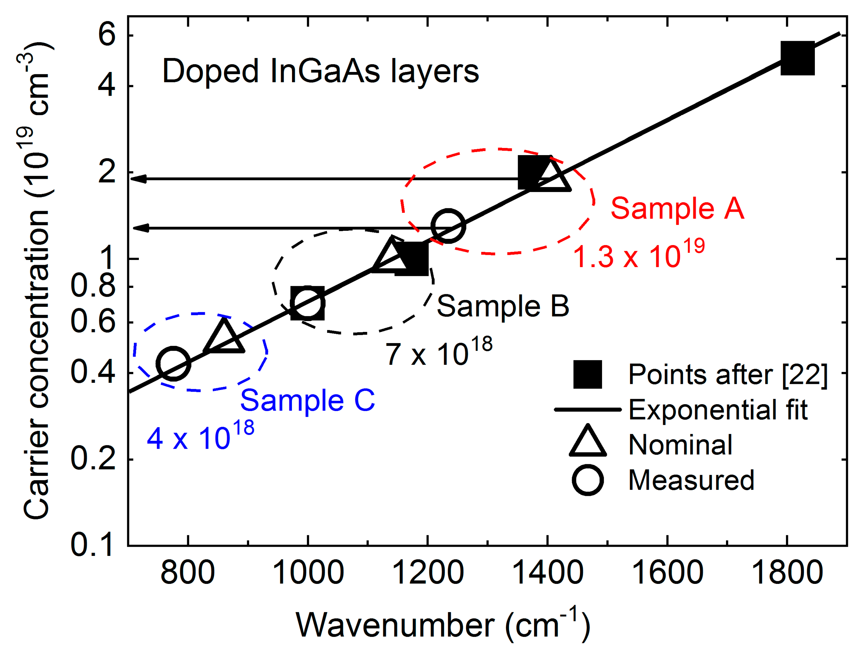
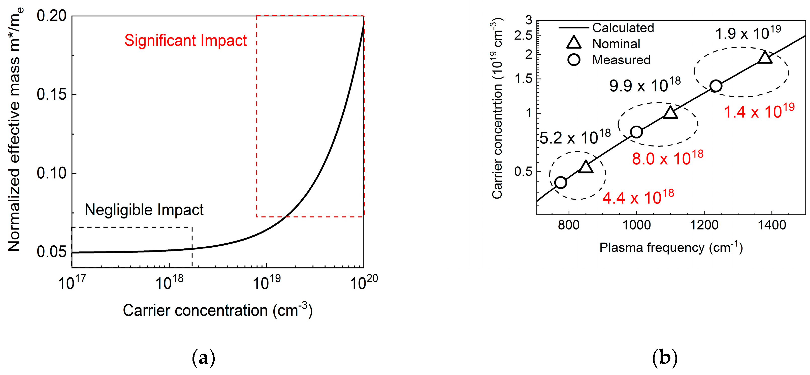
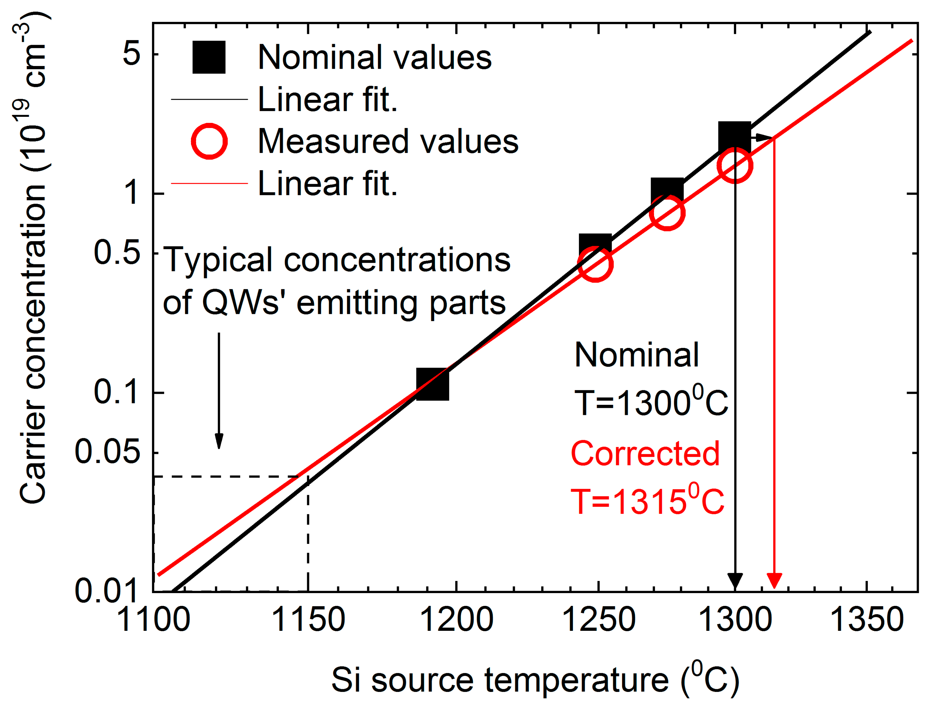
In this paper, we show the results of reflectance measurements of the Berreman effect of In0,53Ga0,47As layers samples with different nominal carrier concentrations. These are 1-µm thick Si-doped In0.53Ga0.47As layers lattice-matched to the InP substrate, grown by solid source molecular beam epitaxy (MBE) with a Riber Compact 21T reactor [21]. Different temperatures of the Si-source were used in order to vary the doping concentrations. The nominal carrier concentrations in the investigated structures were calculated by interpolation of Hall measurement curves measured with a Bio-Rad HL5500 system (Bio-rad, Hercules, CA, USA), and are shown in Table 1.
The optical measurements were performed in Bruker Vertex 80 FTIR spectrometer (Bruker, Billerica, MA, USA) with additional custom-designed evacuated external chamber to provide an oblique angle of 45 degree for the incident light [17,18] (which is necessary to observe the Berreman effect). As the light source, a glowbar was used, whereas the detector was a liquid-Nitrogen-cooled Mercury Cadmium Telluride photodiode.

3. Results

Figure 1 shows reflectance spectra for all samples measured at 300 K for two orthogonal linear polarizations of the incident light. A distinct absorption dip can clearly be seen for TM polarization (red curves), which corresponds to a case where there is an electric field component perpendicular to the sample surface. Black curves denote spectra obtained for s polarized light (TE) where there is no corresponding minimum observed, which is consistent with theory. Also visible in the red curves of the TM polarization is how the Berreman minima shift towards lower wavenumber (longer wavelength) with decreasing doping and finally even disappear for sample D due to the cut-off wavelength of our setup (detector limit at 600 cm−1).
Figure 2 shows intensity normalized reflectance spectra for the p-polarized light of three samples A, B and C. The absorption minima can be ascribed to plasma frequency ωp, of free electrons in the layers. We can see that ωp shifts to lower energies with carrier concentration decreasing according to Equation (1).
ω p 2 = n e 2 ε 0 ε m *
where ε is the material dielectric constant equal to 11.64 and ε0 is the permittivity of free space. The value of m* is 0.0453 of electron rest mass.
Figure 3 shows a comparison of the dependence of the obtained nominal carrier concentration versus plasma frequencies (black squares) obtained for InGaAs alloy with similar composition by Charache et al. [22]. This allowed us to get a useful function after exponential fitting (red line). A similar procedure has been proven to be successful when applied for the analysis of Berreman minima in the case of carrier concentration determination in InAs layers [23], using data from Hinkey et al. [24]. By open squares we marked nominal concentration values on the fitted line at the respective wavenumbers. Open solid points denote the plasmon frequencies measured by reflectivity measurements (given in wavenumbers). By placing these frequencies on the fitted curve, we were able to determine the actual electron concentrations of 1.3 × 1019 cm−3, 7.0 × 1018 cm−3, and 4.0 × 1018 cm−3 for samples A, B, and C, respectively. Furthermore, we can see that the revealed differences between the nominal and the measured concentrations, despite not being large, show for all cases the measured values to be smaller than the nominal ones. This is just the first approximation approach, which can be used as an attempt for growth parameters verification in order to establish a better match between nominal and achieved concentrations in the layers.
A more sophisticated and precise method requires including the effective mass dependence on the carrier concentration in the calculation of the plasma frequencies as a function of concentration, since it cannot be neglected for concentrations above 1018 cm−3, as in ref. [25]. Due to non-parabolic behavior of energy dispersion far from Γ point of the Brillouin zone, a correction of carrier effective mass must be taken into account, which can be expressed by Equation (2) taken from ref. [26].
m * ( n ) = m e [ 1 + 4 P 2 3 E g ( 1 + 8 P 2 2 ( 3 π 2 n ) 2 3 3 m e E g 2 ) 1 2 ] 1 ,
where me is the electron rest mass and P2 is the momentum matrix element of coupling between valence and conduction bands, calculated to be 15.4 eV.
Figure 4a shows the calculated m*/me ratio as a function of electron concentration. As we can see, the role of correction is more important for larger concentrations in the range of nominal concentrations considered within this paper (indicated by the red dotted square), where the relative changes of the effective mass up to around 30% can occur. Figure 4b shows calculated plasma frequencies assuming the mass correction (black curve) together with the nominal values (black squares) and those determined here (red circles). The obtained values are still slightly lower than nominal, however closer to the nominal values when compared to those obtained in the first, simpler approach. The respective summary is shown in Table 2. The resolution of our experimental setup was 2 cm−1, while the full widths at half maximum (FWHM) of measured spectra were ~50 cm−1. This allowed us to estimate uncertainty of the carrier concentration at ±2%, which is not enough to explain the difference between nominal concentration.

4. Discussion

Figure 5 shows the nominal electron concentrations for all investigated samples versus the applied Si source temperature together with a fit (black curve) which shows this dependence in a broader range of concentrations and temperatures. Red open circles denote determined (by second more accurate approach) electron concentrations for samples A–C together with respective fit (red curve). The comparison of the nominal dependency and the corrected experimental results shows that the respective adjustments become important for larger concentrations (higher source temperatures).
Therefore, in a range of concentrations presented in this paper, a slight temperature increase seems to be appropriate. For instance, to obtain a nominal concentration for sample A, Si source temperature should be increased by ~15 K from 1300 °C to 1315 °C to offset the observed differences. On the other hand, in the range of typical doping (~1016–1017 cm−3) of the lasing active areas of quantum cascade lasers, little temperature compensation would be required.

5. Conclusions

In this paper, we have demonstrated an optical method used for electron concentration determination in the calibration of InGaAs layers designed for waveguides of InP-based quantum cascade lasers. This method requires neither contacts nor an external magnetic field as are typically required in direct-contact methods such as Hall and C-V measurements. Moreover, the method can be applied to various types of structures, made of different kinds of materials and grown in different techniques such as metal-organic chemical vapor deposition, as well as different techniques of doping. It is important to note that 15 K is a significant difference from the point of view of manufacturing technology. There are several possible causes that would explain reported discrepancies between Hall effect method and the Berreman effect method, such as the degree of ionization of the dopant atoms in the sample, or gauging the magnetic field of the magnet, while using Hall setup. Further establishing causes of shown differences is crucial to optimize the manufacturing process and therefore the quality of ready devices due to the feasibility of the optical method, which makes it a perfect candidate to supersede other methods. By determination of the so called “Berreman effect minima” in the reflectance spectra and the derived carrier concentration versus plasma frequency, we were able to verify the nominal concentration, and finally establish Si source temperature versus concentration dependence.

Author Contributions

Conceptualization, M.M.; methodology, M.K. and M.M.; software, M.K.; validation, M.K. and M.M; formal analysis, M.K. and M.M.; investigation, M.K. and M.R.; resources, K.P. and P.G.; data curation, M.K. and M.R.; writing—original draft preparation, M.K.; writing—review and editing, M.M. and G.S.; visualization, M.K., M.R., and M.M.; supervision, M.M.; project administration, M.M.; funding acquisition, M.M. and G.S. All authors have read and agreed to the published version of the manuscript.

Funding

This work was supported by the project SENSE, founded by National Centre for Research and Development TECHMAT-STRATEG1/347510/15/NCBR/2018.

Acknowledgments

The authors would like to thank K. Ryczko for his comments and discussions regarding the performed calculations.

Conflicts of Interest

The authors declare no conflict of interest. The funders had no role in the design of the study; in the collection, analyses, or interpretation of data; in the writing of the manuscript, or in the decision to publish the results.

References

  1. Schiff, H.I.; Mackay, G.I.; Bechara, J. Air Monitoring by Spectroscopy Techniques; Wiley: New York, NY, USA, 1994. [Google Scholar]
  2. Wang, C.; Sahay, P. Breath Analysis Using Laser Spectroscopic Techniques: Breath Biomarkers, Spectral Fingerprints, and Detection Limits. Sensors 2009, 9, 8230–8262. [Google Scholar] [CrossRef] [PubMed]
  3. Airoptic. Available online: https://www.airoptic.pl (accessed on 30 January 2020).
  4. Nanoplus GmbH. Available online: https://nanoplus.com (accessed on 30 January 2020).
  5. Kosterev, A.; Wysocki, G.; Bakhirkin, Y.; So, S.; Lewicki, R.; Fraser, M.; Tittel, F.; Curl, R.F. Application of quantum cascade lasers to trace gas analysis. Appl. Phys. B 2008, 90, 165–176. [Google Scholar] [CrossRef]
  6. Nikodem, M.; Gomółka, G.; Klimczak, M.; Pysz, D.; Buczyński, R. Demonstration of mid-infrared gas sensing using an anti-resonant hollow core fiber and a quantum cascade laser. Opt. Express 2019, 27, 36350–36357. [Google Scholar] [CrossRef] [PubMed]
  7. Kluczyński, P.; Lundqvist, S.; Westberg, J.; Axner, O. Faraday rotation spectrometer with sub-second response time for detection of nitric oxide using a cw DFB quantum cascade laser at 5.33 um. Appl. Phys. B 2011, 103, 451–459. [Google Scholar] [CrossRef] [Green Version]
  8. Lu, Q.Y.; Manna, S.; Wu, D.H.; Slivken, S.; Razeghi, M. Shortwave quantum cascade laser frequency comb for multi-heterodynespectroscopy. Appl. Phys. Lett. 2018, 112, 141104. [Google Scholar] [CrossRef]
  9. Lundqvist, S.; Kluczynski, P.; Weih, R.; von Edlinger, M.; Naehle, L.; Fischer, M.; Bauer, A.; Hoefling, S.; Koeth, J. Sensing of formaldehyde using a distributed feedback interband cascade laser emitting around 3493 nm. Appl. Opt. 2012, 51, 6009–6013. [Google Scholar] [CrossRef]
  10. Tutuncu, E.; Nageke, M.; Becker, S.; Fischer, M.; Koeth, J.; Wolf, C.; Kostler, S.; Ribitsch, V.; Teuber, A.; Groeger, M.; et al. Advanced Photonic Sensors Based on Interband Cascade lasers for Real-Time Mouse Breath Analysis. ACS Sens. 2018, 3, 1743–1749. [Google Scholar] [CrossRef]
  11. Tomokage, H.; Yanahira, T.; Yoshida, M. On the Basic Assumption to Obtain Carrier Concentration Profile by Differential Hall Coefficient Measurement. Jpn. J. Appl. Phys. 1996, 35, 1824–1825. [Google Scholar] [CrossRef]
  12. Berreman, D.W. Infrared absorption at longitunal optic frequency in cubic crystal films. Phys. Rev. 1966, 130, 2193–2198. [Google Scholar] [CrossRef]
  13. Harbecke, B.; Heinz, B.; Grosse, P. Optical Properties of Thin Films and the Berreman Effect. Appl. Phys. A 1985, 38, 263–267. [Google Scholar] [CrossRef]
  14. Shaykhutdinov, T.; Furchner, A.; Rappich, J.; Hinrichs, K. Mid-infrared nanospectroscopy of Berreman mode and epsilon-near-zero local field confinement in thin films. Opt. Mater. Express 2017, 7, 3706–3714. [Google Scholar] [CrossRef]
  15. Calvani, P.; Kalaboukhov, A.; Shibayev, P.P.; Salehi, M.; Moon, J.; Oh, S.; Falsetti, E.; Ortolani, M.; Granozio, F.M.; Brubach, J.-B.; et al. Infrared spectroscopy of two-dimensional systems. Eur. Phys. J. Special Topics 2019, 228, 669–673. [Google Scholar] [CrossRef]
  16. Ibáñez, J.; Tarhan, E.; Ramdas, A.K.; Hernández, S.; Cuscó, R.; Artús, L.; Melloch, M.R.; Hopkinson, M. Direct observation of LO phonon-plasmon coupled modes in the infrared transmission spectra of n-GaAs and n-InxGa1−xAs epilayers. Phys. Rev. B 2004, 69, 075314. [Google Scholar] [CrossRef] [Green Version]
  17. Motyka, M.; Misiewicz, J. Fast Differential Reflectance Spectroscopy of Semiconductor Structures for Infrared Applications by Using Fourier Transform Spectrometer. Appl. Phys. Express 2010, 3, 112401. [Google Scholar] [CrossRef]
  18. Motyka, M.; Sek, G.; Janiak, F.; Misiewicz, J.; Klos, K.; Piotrowski, J. Fourier-transformed photoreflectance and fast differential reflectance of HgCdTe layers. The issues of spectral resoultion and Fabry-Perot oscillations. Meas. Sci. Technol. 2011, 22, 125601. [Google Scholar] [CrossRef]
  19. Motyka, M.; Sęk, G.; Misiewicz, J.; Bauer, A.; Dallner, M.; Höfling, S.; Forchel, A. Fourier Transformed Photoreflectance and Photoluminescence of Mid infrared GaSb-Based Type II Quantum Wells. Appl. Phys. Express 2009, 2, 126505. [Google Scholar] [CrossRef]
  20. Dyksik, M.; Motyka, M.; Kurka, M.; Ryczko, K.; Schade, A.; Kamp, M.; Höfling, S.; Sęk, G. Electrical Tuning of the oscillator strength in type II InAs/GaInSb quantum wells for active regions of passively mode-locked interband cascade lasers. Jpn. J. Appl. Phys 2017, 56, 110301. [Google Scholar] [CrossRef] [Green Version]
  21. Gutowski, P.; Sankowska, I.; Karbownik, P.; Pierscinska, D.; Serebrennikova, O.; Morawiec, M.; Pruszynska-Karbownik, E.; Golaszewska-Malec, K.; Pierscinski, K.; Muszalski, J.; et al. MBE growth of strain-compensated InGaAs/InAlAs/InP quantum cascade lasers. J. Cryst. Growth 2017, 466, 22–29. [Google Scholar] [CrossRef]
  22. Charache, G.; DePoy, D.; Raynolds, J.; Baldasaro, P.; Miyano, K.; Holden, T.; Pollak, F.; Sharps, P.; Timmons, M.; Geller, C.; et al. Moss-Burstein and plasma reflection characteristics of heavily doped n-type InxGa1-xAs and InPyAs1-y. J. Appl. Phys. 1999, 86, 242452. [Google Scholar] [CrossRef]
  23. Kozub, M.; Motyka, M.; Dyksik, M.; Sek, G.; Misiewicz, J.; Nishisaka, K.; Maemoto, T.; Sasa, S. Non-destructive carrier concentration determination in InAs thin films for THz radiation generating devices using fast differential reflectance spectroscopy. Opt. Quant. Electron. 2016, 48, 384. [Google Scholar] [CrossRef] [Green Version]
  24. Hinkey, R.; Tian, Z.; Yang, R.; Mishima, T.; Santos, M. Reflectance spectrum of plasmon waveguide interband cascade lasers and observation of the Berreman effect. J. Appl. Phys. 2011, 110, 043113. [Google Scholar] [CrossRef]
  25. Dyksik, M.; Motyka, M.; Sek, G.; Misiewicz, J.; Dallner, M.; Höfling, S.; Kamp, M. Influence of carrier concentration on properties of InAs waveguide layers in interband cascade laser structures. J. Appl. Phys. 2016, 120, 043104. [Google Scholar] [CrossRef] [Green Version]
  26. Li, Y.; Stradling, R.; Knight, T.; Birch, J.; Thomas, R.; Phillips, C.; Ferguson, I. Infrared reflection and transmission of undoped and Si-doped InAs grown on GaAs by molecular beam epitaxy. Semicond. Sci. Technol. 1993, 8, 101. [Google Scholar] [CrossRef]
Figure 1. The reflectance spectra for two orthogonal polarizations of the probing light denoted TE (red curves) and TM (black curves): (a) 1.9 × 1019 cm−3; (b) 9.9 × 1018 cm−3; (c) 5.2 × 1018 cm−3; (d) 1.1 × 1018 cm−3.
Materials 13 03109 g001
Figure 2. Normalized p-polarized reflectance spectra for Sample A (red curve), Sample B (black curve), and Sample C (blue curve) together with given characteristic reflectance minima at plasma frequencies and indication of carrier nominal concentration.
Materials 13 03109 g002
Figure 3. Carrier concentration in a function of Plasma frequency. Black squares denotes points after ref. [22] together with respective fit (red line). Triangular points represents nominal concentrations and open circles those established.
Materials 13 03109 g003
Figure 4. (a) Electron mass changes as a function of their concentration after Equation (2); (b) Plasma frequencies as a function of electron concentration. Black curve represents calculated Plasma frequencies assuming mass correction shown in panel (a). Open triangles depicts nominal values and open circles those measured.
Materials 13 03109 g004
Figure 5. Nominal carrier concentrations (black squares) as a function of applied Si source temperature together with fit (black curve). Open red circles denotes corrected (in the way of second approach) values of the carrier concentration in a function of the applied Si source temperature together with respective fit (red curve).
Materials 13 03109 g005
Table 1. The samples’ description.
SampleHall-Measured Carrier Concentration (cm−3)Si-Source Nominal Temperature (°C)
(A) C7661.9 × 10191300
(B) C7649.9 × 10181275
(C) C763 5.2 × 10181250
(D) C7591.1 × 10181190
Table 2. The samples’ description and growth protocol.
SampleNominal Carrier ConcentrationFirst ApproachSecond Approach
(A) C7661.9 × 10191.3 × 10191.38 × 1019
(B) C7649.9 × 10187.0 × 10188.0 × 1018
(C) C763 5.2 × 10184.0 × 10184.4 × 1018
(D) C7591.1 × 1018N/AN/A

