Communication

Photoluminescence Characteristics of Sn2+ and Ce3+-Doped Cs2SnCl6 Double-Perovskite Crystals

Key Laboratory for Ultrafine Materials of Ministry of Education, School of Materials Science and Engineering, East China University of Science and Technology, Shanghai 200237, China
*
Author to whom correspondence should be addressed.
Materials 2019, 12(9), 1501; https://doi.org/10.3390/ma12091501
Submission received: 18 April 2019 / Revised: 5 May 2019 / Accepted: 6 May 2019 / Published: 8 May 2019
(This article belongs to the Section Optical and Photonic Materials)

Abstract

:
In recent years, all-inorganic lead-halide perovskites have received extensive attention due to their many advantages, but their poor stability and high toxicity are two major problems. In this paper, a low toxicity and stable Cs2SnCl6 double perovskite crystals were prepared by aqueous phase precipitation method using SnCl2 as precursor. By the XRD, ICP-AES, XPS, photoluminescence and absorption spectra, the fluorescence decay curve, the structure and photoluminescence characteristics of Ce3+-doped and undoped samples have been investigated in detail. The results show that the photoluminescence originates from defects. [ S n S n 4 + 2 + +VCl] defect complex in the crystal is formed by Sn2+ substituting Sn4+. The number of defects formed by Sn2+ in the crystal decreases with Ce3+ content increases. Within a certain number of defects, the crystal luminescence is enhanced with the number of [ S n S n 4 + 2 + +VCl] decreased. When Ce3+ is incorporated into the crystals, the defects of [ C e 3 + S n 4 + +VCl] and [ S n S n 4 + 2 + +VCl] were formed and the crystal show the strongest emission. This provides a route to enhance the photoluminescence of Cs2SnCl6 double perovskite crystals.

1. Introduction

In recent years, the excellent performance of lead halide perovskite in optical instruments has attracted increasing attention in the professional sphere [1]. Since the Mitzi research group [2] first reported organic-inorganic hybrid perovskite material and found its strong electron migration capability at the end of the 20th century. The great potential of applying its capability to solar cells has inspired a new wave of research at the time [3,4,5]. Using the liquid phase method, the researchers synthesized all inorganic lead-halide perovskite CsPbX3 (X = Cl,Br,I) nanocrystal [6,7], which has the same structure as hybrid perovskite [8]. The synthesized nanocrystals have captured much attention with their superior features, including high fluorescence quantum efficiency (up to 100%) [9], light emission wavelength covering the entire visible spectrum (400–700 nm) [10], relatively narrow full width at half maximum (FWHM) (12–42 nm) [11] etc. Therefore, they have shown a great application potential in the light emitting diode (LED) [12,13], quantum dot light emitting diodes (QLED) [14], laser [15,16], fluorescent probe [17] and the energy conversion efficiency of CH3NH3PbI3 and CsPbI3 solar cells has reached 23% [18]. Although CH3NH3PbX3 and CsPbX3 exhibit excellent performance, there still remains a major concern on its application, namely the high toxicity of lead [19]. If the lead is always included in the solar photovoltaic module, it will not cause any problems. However, the fact that lead-based perovskite would normally release PbX2 as a degradation product, which would cause negative effects on health and the environment [20]. The global demand for renewable and green energy has triggered the exploration of low-cost, high-efficiency photovoltaic device. In order to realize a wider application of perovskite device, replacing the unsafe lead component seems to be vital. The tin-based perovskite CsSnX3 is a very good substitute for applications in solar cells, infrared light-emitting diodes and lasers [21,22,23,24,25]. Unfortunately, the Sn2+ in CsSnX3 perovskites is easily oxidized to Sn4+, resulting in high sensitivity to ambient atmospheres (oxygen, moisture, etc.) [21,22,26,27].
As a defect variant of the traditional cubic ABX3 perovskite, Cs2SnX6 has a crystal structure similar to that of CsPbX3. Cs2SnX6 is expected to be applied to large-scale production [28] since it has considerable stability to oxygen and moisture. The high stability is attributed to the high value Sn4+ and higher decomposition enthalpy (1.37 eV per formula unit for Cs2SnCl6) than that of traditional ABX3 halide perovskites (e.g., 0.29 eV for CsPbBr3) [29]. Many publications have reported recently the preparation method and potential applications of Cs2SnX6 perovskite crystals. Among those, Wang A et al. [1] synthesized Cs2SnI6 nanocrystals and proved that the Cs2SnX6 based field effect transistor has the characteristics of a P-type semiconductor with high hole mobility (>20 cm2/(Vs)). Kaltzoglou A et al. synthesized Cs2SnCl6,Cs2SnBr6,Cs2SnI6 and Cs2SnI3Br3 crystals under different temperatures using different solvents [28,30]. These crystals were used as hole transport materials in dye-sensitized solar cells, its power conversion efficiency has reached maximum 4.23% under one solar radiation. At meanwhile, Saparov B et al. [19] obtained an n-type Cs2SnI6 semiconductor film by annealing SnI4 vapor onto a glass substrate covered with a CsI film. Xiaofeng Qiu et al. [22] oxidized CsSnI3 film into Cs2SnI6 film as the light absorbing layer in solar cells.
Nevertheless, there are very few reports on the luminescence properties of the Cs2SnCl6 crystal, except the recent one about strong blue light emitting by doping Bi3+ [29]. Actually, a few Sn2+ ions play a key role in producing BiSn+VCl defect complex, which is responsible for the strong blue emission according to the literature [29]. It is unclear whether Sn2+ itself or the other trivalent ions have similar behavior. Therefore, in this paper, SnCl2 and CsCl are used as precursors to synthesize Cs2SnCl6 crystals by liquid phase precipitation method. The blue light-emitting crystals in which defect band reduce the original band gap in the forbidden band were obtained by doping and the effects of Sn2+ and Ce3+ on the luminescence properties of the crystal have been investigated.

2. Materials and Methods

2.1. Chemicals

Tin (Sn, 99.9%, Aladdin, Shanghai, China), cesium chloride (CsCl, 99.99%, Aladdin, Shanghai, China), cerium chloride heptahydrate (CeCl3·7H2O, 99.99%, Henghua, Ninan, China), hydrochloric acid (HCl, 36–38%, Titan, Shanghai, China), deionized water (H2O), absolute alcohol (C2H6O, Titan, Shanghai, China).

2.2. Preparation of SnCl2 Solution

The Sn powder and HCl were taken in a beaker at a molar ratio of 1:4 and the beaker was heated at 90 °C for ensuring complete dissolution of tin powder to prepare SnCl2 solution. Since Sn2+ easily was oxidized to Sn4+ under certain conditions, leading to the solution containing SnCl2 and SnCl4 (for convenience, it was also represented by SnCl2 hereinafter).

2.3. Synthesis of Cs2SnCl6 Crystals

The beaker containing 0.036 mol CsCl, 60 mL concentrated hydrochloric acid and 78 mL deionized water was heated to 90 °C in a water bath. 0.018 mol of newly synthesized SnCl2 was injected by a pipette with stirring. 1/6 samples were taken out at different time point (0 min, 10 min, 60 min, 360 min, 660 min, 1020 min). The samples were naturally cooled to room temperature and centrifuged to obtain a precipitate, which was washed twice with absolute ethanol to remove hydrochloric acid on the surface of the samples and naturally dried in the air. The samples have been numbered as A1–A6 in Table 1.

2.4. Synthesis of Ce3+-Doped Cs2SnCl6 Crystals

Firstly, the beaker containing a certain amount of CsCl, different amount of CeCl3·7H2O, 10 mL concentrated hydrochloric acid and 13 mL deionized water was heated to 90 °C and then 0.003 mol of SnCl2 was injected by a pipette. Secondly, the mixture has reacted for 11 h at 90 °C and then naturally cooled to room temperature and centrifuged to obtain precipitate. Finally, the samples were washed twice with absolute ethanol to remove hydrochloric acid and Ce3+ on the surface of the samples and naturally dried in the air. The samples have been numbered as C1–C5 in Table 1.
The same preparation steps have been employed to investigate the effect of different reaction time for Ce3+-doped Cs2SnCl6 samples by adding 3-fold amount of CsCl, concentrated hydrochloric acid, deionized water and SnCl2 to the beaker, 1/3 volume of solution was taken for measurements. The samples have been numbered as B1–B3 in Table 1.

2.5. Measurements

The chemical states of Cs, Sn, Ce and Cl were determined by X-ray photoelectron spectroscopy (XPS, ESCALAB 250Xi, Thermo Fisher, Basingstoke, UK). The XRD patterns of the sample were measured by an X-ray diffractometer (D/MAX 2550 VB/PC, Rigaku Corporation, Tokyo, Japan). The doping concentration of Ce3+ was determined by inductively coupled plasma optical emission spectrometry (ICP-AES, Agilent, Santa Clara, CA, USA). The reflectance and fluorescence spectra of the samples were measured by an UV-visible spectrophotometer (UV-2550, Shimadzu, Kyoto, Japan) and a molecular fluorescence spectrometer (Fluorolog-3-P, Jobin Yvon, Paris, France). The fluorescence quantum efficiency and fluorescence lifetime of the Cs2SnCl6: Ce were determined by a fluorescence spectrometer with an integrating sphere (FLS980, Edinburgh instrument Ltd., Livingston, UK).

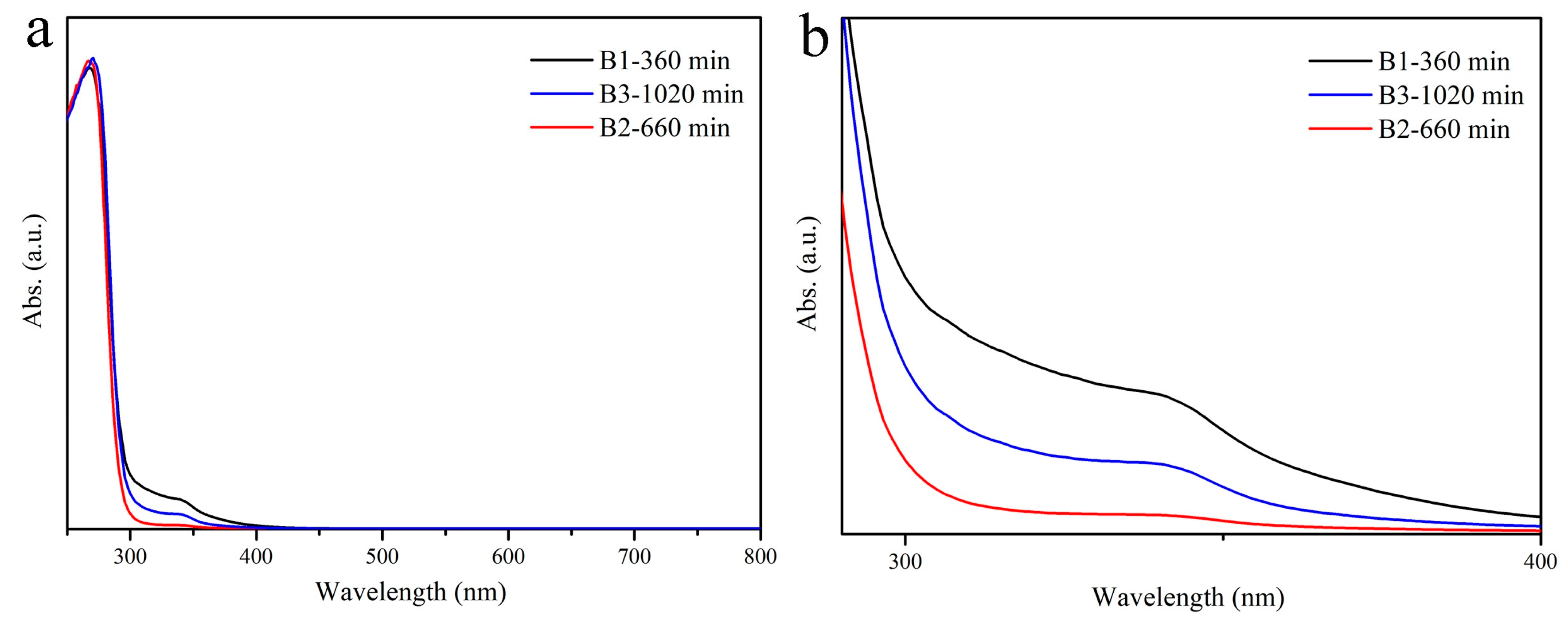
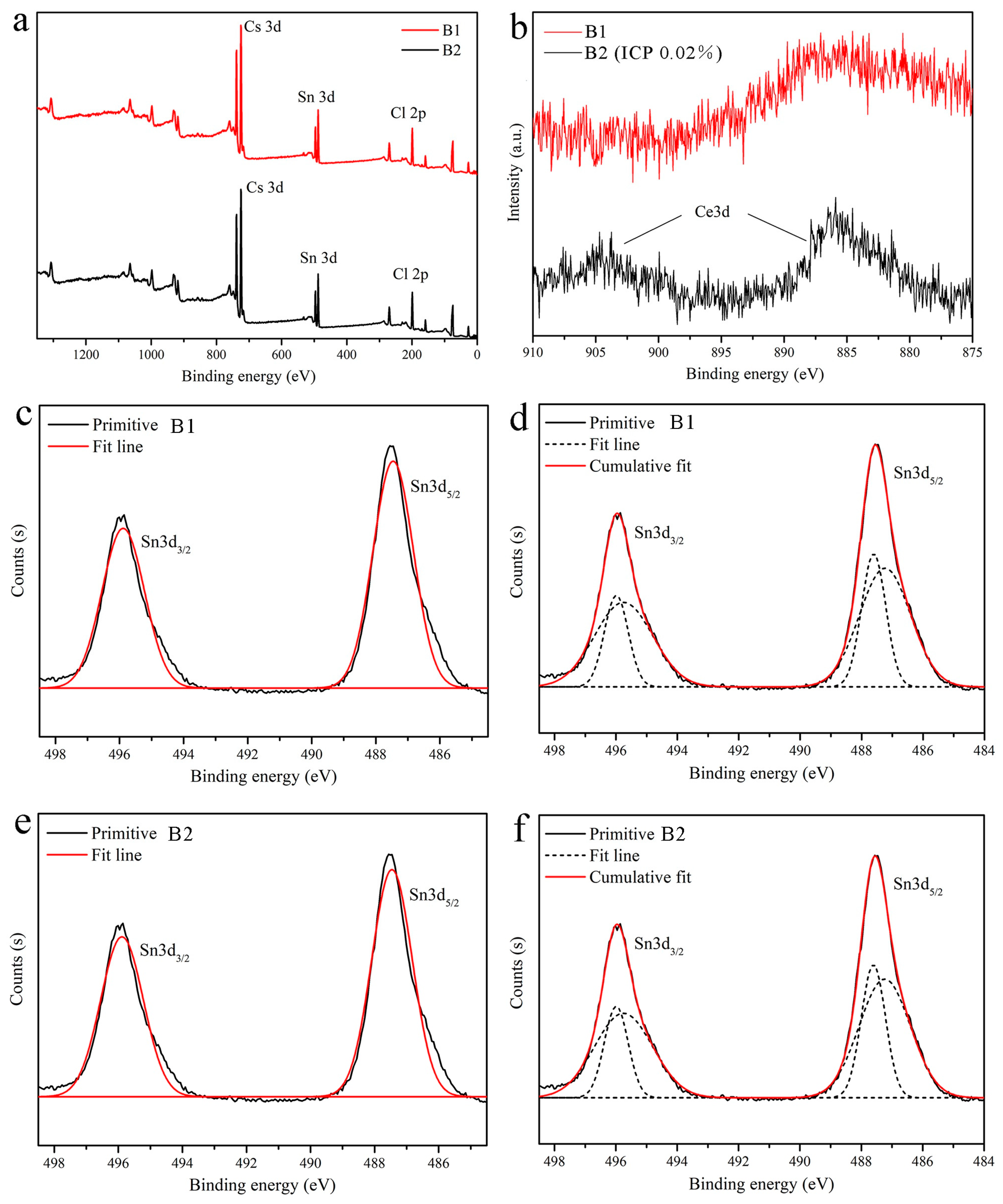
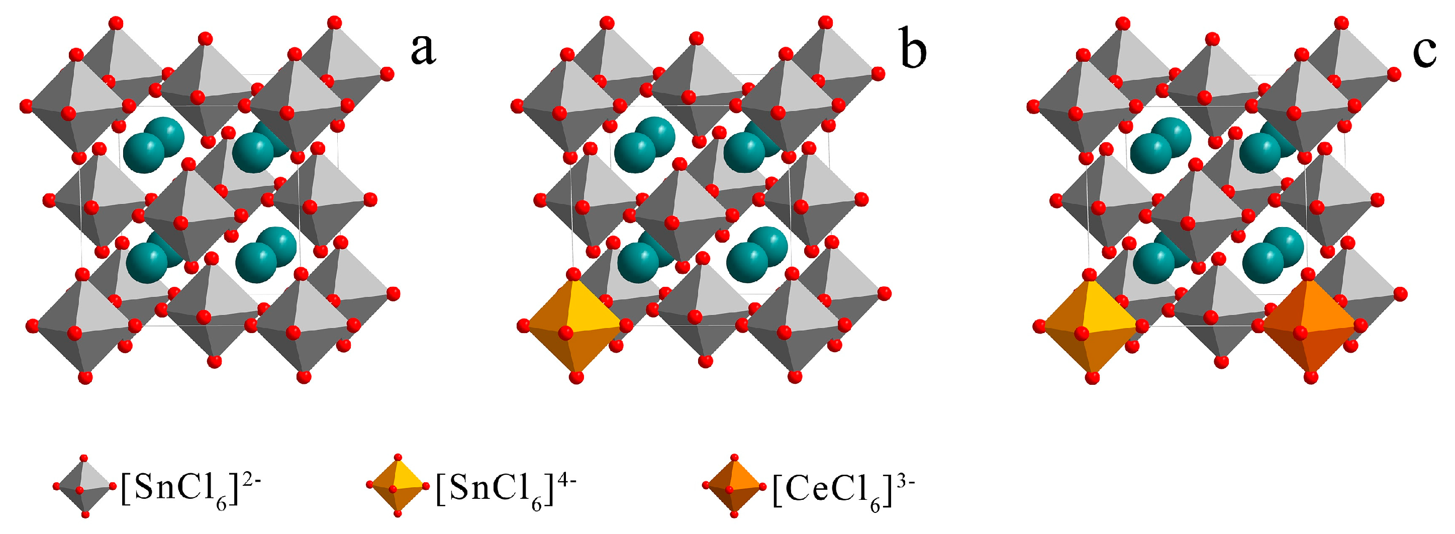
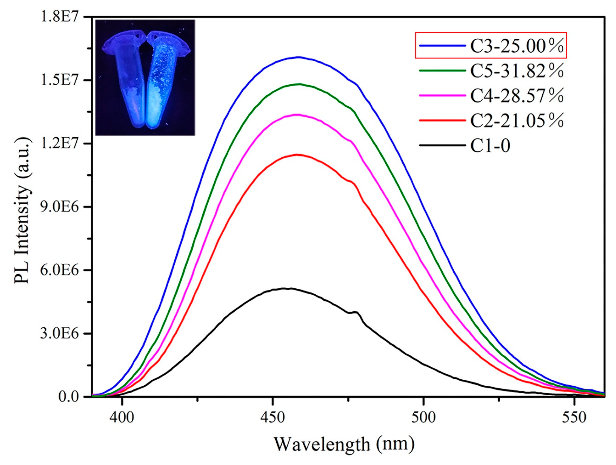
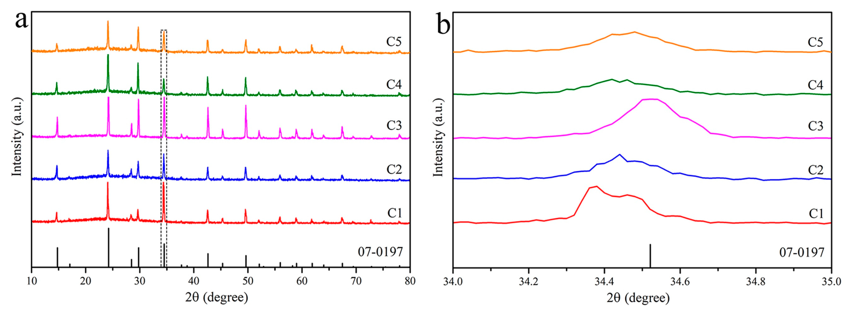
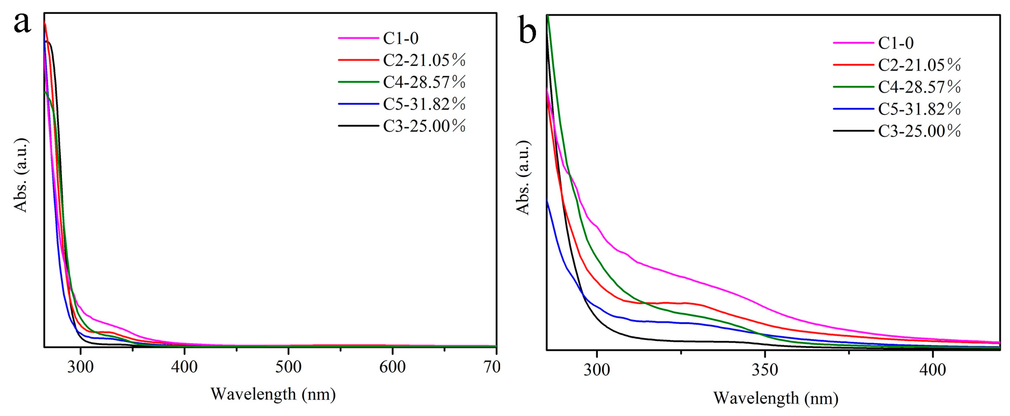
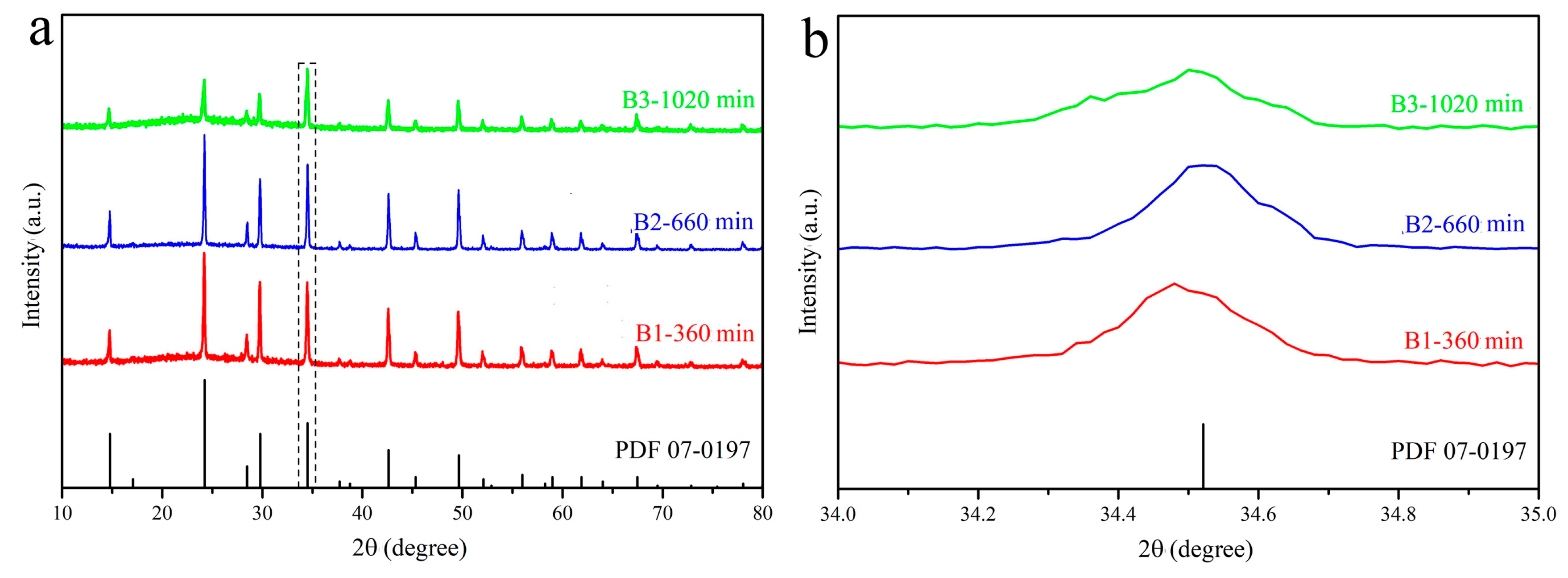
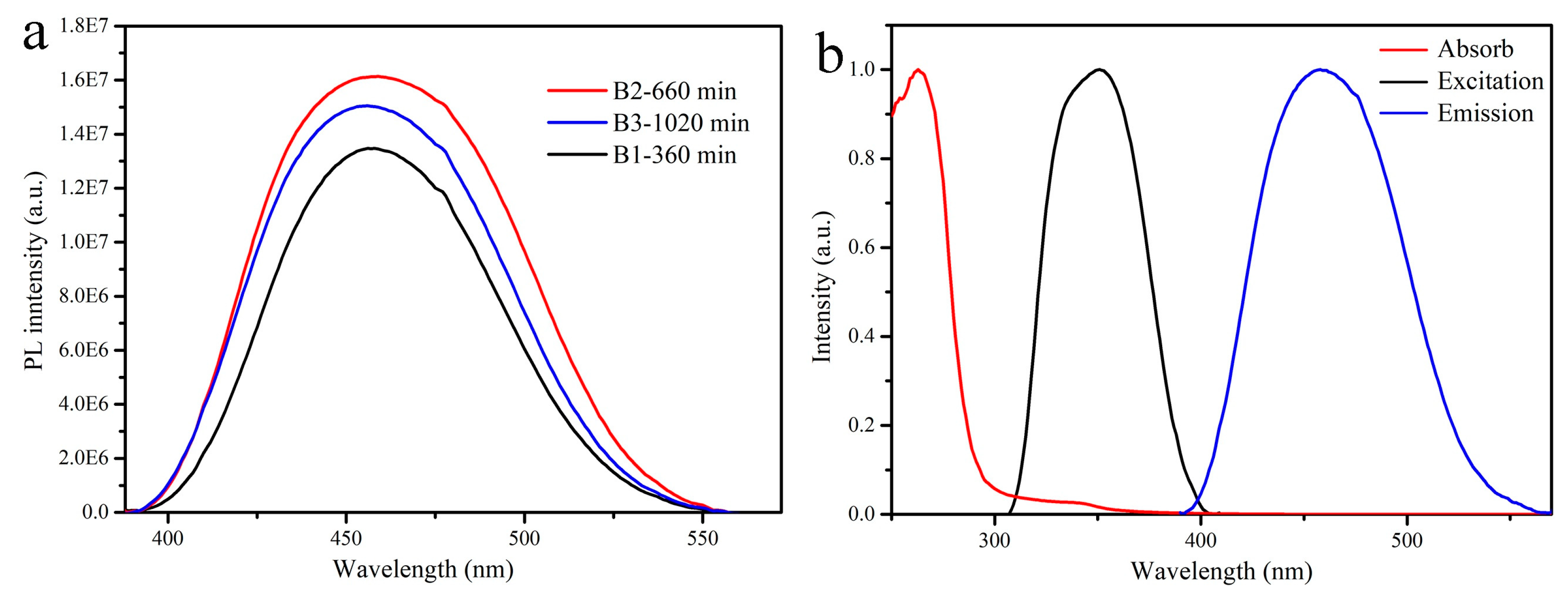
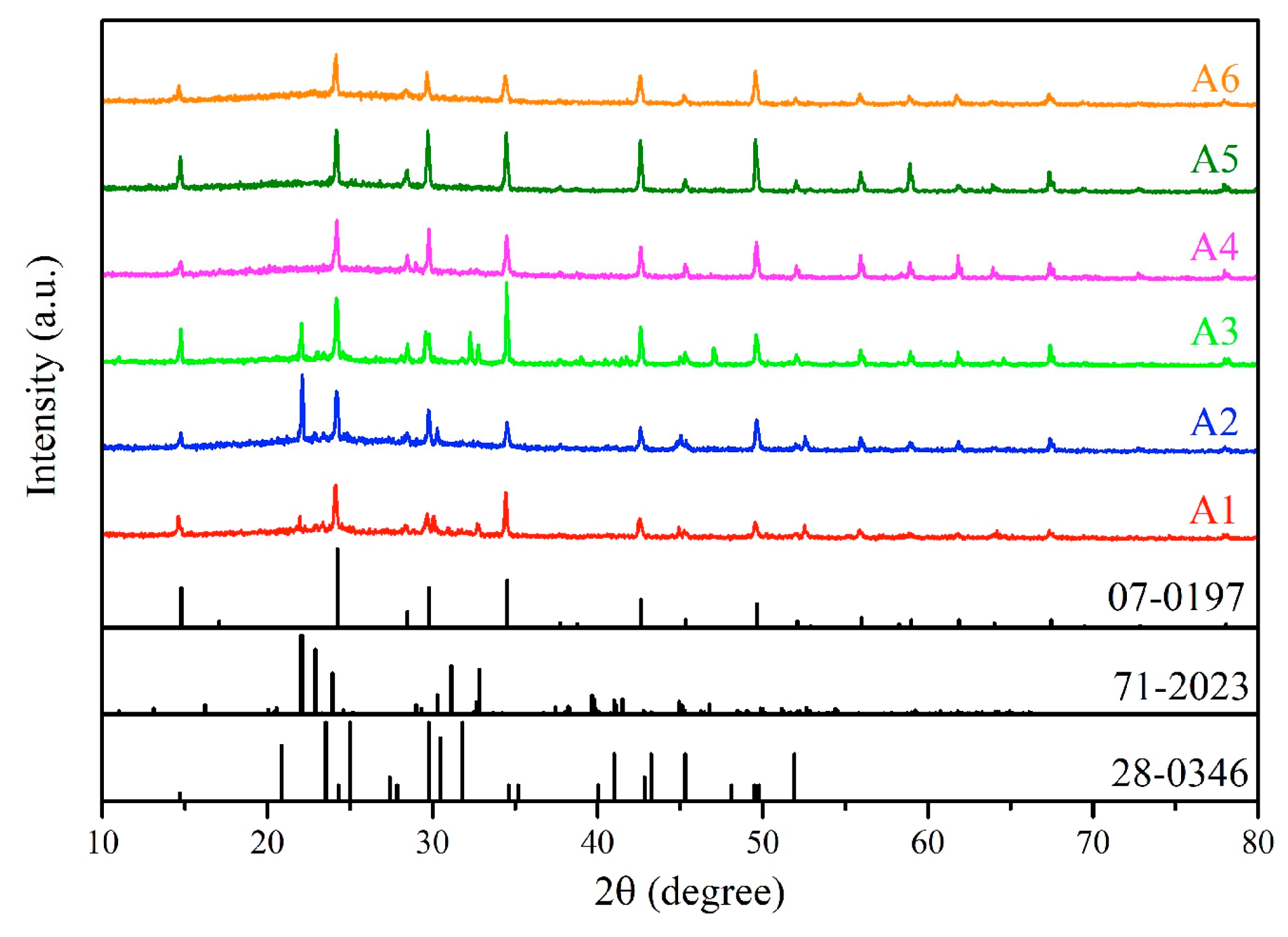
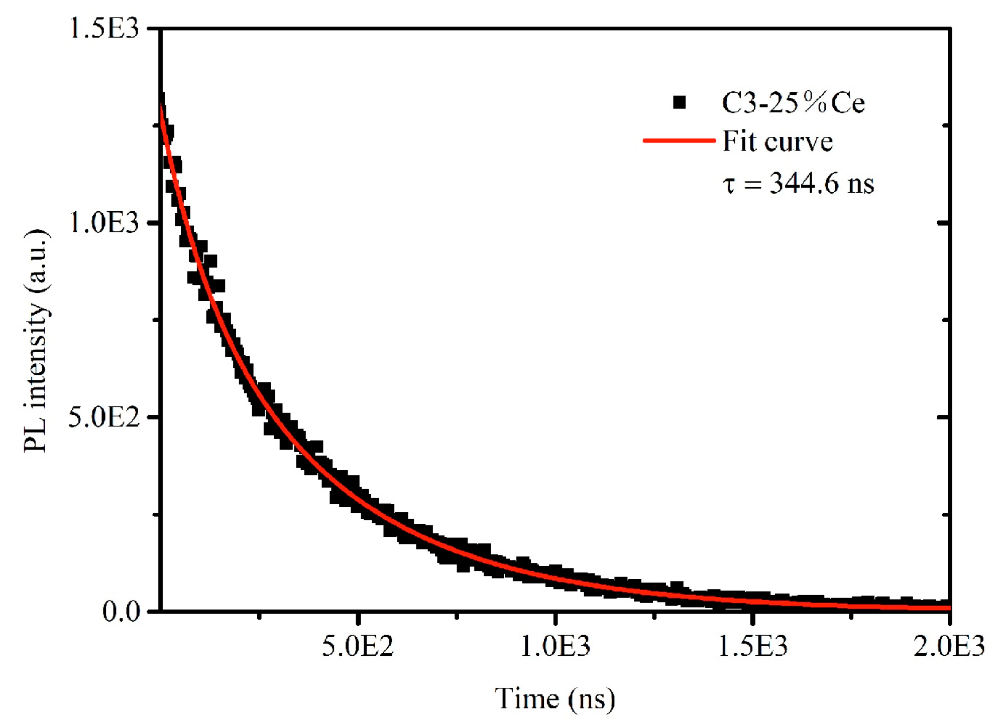
3. Results and Discussion

The absorption spectra of 25% Ce3+-doped Cs2SnCl6 crystals at different reaction time are shown in Figure 1. All samples have shown a same strong absorption band with an edge (Figure 1b) at 312 nm (3.97 eV), which is consistent with the absorption edge reported in the literature at 317 nm (3.9 eV) [28] and 313 nm (3.96 eV) [31], indicating this absorption band originates from the absorption of the Cs2SnCl6 matrix. In addition to the absorption of the matrix, the absorption spectra have exhibited an extra weak absorption band between 312 and 390 nm. The similar weak absorption band has also been exhibited when doping Bi3+ in the literature [29]. In this literature, it figured out that the formation of [VCl+BiSn] defect complex by introducing Bi3+ creates a defect energy band composed of Cl 3p and Bi 6s orbitals above the valence band maximum (VBM), resulting in the additional absorption band. Therefore, it is reasonable to infer that the extra weak absorption band in the absorption spectra in this work is similar to the literature [29], but which might be caused by the defect formed by Ce3+ or Sn2+ doping because of the absence of Bi3+. the absorption intensity increases as the number of defects increases. The intensities of the weak absorption bands increase in the order of B2, B3 and B1, which means contrary defect concentration order due to the positive correlation between the absorption intensity and the defect concentration.
To further demonstrate the above inference, the measured ICP-AES data of the samples were also listed in Table 1. Only the B2 sample contained a few of Ce3+ with a mass of 0.02% among three samples. Figure 2 has shown the XPS spectra of B1 and B2 and the fitted spectra of high-resolution Sn 3d. Only the energy peaks of Cs, Sn and Cl appeared in the total spectra. The Sn 3d spectra composed of two asymmetrical peaks at about 496 eV and 487 eV respectively. To clarify the origin of two peaks, they were fitted by using Sn4+ (Figure 2c,e) and Sn4+/Sn2+ pair (Figure 2d,f), as a result the later exhibited better fitting degree. It suggests the existence of the characteristics 3d3/2 (495.7 eV) and 3d5/2 (487.2 eV) peaks of Sn2+ in addition to Sn4+ 3d3/2 (496.1 eV) and 3d5/2 (487.6 eV) [29,32]. Furthermore, comparing the Ce 3d high-resolution spectra of B1 and B2, two weak Ce3+ in the range of 879–890 eV and 900–910 eV [24] peaks for B2 can be seen but none for B1, which is consistent with the ICP-AES results. Therefore, the impurities in the B1 and B3 are Sn2+, while the B2 contains Sn2+ and Ce3+.
Figure 3 is the XRD patterns of the samples B1–B3. All samples are Cs2SnCl6 crystal phase with the Fm-3m space group. No impurities’ peaks appeared after the addition of Ce3+. Their diffraction peaks shift to smaller angle by comparison with the standard card, as seen from Figure 3b, due to the substitution of Sn4+ (r = 0.069 nm) by a larger ion radius of Sn2+ (r = 0.112 nm) or Ce3+ (r = 0.102 nm). Among three samples, the smallest shift for B2 sample could be attributed to the fact that only B2 has Ce3+ from the results of ICP-AES and XPS.
The photoluminescence (PL) spectra of the B1–B3 were plotted in Figure 4. All samples have shown the same broad emission band peaking at 455 nm with a full width at half maximum (FWHM) of 80 nm under 350 nm illumination, according with the broadband emission spectrum peaking at 454 nm in the literature [29]. It suggests that the luminescence of the samples in this work could also originate from a similar defect to the literature [29]. By comparing the defect concentration order, the PL intensity gradually contrarily decreases in the order of B2, B3 and B1 (Figure 4a), suggesting that the PL intensity decreases as increasing defect concentration. The higher defect concentration is easier to form defect clusters, resulting in serious self-absorption, which weakens the luminescence [29]. Therefore, the oxidization of Sn2+ in the precursor and crystal to Sn4+ possibly causes the concentration of defects decreases as increasing the reaction time. To prove the oxidation process, the new synthesized SnCl2 solution was employed as the precursor to synthesize the A-series samples without Ce3+ doping. Their XRD patterns were shown in Figure 5. The samples with the reaction time below 60 min composed of Cs2SnCl4 (PDF#28-0346) and CsSnCl3 (PDF#71-2023). Besides, the diffraction peaks of CsSnCl3 (PDF#71-2023) crystal existed in 360 min sample. Pure phase Cs2SnCl6 crystals were obtained as the reaction time prolonged to 660 and 1020 min. A larger amount of Sn2+ existed in the new synthesized SnCl2 solution since the amount of Sn2+ oxidized to Sn4+ is relatively smaller, so that the Cs2SnCl6 crystals together with Cs2SnCl4 and CsSnCl3 were formed at the beginning of the reaction. However, Cs2SnCl4 and CsSnCl3 were gradually oxidized to Cs2SnCl6 as the reaction time prolonged and finally pure phase Cs2SnCl6 crystals were obtained.
The crystal structure schematic diagrams of the doped Cs2SnCl6 were shown in Figure 6. Although the B-series samples contain different types of impurities, their PL and absorption spectra are consistent in peak position and shape, indicating the same type of defects, that is, the composite defects formed by the substitution of Sn4+ and Cl vacancies, namely the sample B2 contains [ C e 3 + S n 4 +   +VCl] and [ S n S n 4 + 2 + +VCl] and only [ S n S n 4 + 2 + +VCl] exists in B1 and B3.
Figure 7 is the PL spectra of Ce-doped samples at different concentrations. The undoped sample C1 show very low PL intensity. The intensity was enhanced with increasing the doping concentration and the C3 sample containing Ce3+ (listed in Table 1) had the highest intensity. The measured fluorescence quantum efficiency of the C3 sample was 6.54% and the blue light can be observed under ultraviolet light irradiation (shown in the inset of Figure 7). Although the efficiency is much lower than that of Bi3+ doped samples [29], as our best knowledge, this is the first report about the PL of the Cs2SnCl6 crystal.
The PL decay curve of the sample C3 was measured and fitted by the Equation (1), as shown in Figure 8.
I   =   A   e x p   ( t / τ )
I represents the PL intensity of the sample as a function of time, A is a constant, t is time and τ is the fluorescence lifetime of the sample. The fluorescence lifetime τ of the C3 sample is 344.6 ns. This is much higher than that of Ce3+, such as 25 ns for BaBPO5:Ce, 70 ns for Y3A15O12:Ce [33,34]. It is also much lower than the fluorescence lifetime (5 µs) of the Sn2+ dopant luminescent material [35]. These suggested that the PL of the Cs2SnCl6 crystals in this paper is not derived from Sn2+ and Ce3+ themselves but the defects formed by them.
The XRD patterns shown in Figure 9 show that the shift degree of the diffraction peaks decreases with the order of C1, C2, C4 and C5. Meanwhile, comparing with the absorption spectra shown in Figure 10, the intensity of the additional weak absorption band decreased gradually. Therefore, it inferred that the concentration of the defects formed by Sn2+ reduced gradually because these samples only contained the Sn2+ impurity. Although Ce3+ was not incorporated into all samples as expected, the addition of Ce3+ could impair the content of Sn2+ in the crystals as well as the PL intensity. It is presumed that the probability of Sn2+ entering the crystal lattice could be reduced with increasing the introduction amount of Ce3+, so that the defects caused by Sn2+ in the crystals have been reduced. When Ce3+ entered the crystal lattice, the total number of defects has been reduced, leading to the PL enhancement within a certain concentration range of the defects. However, the reason of Sn2+ defects affected by Ce3+ need to be further investigated. Furthermore, only the C3 sample contained Ce3+, suggesting the difficulty to introduce Ce3+ in this crystal, which can be related to ionic radius and electronegativity [36,37]. The ionic radius of Ce3+ (r = 0.102 nm) is quite different from that of Sn4+(r = 0.069 nm) and the electronegativity (1.7) of Sn2+ is closer to 1.9 of Sn4+ [38], compared with the Ce3+ (1.2). Therefore, Sn2+ could be more likely to replace Sn4+ into the crystal. Another reason is that the Sn2+ was used as the precursor to enter the crystal together with Sn4+.

4. Conclusions

The SnCl2 solution was used as the precursor and Ce3+ was doped to synthesize Cs2SnCl6 crystals. The undoped and Ce3+-doped Cs2SnCl6 crystals have similar emission spectra peaking at 455 nm with a FWHM of 80 nm. By doping Ce3+, the PL intensity was enhanced remarkably. The luminescence of the crystals is derived from the defects introduced by Sn2+. When only Sn2+ impurities are present in the crystal, [ S n S n 4 + 2 + +VCl] defects are formed. In the range of a certain number of defects, the crystal PL intensity increases with the number of defects. When the crystals contain Sn2+ and Ce3+ impurities, in which the [ S n S n 4 + 2 + +VCl] and [ C e 3 + S n 4 +   +VCl] defects are formed, the emission of the crystals is the strongest and the fluorescence quantum efficiency is 6.54% with fluorescence lifetime 344.6 ns.

Author Contributions

Investigation, H.Z. and L.Z.; Resource, J.C., L.C. and C.L.; Writing—Original Draft Preparation, H.Z.; Writing—Review & Editing, S.Y.

Funding

This research received no external funding.

Conflicts of Interest

The authors declare no conflict interest.

References

  1. Wang, A.; Yan, X.; Zhang, M.; Sun, S.; Yang, M.; Shen, W.; Pan, X.; Wang, P.; Deng, Z. Controlled Synthesis of Lead-Free and Stable Perovskite Derivative Cs2SnI6 Nanocrystals via a Facile Hot-Injection Process. Chem. Mater. 2016, 28, 8132–8140. [Google Scholar] [CrossRef]
  2. Kagan, C.R.; Mitzi, D.B.; Dimitrakopoulos, C.D. Organic-inorganic Hybrid Materials as Semiconducting Channels in Thin-film Field-effect Transistors. Science 1999, 286, 945–947. [Google Scholar] [CrossRef] [PubMed]
  3. Talapin, D.V.; Lee, J.S.; Kovalenko, M.V. Prospects of colloidal nanocrystals for electronic and optoelectronic applications. Chem. Rev. 2010, 110, 389–458. [Google Scholar] [CrossRef] [PubMed]
  4. Beal, R.E.; Slotcavage, D.J.; Leijtens, T. Cesium Lead Halide Perovskites with Improved Stability for Tandem Solar Cells. J. Phys. Chem. Lett. 2016, 7, 746–751. [Google Scholar] [CrossRef]
  5. Ma, Q.; Huang, S.; Chen, S. The Effect of Stoichiometry on the Stability of Inorganic Cesium Lead Mixed-Halide Perovskites Solar Cells. J. Phys. Chem. C 2017, 121, 19642–19649. [Google Scholar] [CrossRef]
  6. Akkerman, Q.A.; D’Innocenzo, V.; Accornero, S. Tuningthe Optical Properties of Cesium Lead HalidePerovskite Nanocrystals by Anion Exchange Reactions. J. Am. Chem. Soc. 2015, 137, 10276–10281. [Google Scholar] [CrossRef]
  7. Huang, S.; Li, Z.; Wang, B. Morphology Evolution and Degradation of CsPbBr3 Nanocrystals under Blue Light Emitting Diode Illumination. ACS Appl. Mater. Interfaces 2017, 9, 7249–7258. [Google Scholar] [CrossRef] [PubMed]
  8. Huang, H.; Zhao, F.; Liu, L. Emulsion Synthesis of Size-Tunable CH3NH3PbBr3 Nanocrystal: An Alternative Route toward Efficient Light-Emitting Diodes. ACS Appl. Mater. Interfaces 2015, 7, 28128–28133. [Google Scholar] [CrossRef]
  9. Dutta, A.; Behera, R.; Pal, P.; Baitalik, S.; Pradhan, N. Near-Unity Photoluminescence Quantum Efficiency for All CsPbX3 (X = Cl, Br and I) Perovskite Nanocrystals: A Generic Synthesis Approach. Angew. Chem. Int. Ed. 2019, 58, 5552–5556. [Google Scholar] [CrossRef]
  10. Protesescu, L.; Yakunin, S.; Bodnarchuk, M.I. Nanocrystals of Cesium Lead Halide Perovskites (CsPbX3, X = Cl, Br, and I): Novel Optoelectronic Materials Showing Bright Emission with Wide Color Gamut. Nano Lett. 2015, 15, 3692–3696. [Google Scholar] [CrossRef]
  11. Swarnkar, A.; Chulliyil, R.; Ravi, V.K. Colloidal CsPbBr3 Perovskite Nanocrystals: Luminescence beyond Traditional Nanocrystal. Angew. Chem. Int. Ed. 2015, 54, 15424–15428. [Google Scholar] [CrossRef]
  12. Lin, C.C.; Meijerink, A.; Liu, R.S. Critical Red Components for Next-Generation White LEDs. J. Phys. Chem. Lett. 2016, 7, 495–503. [Google Scholar] [CrossRef]
  13. Palazon, F.; Di Stasio, F.; Akkerman, Q.A.; Krahne, R.; Prato, M.; Manna, L. Polymer-Free Films of Inorganic Halide Perovskite Nanocrystals as UV-to-White Color-Conversion Layers in LEDs. Chem. Mater. 2016, 28, 2902–2906. [Google Scholar] [CrossRef]
  14. Song, J.; Li, J.; Li, X.; Xu, L.; Dong, Y.; Zeng, H. Quantum Dot Light-Emitting Diodes Based on Inorganic Perovskite Cesium Lead Halides (CsPbX3). Adv. Mater. 2015, 27, 7162–7167. [Google Scholar] [CrossRef]
  15. Wang, Y.; Li, X.; Song, J.; Xiao, L.; Zeng, H.; Sun, H. All-Inorganic Colloidal Perovskite Quantum Dots: A New Class of Lasing Materials with Favorable Characteristics. Adv. Mater. 2015, 27, 7101–7108. [Google Scholar] [CrossRef] [PubMed]
  16. Xu, Y.; Chen, Q.; Zhang, C.; Wang, R.; Wu, H.; Zhang, X.; Xing, G.; Yu, W.W.; Wang, X.; Zhang, Y.; et al. Two-Photon-Pumped Perovskite Semiconductor Nanocrystal Lasers. J. Am. Chem. Soc. 2016, 138, 3761–3768. [Google Scholar] [CrossRef] [PubMed]
  17. Ramasamy, P.; Lim, D.-H.; Kim, B.; Lee, S.-H.; Lee, M.-S.; Lee, J.-S. All-inorganic cesium lead halide perovskite nanocrystals for photodetector applications. Chem. Commun. 2016, 52, 2067–2070. [Google Scholar] [CrossRef]
  18. Jiang, Q.; Zhao, Y.; Zhang, X.; Yang, X.; Chen, Y.; Chu, Z.; Ye, Q.; Li, X.; Yin, Z.; You, J. Surface passivation of perovskite film for efficient solar cells. Nat. Photonics 2019. [Google Scholar] [CrossRef]
  19. Saparov, B.; Sun, J.-P.; Meng, W.; Xiao, Z.; Duan, H.-S.; Gunawan, O.; Shin, D.; Hill, I.G.; Yan, Y.; Mitzi, D.B. Thin-Film Deposition and Characterization of a Sn-Deficient Perovskite Derivative Cs2SnI6. Chem. Mater. 2016, 28, 2315–2322. [Google Scholar] [CrossRef]
  20. Giustino, F.; Snaith, H.J. Toward Lead-Free Perovskite Solar Cells. ACS Energy Lett. 2016, 1, 1233–1240. [Google Scholar] [CrossRef]
  21. Lee, B.; Stoumpos, C.C.; Zhou, N.; Hao, F.; Malliakas, C.; Yeh, C.Y.; Marks, T.J.; Kanatzidis, M.G.; Chang, R.P. Air-stable molecular semiconducting iodosalts for solar cell applications: Cs2SnI6 as a hole conductor. J. Am. Chem. Soc. 2014, 136, 15379–15385. [Google Scholar] [CrossRef]
  22. Qiu, X.; Cao, B.; Yuan, S.; Chen, X.; Qiu, Z.; Jiang, Y.; Ye, Q.; Wang, H.; Zeng, H.; Liu, J.; et al. From unstable CsSnI3 to air-stable Cs2SnI6: A lead-free perovskite solar cell light absorber with bandgap of 1.48 eV and high absorption coefficient. Sol. Energy Mater. Sol. Cells 2017, 159, 227–234. [Google Scholar] [CrossRef]
  23. Noel, N.K.; Stranks, S.D.; Abate, A.; Wehrenfennig, C.; Guarnera, S.; Haghighirad, A.-A.; Sadhanala, A.; Eperon, G.E.; Pathak, S.K.; Johnston, M.B.; et al. Lead-free organic–inorganic tin halide perovskites for photovoltaic applications. Energy Environ. Sci. 2014, 7, 3061–3068. [Google Scholar] [CrossRef]
  24. Xing, G.; Kumar, M.H.; Chong, W.K.; Liu, X.; Cai, Y.; Ding, H.; Asta, M.; Gratzel, M.; Mhaisalkar, S.; Mathews, N.; et al. Solution-Processed Tin-Based Perovskite for Near-Infrared Lasing. Adv. Mater. 2016, 28, 8191–8196. [Google Scholar] [CrossRef]
  25. Lai, M.L.; Tay, T.Y.; Sadhanala, A.; Dutton, S.E.; Li, G.; Friend, R.H.; Tan, Z.K. Tunable Near-Infrared Luminescence in Tin Halide Perovskite Devices. J. Phys. Chem. Lett. 2016, 7, 2653–2658. [Google Scholar] [CrossRef]
  26. Qiu, X.; Jiang, Y.; Zhang, H.; Qiu, Z.; Yuan, S.; Wang, P.; Cao, B. Lead-free mesoscopic Cs2SnI6 perovskite solar cells using different nanostructured ZnO nanorods as electron transport layers. Phys. Status Solidi Rapid Res. Lett. 2016, 10, 587–591. [Google Scholar] [CrossRef]
  27. Xiao, Z.; Zhou, Y.; Hosono, H.; Kamiya, T. Intrinsic defects in a photovoltaic perovskite variant Cs2SnI6. Phys. Chem. Chem. Phys. 2015, 17, 18900–18903. [Google Scholar] [CrossRef] [PubMed]
  28. Kaltzoglou, A.; Antoniadou, M.; Kontos, A.G.; Stoumpos, C.C.; Perganti, D.; Siranidi, E.; Raptis, V.; Trohidou, K.; Psycharis, V.; Kanatzidis, M.G.; et al. Optical-Vibrational Properties of the Cs2SnX6(X = Cl, Br, I) Defect Perovskites and Hole-Transport Efficiency in Dye-Sensitized Solar Cells. J. Phys. Chem. C 2016, 120, 11777–11785. [Google Scholar] [CrossRef]
  29. Tan, Z.; Li, J.; Zhang, C.; Li, Z.; Hu, Q.; Xiao, Z.; Kamiya, T.; Hosono, H.; Niu, G.; Lifshitz, E.; et al. Highly Efficient Blue-Emitting Bi-Doped Cs2SnCl6 Perovskite Variant: Photoluminescence Induced by Impurity Doping. Adv. Funct. Mater. 2018, 28, 1801131. [Google Scholar] [CrossRef]
  30. Kaltzoglou, A.; Antoniadou, M.; Perganti, D.; Siranidi, E.; Raptis, V.; Trohidou, K.; Psycharis, V.; Kontos, A.G.; Falaras, P. Mixed-halide Cs2SnI3Br3 perovskite as low resistance hole-transporting material in dye-sensitized solar cells. Electrochim. Acta 2015, 184, 466–474. [Google Scholar] [CrossRef]
  31. Huang, H.M.; Jiang, Z.Y.; Luo, S.J. First-principles investigations on the mechanical, thermal, electronic, and optical properties of the defect perovskites Cs2SnX6 (X = Cl, Br, I). Chin. Phys. B 2017, 26, 096301. [Google Scholar] [CrossRef]
  32. Giuseppe, A.; Nuccioo, B.; John, R.F.; Antta, F.; Giovanna, I.; Giovanni, P.; Maria, V.R. Mössbauer, Far-Infrared, and XPS Investigations of SnCl2 and SnCl4 Introduced in Polyconjugated Monosubstituted Acetylene Matrices. Appl. Spectrosc. 1995, 49, 237–240. [Google Scholar]
  33. Larachi, F.; Pierre, J.; Adnot, A.; Bernis, A. Ce 3d XPS study of composite CexMn1−xO2−y wet oxidation catalysts. Appl. Surf. Sci. 2002, 195, 236–250. [Google Scholar] [CrossRef]
  34. Guang, Q.; Ning, D.; Hai, G.; Min, Y. Synthesis and spectroscopic properties of MBPO5Ce (M = Ca, Sr, Ba). Chin. J. Lumin. 2005, 26, 199–205. [Google Scholar]
  35. Xiao, J.; Ya, Z.; Shuai, H.; Gong, W.; Dan, C.; Qiu, Y. Radioluminescence properties of Sn2+-doped borosilicate glass with high Gd2O3. Acta Opt. Sin. 2018, 38, 1–8. [Google Scholar]
  36. Jian, C.; Huan, L.; Lei, S.; Jin, Y. Preparation and optical properties of Sn2+ doped copper sulfide. J. Mater. Sci. Eng. 2018, 30, 11–18. [Google Scholar]
  37. Karmakar, A.; Dodd, M.S.; Agnihotri, S.; Ravera, E.; Michaelis, V.K. Cu(II)-Doped Cs2SbAgCl6 Double Perovskite A Lead-Free, Low-Bandgap Material. Chem. Mater. 2018, 30, 8280–8290. [Google Scholar] [CrossRef]
  38. Dian, Y. Anew set of electronegativities of elements in valence states. Chin. J. Inorg. Chem. 1982, 21, 955–959. [Google Scholar]
Figure 1. (a) absorption spectrum of Cs2SnCl6 crystal doped with Ce at different reaction times; (b) samples of B1, B2, B3 Magnified absorption spectrum of 300–400 nm.
Materials 12 01501 g001
Figure 2. (a) XPS survey spectra of the samples B1and B2, (b) High-resolution XPS spectra for Ce3+ of the samples B1 and B2. (c,d) High-resolution XPS spectra and peak fitting for Sn 3d of the sample B1. (e,f) High-resolution XPS spectra and peak fitting for Sn 3d of the sample B2.
Materials 12 01501 g002
Figure 3. (a) The XRD patterns of Ce doped Cs2SnCl6 prepared at different reaction time; (b) the zoom in view in the range of 34–35°.
Materials 12 01501 g003
Figure 4. (a) The photoluminescence spectra of Ce doped Cs2SnCl6 crystals at different reaction time; (b) the absorption, excitation and emission spectrum of the sample B2.
Materials 12 01501 g004
Figure 5. The XRD patterns of Cs2SnCl6 crystals prepared with newly synthesized SnCl2 at different time.
Materials 12 01501 g005
Figure 6. (a) The Cs2SnCl6 crystal structure; (b) The Cs2SnCl6 crystal structure containing [SnCl6]2−; (c) The Cs2SnCl6 crystal structure containing [SnCl6]4− and [CeCl6]3−.
Materials 12 01501 g006
Figure 7. The PL spectra of Cs2SnCl6 crystals with different Ce doping concentrations, the picture of sample C1 and C3 under ultraviolet light in the illustration.
Materials 12 01501 g007
Figure 8. The PL decay curve of the sample C3 and its fit curve.
Materials 12 01501 g008
Figure 9. (a) The XRD patterns of Cs2SnCl6 crystals doped with different concentration of Ce; (b) the zoom in view in the range of 34–35°.
Materials 12 01501 g009
Figure 10. (a) The absorption spectra of the samples C1–C5; (b) The zoom in view in the range of 300–400 nm.
Materials 12 01501 g010
Table 1. The synthesis condition and inductively coupled plasma (ICP) data of the samples.
Sample No.Sn (mol%)Ce (mol%)Time (min)Content (Ce/(Ce + Sn))
A110000
A2100010
A3100060
A41000360
A51000660
A610001020
B175.0025.00360
B275.0025.006600.02%
B375.0025.001020
C11000660
C278.9521.05660
C3(B2)75.0025.006600.02%
C471.4328.57660
C568.1831.82660

