1. Introduction
Lanthanum modified lead zirconate-titanate electro-optical (EO) ceramics Pb
1−xLa
x(Zr
1−yTi
y)
1−x/4O
3, abbreviated as PLZT(
x/(1−
y)/
y), were first reported in 1970 by Haertling [
1]. Recently, as the laser modulating technology has been developing rapidly, the PLZT EO ceramics have received a great deal of attention due to their excellent transparency and various EO properties in the range of invisible to near infrared wavelength [
2,
3,
4]. In particular, the PLZT ceramics with a definite composition present reversible electric-induced light scattering properties, which promise important potential applications in high speed EO modulators independent of polarized light [
5,
6]. When applying an appropriate electric field to these PLZT transparent ceramics, a light scattering phenomenon takes place and the ceramic sample becomes opaque; and when removing this electric field, the light scattering phenomenon will disappear immediately and the ceramic sample reverts to being transparent simultaneously [
7,
8]. These materials can be used to design and produce the key EO elements applying in various high-speed optical modulators without the polarization system, such as optical attenuators, optical shutters and optical switches, etc. So, it is urgent to optimize and strengthen the electric-induced light scattering properties of PLZT EO ceramics.
A lot of work has been conducted to explore the influences of the material compositions on the ferroelectric, dielectric, and EO properties of PLZT ceramics [
9,
10,
11,
12], e.g., the effects of temperature on the PLZT electric-induced light scattering performance [
8]. Doping using a few suitable ions is considered as an effective method to modify the material ferroelectric behaviors, which are thought to actually determine the material EO effect [
13,
14,
15]. For example, Bi
3+ ions doping has been demonstrated to improve the dielectric property of PLZT ceramics [
16]. However, little work has been reported about the influence of ions doping on the PLZT electric-induced light scattering properties until now. So, it is meaningful to study the electric-induced light scattering performance of PLZT EO ceramics by doping, and to figure out the relationship between doping ions and material light scattering performance.
In this study, Bi-doping PLZT transparent EO ceramic samples were sintered by a hot-press process. The effects of Bi dopant on the material structures, dielectric and ferroelectric properties, and optical transmittance were measured and discussed systematically. The effects of Bi dopant on the electric-induced light scattering properties of ceramic samples were examined and analyzed.
2. Experimental Procedure
In this study, PLZT transparent ceramics with the compositions of a general formula Pb0.92La0.08(Zr0.69Ti0.31)0.98O3 (abbreviated as PLZT (8.0/69/31)) doped with x wt% Bi2O3 (x = 0, 0.14, 0.28, 0.42) were yielded.
The starting materials were selected from high purity oxides powders. PbO (Alfa, Montgomery, AL, USA, 99.99%), TiO2 (Alfa, 99.99%), ZrO2 (Alfa, 99.8%), La2O3 (Alfa, 99.46%), and Bi2O3 (Sinopharm, Shanghai, China, 99%) were used to prepare the PLZT samples. The aforementioned materials were added by a weighted calculation, followed by mixing the powders with a planetary ball milling for 4 h in ethanol. Then, the mixtures were dried, mixed with 0.3 wt% of polyvinyl alcohol (PVA, Alfa) and were cold pressed into pellets with a diameter of 35 mm. The pellets contained with different Bi doping were sintered with oxygen atmosphere and an axial press about 16 MPa at 1250 °C for 16 h.
The phase structures of PLZT ceramics were measured by XRD diffraction (XRD, UltimaIV Rigaku, Tokyo, Japan) and Raman (DXR Raman Microscope, Thermo Nicolet, Waltham, MA, USA). The X-ray diffraction measurements were made at 40 kV and 40 mA in 20–80° 2θ range, with a step size of 0.02° and 4°/min. The Raman spectra were obtained with a 532 nm solid state laser, which provides characteristic light intensity (6 mW) at the surfaces of samples. The ferroelectric curves of ceramic samples with a thickness of 1.0 mm were carried out in a Work Station equipment (Radiant Technologies, Albuquerque, NM, USA) at room temperature, which were measured at 3500 V. The dielectric properties of PLZT ceramic samples (1 mm thickness) were measured by an E4990A Impedance Analyzer (Keysight Technology, Santa Rosa, CA, USA), with the range of 25–300 °C and the rate of 2 °C/min at the frequencies of 100 Hz, 1 kHz, 10 kHz, 100 kHz, and 1 MHz respectively. The transparency measurement of Bi-doping PLZT ceramic samples with a thickness of 0.50 mm were accomplished by a U-2800 spectrophotometer (Hitachi, Tokyo, Japan) with the wavelength between 200–1100 nm (200 nm/min). The light scattering performances were examined at room temperature by observing the sample transmittance changes under applied electric filed using a He-Ne laser (λ = 633 nm) emitter and PM 100D Optical Power Meter (Thorlabs, Newton, NJ, USA).
3. Results and Discussion
3.1. Structures
The XRD patterns of Bi doping PLZT EO ceramics (
x = 0, 0.14 wt%, 0.28 wt%, 0.42 wt%) were measured and shown in
Figure 1. The pure perovskite phase could be clearly observed without any secondary phase. As shown in
Table 1, with the Bi concentration increasing, the unit cell volume becomes bigger. It indicates that Bi
3+ ions entered the crystal lattice and led to the lattice distortion. The radius of Bi
3+ ions (1.45 Å) is approximate with A-site ions Pb
2+ (1.49 Å) and La
3+ (1.36 Å), and much bigger than B-site ions Zr
4+ (0.72 Å) and Ti
4+ (0.605 Å) [
17], as shown in
Table 2. It means Bi
3+ couldn’t enter the B-site because of the radius of the ions. These facts imply that the Bi
3+ ions entered the A-site of ABO
3 perovskite structure of the PLZT material [
16].
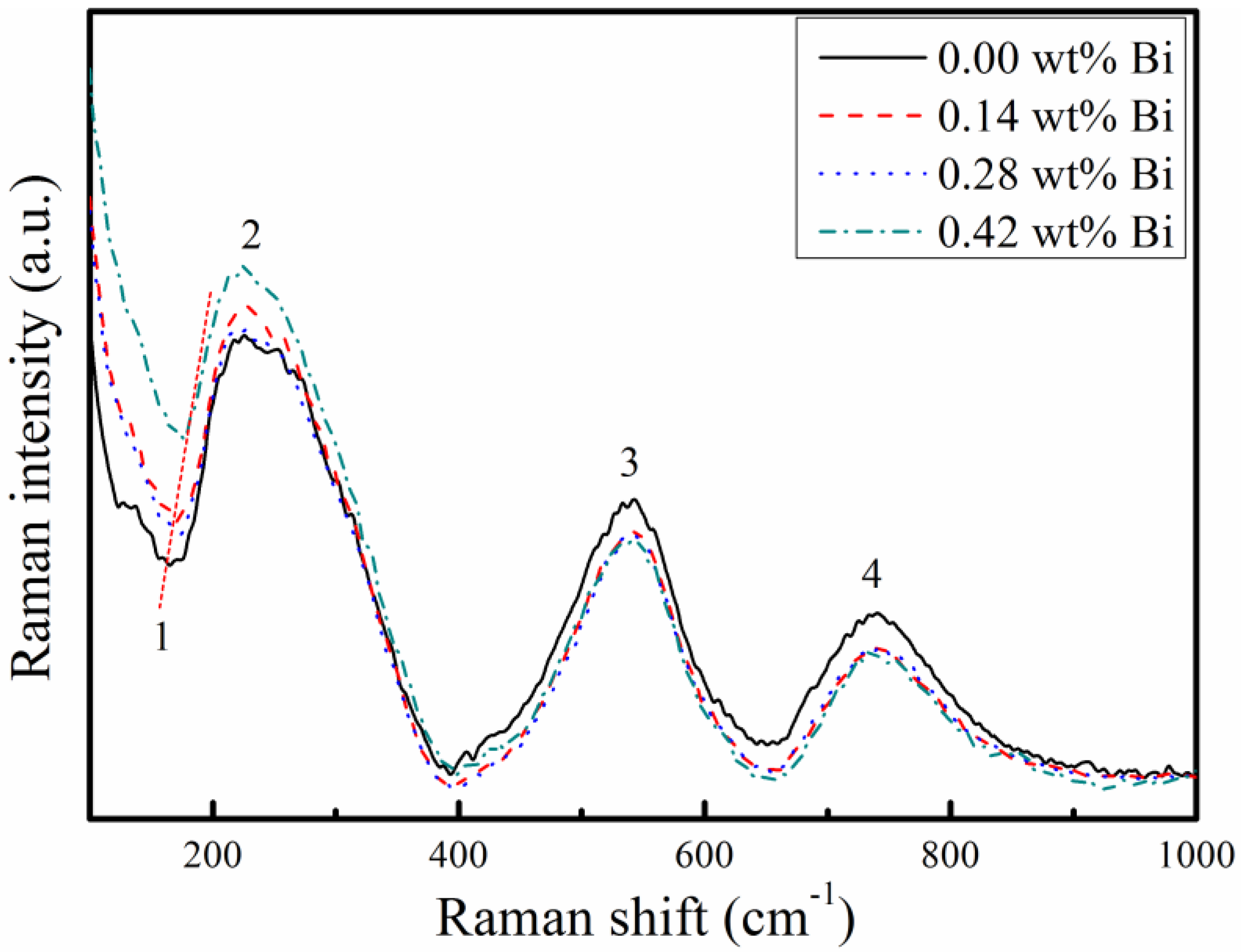
The Raman spectra of PLZT samples were examined and shown in
Figure 2. It has been reported that the modes of perovskite ABO
3 ceramics were assigned to the phase. Some modes were similar to the modes in
Figure 2, including the interference dip at 170 cm
−1, a broad peak at 242 cm
−1, a broad peak at 523 cm
−1, and 724 cm
−1 [
18]. From
Figure 2, it can be found that all samples present a perovskite structure.
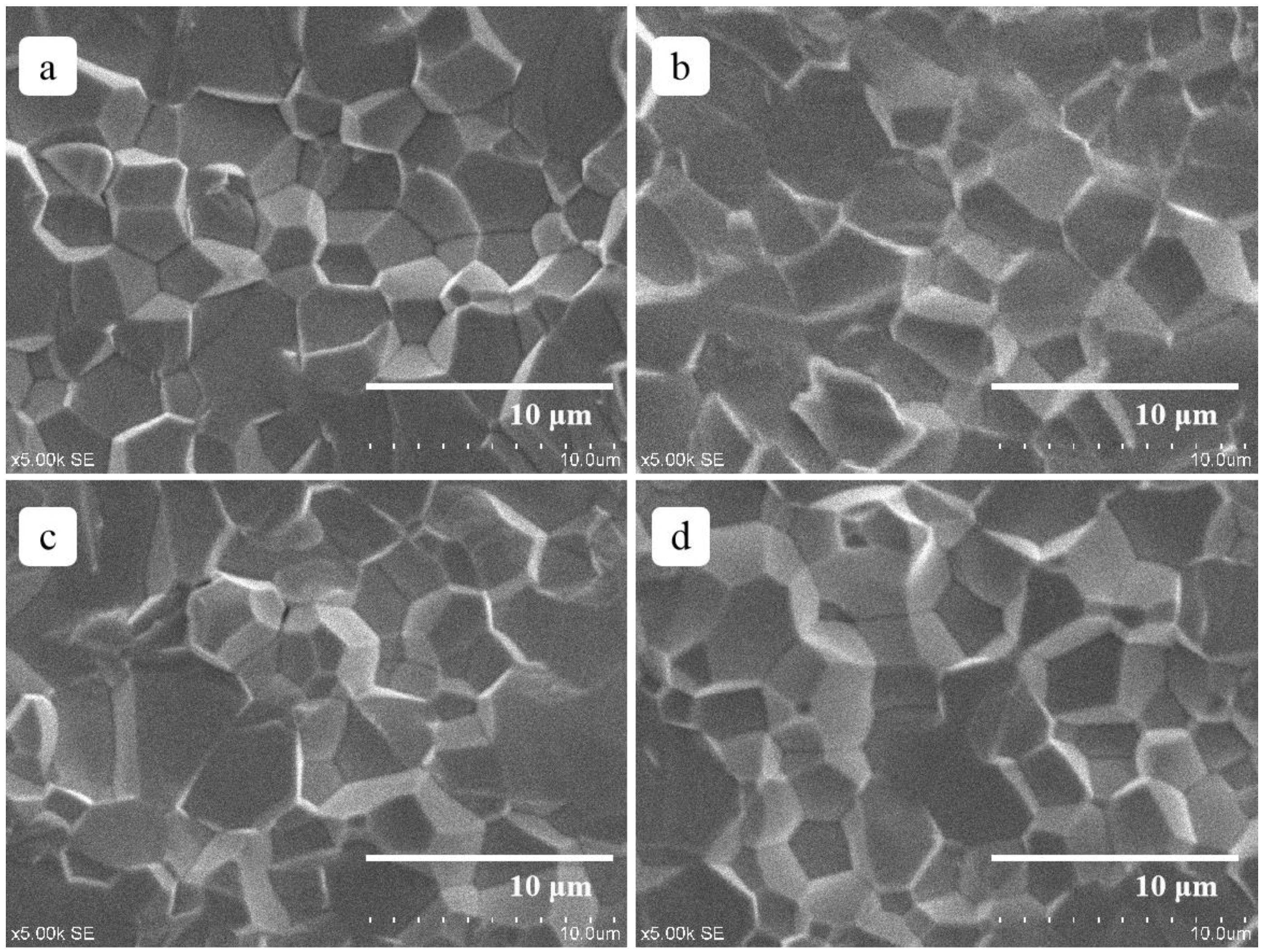
Figure 3 shows the SEM images of Bi-doping PLZT transparent ceramics samples. All samples exhibited a uniform and fully dense microstructure, with a little section of transgranular fractures. The average grain sizes of the ceramic sample, examined by the linear intercept method, were 3.26 μm, 3.52 μm, 3.31 μm, and 3.08 μm respectively as Bi concentration increasing. Compared with undoped PLZT ceramics, PLZT ceramic with 0.14 wt% Bi doping enhanced the grain boundary migration, leading to the growth of grain. But as Bi concentration increased, the grain sizes decreased. The possible explanation for this might be that a higher concentration of Bi
3+ ions near the grain boundaries may restrict the grain growth [
19,
20].
3.2. Dielectric and Ferroelectric Properties
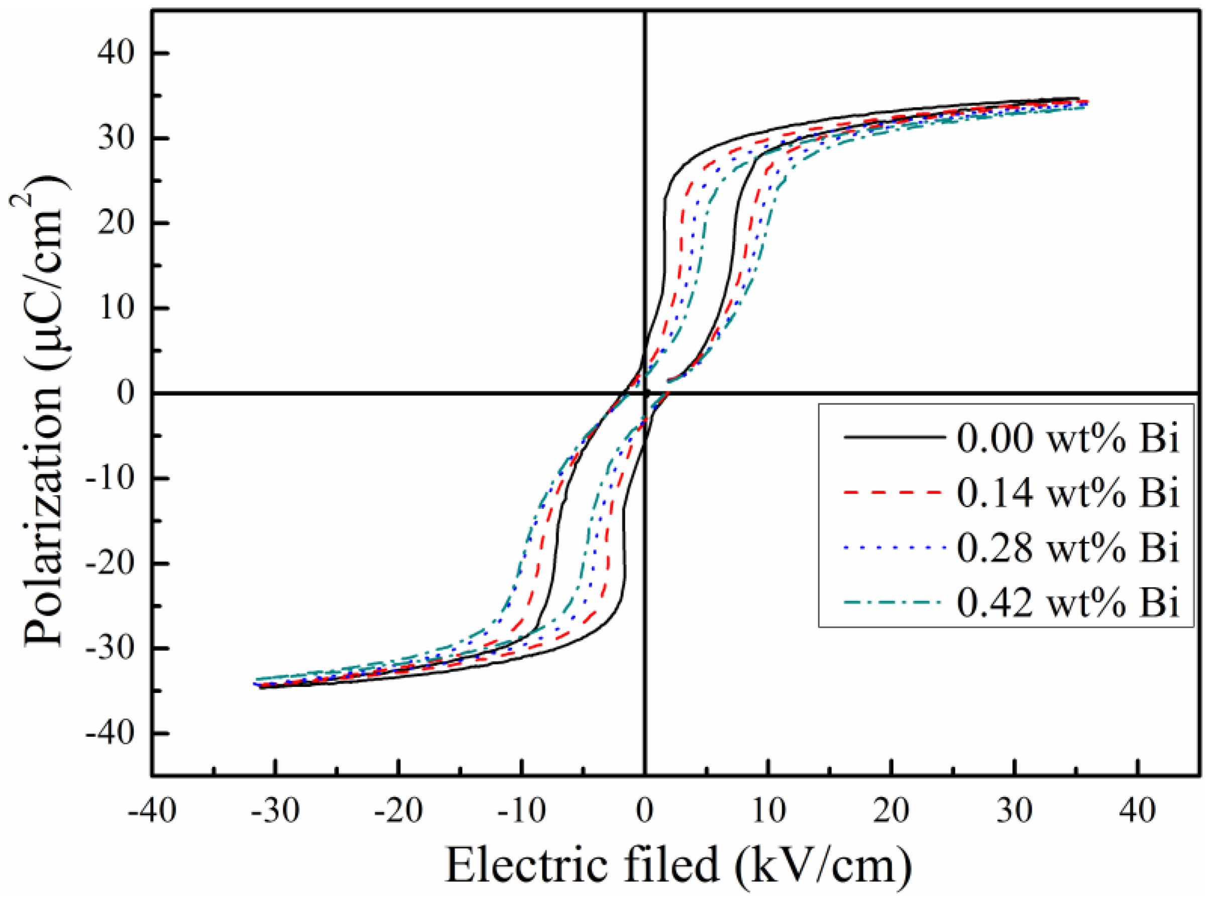
The ferroelectric hysteresis loops of Bi doping PLZT transparent ceramics were shown in
Figure 4. The typical anti-ferroelectric (AFE) phases were observed. The measurement results of remnant polarization (
Pr), saturated polarization (
Ps), and coercive field (
Ec) are all decreased with more Bi
3+ ions doping, see
Table 3. The polarization value and coercive field decreased slightly as the Bi concentration increased. The result was explained by the fact that the modification of Bi-modified for Pb
2+ at A-site could reduce the high polarizability of PLZT ceramics [
21].
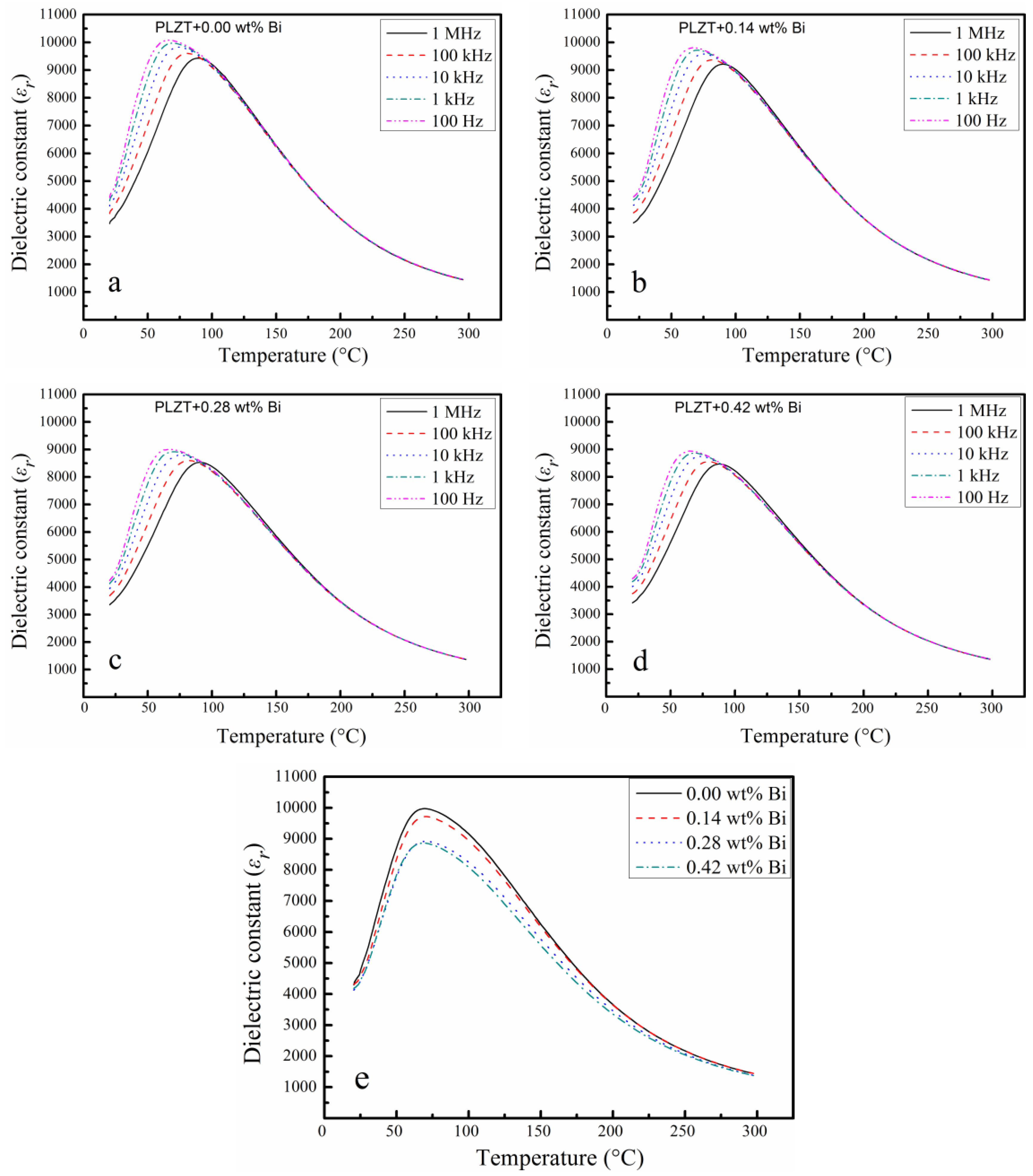
Figure 5 shows the temperature dependence of relative permittivity of Bi doping PLZT ceramics at various frequencies. All the samples in this study exhibited typical relaxor ferroelectric characteristics: broad frequency dispersion nearby as well as the temperature (
Tmax) corresponding to the maximum permittivity. With Bi concentration increasing, the maximum permittivity (
εmax) was decreased, see
Figure 5e. The possible explanation for this might be that the vacancy in the unit cell appeared to maintain the electric neutrality while Bi
3+ ion occupied the A-site. This weakened the coupling of oxygen octahedral established by A-site ions, and further resulted in the dielectric permittivity decreasing.
3.3. Optical Transmittance and Electric-Induced Light Scattering Properties
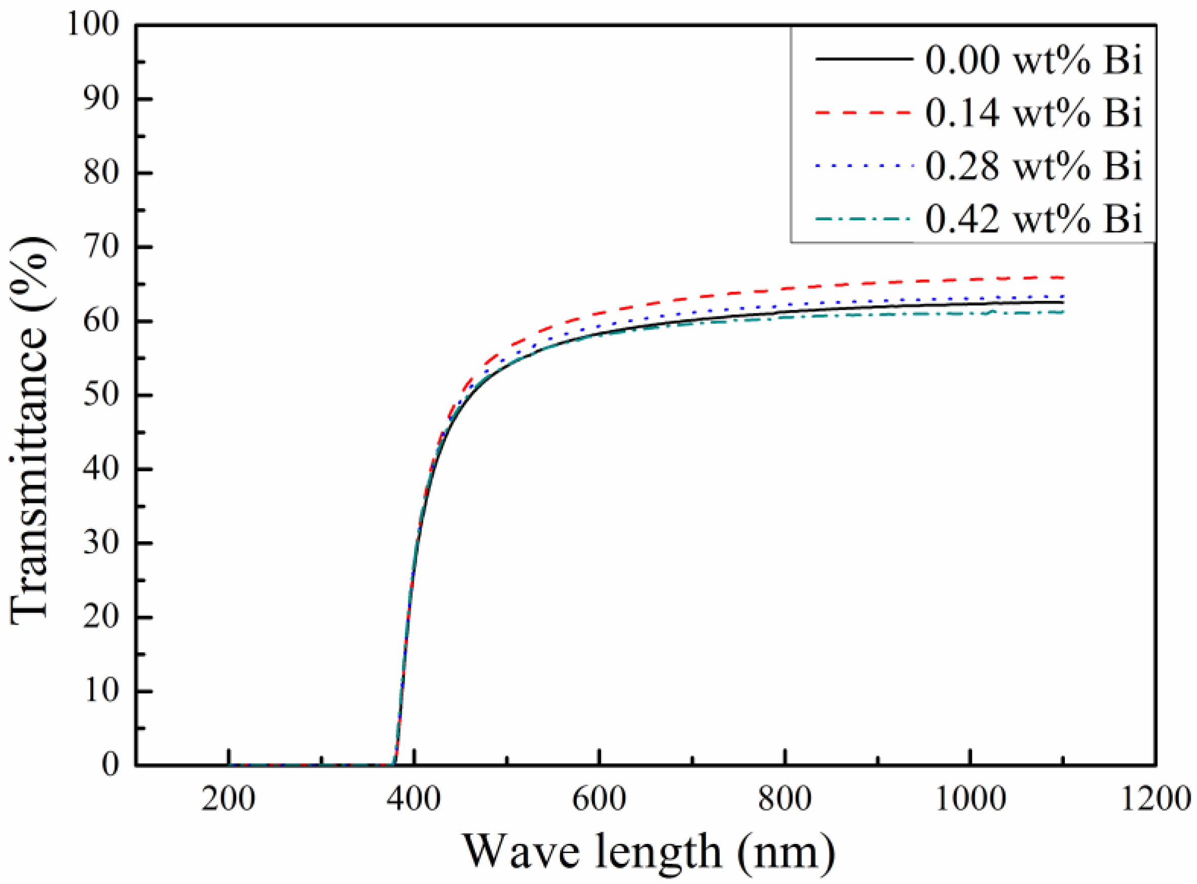
The optical transmittance spectrum of Bi doping PLZT transparent ceramic samples with a thickness of 0.50 mm was shown in
Figure 6. For PLZT transparent ceramics, the refractive index
n is 2.48 at 632.8 nm wavelength, and the optical reflection losses resulting from three-grade air/ceramic interface reflection has been reported to be about 30.22% (
λ = 632.8 nm) [
11]. Therefore, the theoretical transmittance rate of 69% of PLZT ceramics can be derived. It can be observed that all the samples present high transmittance close to the theoretical transmittance level, and the transmittance of the PLZT ceramics with 0.14 wt% Bi doping were improved slightly, see
Figure 6. While the Bi concentration increasing further, the sample transmittance decreased. This phenomenon can be explained by the possibility that small Bi concentration might increase the
c/
a ratio of lattice and enhance the cubic degree, leading to higher transmittance. However, more Bi
3+ ions accumulated at the grain boundaries and restricted the grain growth with Bi concentration increasing further [
20], and the severer light scattering from the more grain boundaries decreased the sample transmittance.
In previous works, it was reported that the PLZT electric-induced light scattering performance could be observed as microdomains grew [
8,
22]. With the suitable size of microdomains, the domain walls would highly influence the light scattering performance. The existence of domain walls would also lower the transmittance of ceramic samples.
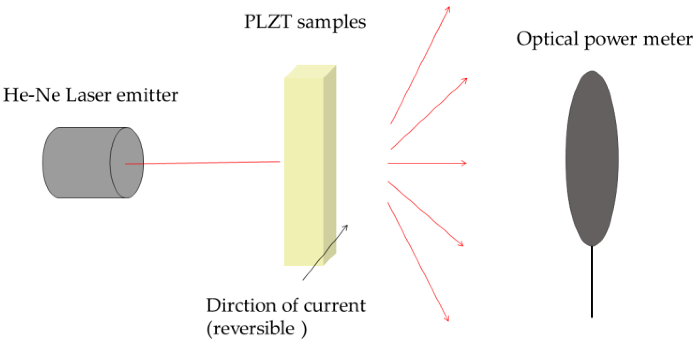
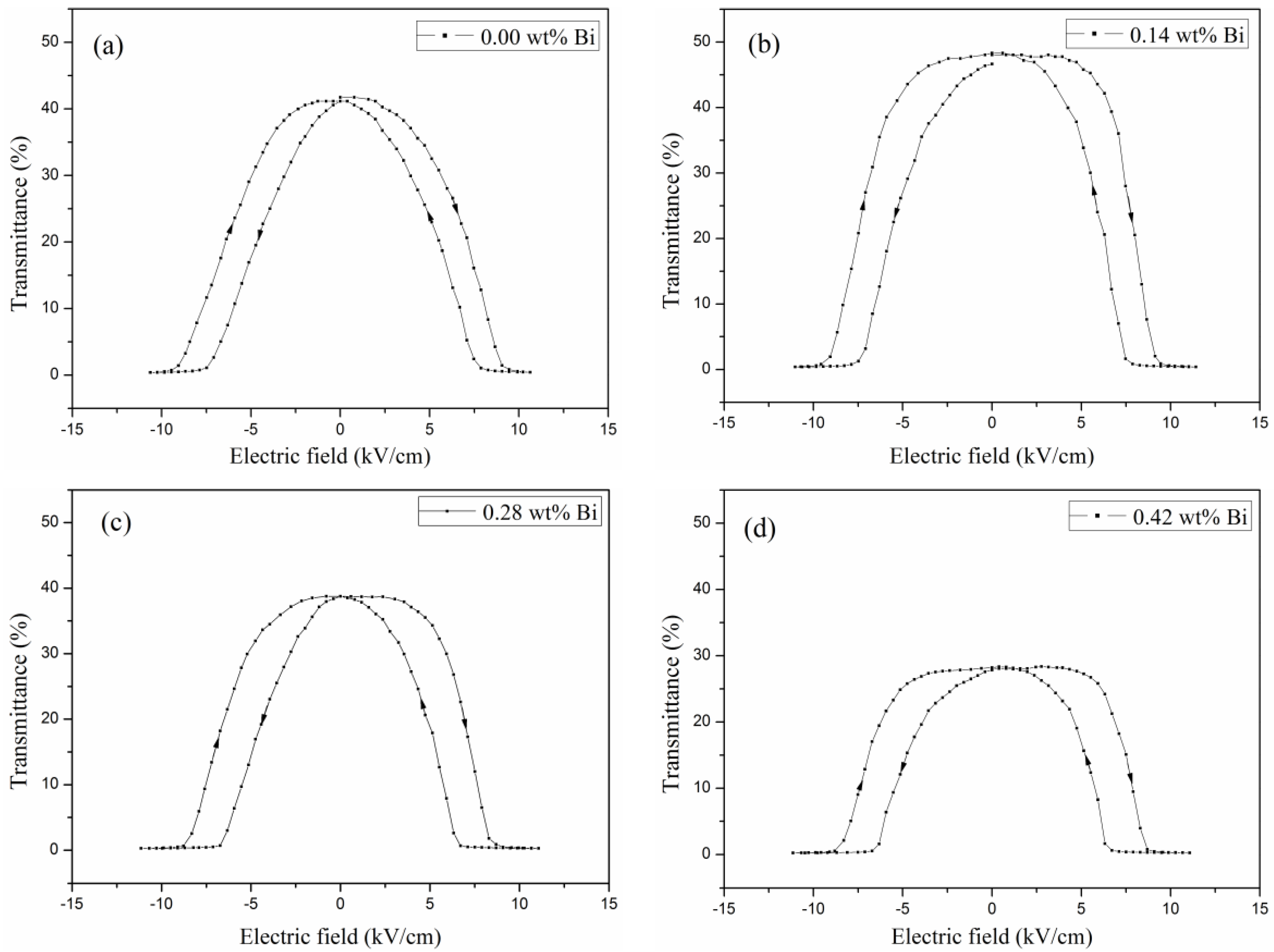
Figure 7 shows the sketch of measurement of PLZT electric-induced light scattering performance.
Figure 8 shows the evolution of transmittance with a changed electric field of PLZT (8.0/69/31) samples with a different Bi concentration at 25 °C. The curves expressed the transmittance variation of PLZT ceramic samples with a variable electric field. All samples were transparent without an electric field and then became opaque for the extensive light scattering effect while a suitable electric field (≥8 kV/cm) was being applied. When the field was removed, the sample transmittance could be recovered. But for the ferroelectric hysteresis property of the PLZT material, a typical hysteresis transmittance curve of the sample was formed. A suitable reversed electric field was found to induce the same light scattering effect. To characterize the light scattering performance concisely, the optical transmittance variation is calculated as the following equation:
where
IE0,
IE, and
I0 are respectively the light intensity without electric field, the light intensity with electric field, and the light intensity without PLZT samples. As the Bi concentration increased, the values of
ΔT of the PLZT transparent ceramic samples were 41.3%, 47.6%, 38.4%, and 27.8% respectively (with a sample thickness of 2.0 mm). It was thought that the amount of domain walls would be increased owing to an enhanced value of remnant polarization (
Pr) [
23]. In this study, while the electric field removed, the
Pr value of the PLZT ceramic sample decreased as the Bi concentration increasing. This variation may cause the sample transmittance to be improved while the electric field is being removed. Combined with the optical transmittance properties in
Figure 6, an optimized
ΔT value of 47.6% has been obtained in the PLZT ceramic sample with 0.14 wt% Bi doping. This promotion of electric-induced light scattering performance would provide the Bi-doped PLZT (8.0/69/31) ceramics with major potential in specific light modulators.
4. Conclusions
PLZT (8.0/69/31) EO ceramics with Bi doping were fabricated by a hot-press process for the first time. The XRD analysis confirmed that the Bi3+ ions entered the A-site of perovskite ABO3 structure of PLZT ceramics. With Bi concentration increasing, the remnant polarization value (Pr), saturated polarization (Ps), coercive field (Ec), and the maximum permittivity (εmax) became smaller. 0.14 wt% Bi concentration could improve the electric-induced light scattering performance and optical transmittance of PLZT transparent ceramics. The PLZT (8.0/69/31) EO ceramic sample with 0.14 wt% Bi doping presented a higher optical transmittance of 61.8% (λ = 633 nm) and the maximum light deduction value of ~47.6%.
Author Contributions
X.H. participated in the conceptualization. X.H., S.Z., B.Z., X.Z. and P.Q. participated in the methodology and carried out the experiments. X.H., B.Z., X.Z., L.L. and D.S. participated in the data measurement and analysis. X.H., S.Z., B.Z. and X.Z. participated in the writing—review and editing. All authors helped in the original draft preparation, then read and approved the final manuscript.
Funding
This research was funded by the National Natural Science Foundation of China (Grant No. 51602327), Institute Innovation Leading Special Project of Taicang City (Grant No. TC2018DYDS09), the National Key Research and Development Program of China (2016YFB0701004), the Key Laboratory of Transparent Optical Inorganic Materials of Chinese Academy of Sciences (KLTOIM-2016-07), and the Science and Technology Commission of Shanghai Municipality (16070502700) for supporting the research.
Conflicts of Interest
The authors declare no conflicts of interest.
References
- Haertling, G.H.; Land, C.E. Hot-pressed (Pb,La)(Zr,Ti)O3 ferroelectric ceramics for electro-optic applications. J. Am. Ceram. Soc. 1971, 54, 1–11. [Google Scholar] [CrossRef]
- Smith, W.D.; Land, C.E. Scattering-Mode Ferroelectric-Photoconductor Image Storage and Display Devices. Appl. Phys. Lett. 1972, 20, 169–171. [Google Scholar] [CrossRef]
- Uchino, K. Electro-optic ceramics and their display applications. Ceram. Int. 1995, 21, 309–315. [Google Scholar] [CrossRef]
- Rai, R.; Sharma, S. Structural and dielectric properties of Sb-doped PLZT ceramics. Ceram. Int. 2004, 30, 1295–1299. [Google Scholar] [CrossRef]
- Kumada, A.; Toda, G.; Otomo, Y. An electrooptic image storage device using field induced reversible transitions between AFE and FE phases of PLZT ceramics. Ferroelectrics 1974, 7, 367–369. [Google Scholar] [CrossRef]
- Xia, B.; He, X.; Sun, D.; Cheng, W.; Qiu, P.; Zeng, X. The electrically controlled light scattering performances of PLZT transparent ceramics. Ceram. Int. 2015, 41, S246–S249. [Google Scholar] [CrossRef]
- Zeng, X.; He, X.; Cheng, W.; Qiu, P.; Xia, B. Effect of Dy substitution on ferroelectric, optical and electro-optic properties of transparent Pb0.90La0.10 (Zr0.65Ti0.35)O3 ceramics. Ceram. Int. 2014, 40, 6197–6202. [Google Scholar]
- Zhang, X.; Xia, B.; Zeng, X.; Qiu, P.; Cheng, W.; He, X. Temperature Dependence of Electric-induced Light Scattering Performance for PLZT Ceramics. J. Am. Ceram. Soc. 2014, 97, 1389–1392. [Google Scholar] [CrossRef]
- Stojanovic, B.D.; Zaghete, M.A.; Paiva-Santos, C.O.; Cilense, M.; Magnani, R.; Longo, E.; Varela, J.A. Hot-pressed 9.5/65/35 PLZT prepared by the polymeric precursor method. Ceram. Int. 2000, 26, 625–630. [Google Scholar] [CrossRef]
- Cerqueira, M.; Nasar, R.S.; Leite, E.R.; Longo, E.; Varela, J.A. Sintering and characterization of PLZT (9/65/35). Ceram. Int. 2000, 26, 231–236. [Google Scholar]
- Xia, B.; He, X.; Zheng, X.; Qiu, P.; Cheng, W.; Zeng, X. Electrically induced light scattering performances of lanthanum-modified lead zirconate titanate transparent ceramics. J. Electroceram. 2012, 29, 192–197. [Google Scholar] [CrossRef]
- Qiao, P.; Zhang, Y.; Chen, X.; Zhou, M.; Wang, G.; Dong, X. Enhancing pyroelectric properties in (Pb1−1.5xLax)(Zr0.86Ti0.14)O3 ceramics through composition modulated phase transition. Ceram. Int. 2019, 45, 7114–7119. [Google Scholar] [CrossRef]
- Dutta, S.; Choudhary, R.N.P.; Sinha, P.K. Structural, dielectric and electrical properties of Al+ 3-modified PLZT ceramics. Mater. Lett. 2004, 58, 2735–2740. [Google Scholar] [CrossRef]
- Dutta, S.; Choudhary, R.N.P.; Sinha, P.K. Impedance spectroscopy studies on Fe3+ ion modified PLZT ceramics. Ceram. Int. 2007, 33, 13–20. [Google Scholar] [CrossRef]
- Limpichaipanit, A.; Ngamjarurojana, A. Effect of Li and Bi co-doping and sintering temperature on dielectric properties of PLZT 9/65/35 ceramics. Ceram. Int. 2017, 43, 4450–4455. [Google Scholar] [CrossRef]
- Rai, R.; Sharma, S.; Choudhary, R.N.P. Structural and dielectric properties of Bi modified PLZT ceramics. Solid State Commun. 2005, 133, 635–639. [Google Scholar] [CrossRef]
- Shannon, R.D. Revised effective ionic radii and systematic studies of interatomic distances in halides and chalcogenides. Acta Cryst. 1976, 32, 751–767. [Google Scholar] [CrossRef]
- Zhou, M.; Liang, R.; Zhou, Z.; Xu, C.; Nie, X.; Dong, X. Enhanced Curie temperature and piezoelectric properties of (Ba0.85Ca0.15)(Zr0.10Ti0.90)O3 lead-free ceramics after the addition of LiTaO3. Mater. Res. Bull. 2018, 106, 213–219. [Google Scholar] [CrossRef]
- Fraygola, B.M.; Chandrasekaran, A.; Bahati, D.; Salazar, U.; Biancoli, A.; Marzari, N.; Damjanovic, D.; Setter, N. Piezoelectric softening by Nb substitution in (Ba, Pb) ZrO3 ceramics. J. Am. Ceram. 2017, 100, 1885–1895. [Google Scholar] [CrossRef]
- Kumar, B.P.; Sangawar, S.R.; Kumar, H.H. Structural and electrical properties of double doped (Fe3+ and Ba2+) PZT electroceramics. Ceram. Int. 2014, 40, 3809–3812. [Google Scholar] [CrossRef]
- Kainz, T.; Bitschnau, B.; Mautner, F.A.; Reichmann, K. Comparison of Lanthanum and Bismuth modification of lead Zirconate-Lead Titanate PZT-A structural and dielectric study. J. Eur. Ceram. Soc. 2016, 36, 507–514. [Google Scholar] [CrossRef]
- Yao, X.; Chen, Z.; Cross, L.E. Polarization and depolarization behavior of hot pressed lead lanthanum zirconate titanate ceramics. J. Appl. Phys. 1983, 54, 3399–3403. [Google Scholar]
- Yin, Q.R. Microstructure, Property and Processing of Functional Ceramics; Metallurgical Industry Press: Beijing, China, 2005; pp. 46–58. [Google Scholar]
© 2019 by the authors. Licensee MDPI, Basel, Switzerland. This article is an open access article distributed under the terms and conditions of the Creative Commons Attribution (CC BY) license (http://creativecommons.org/licenses/by/4.0/).


