Effect of Selective Laser Melting Process Parameters on the Quality of Al Alloy Parts: Powder Characterization, Density, Surface Roughness, and Dimensional Accuracy


Abstract
1. Introduction
2. Experimental Procedure
2.1. Material
2.2. Design of Experiment
2.3. SLM Process Parameters
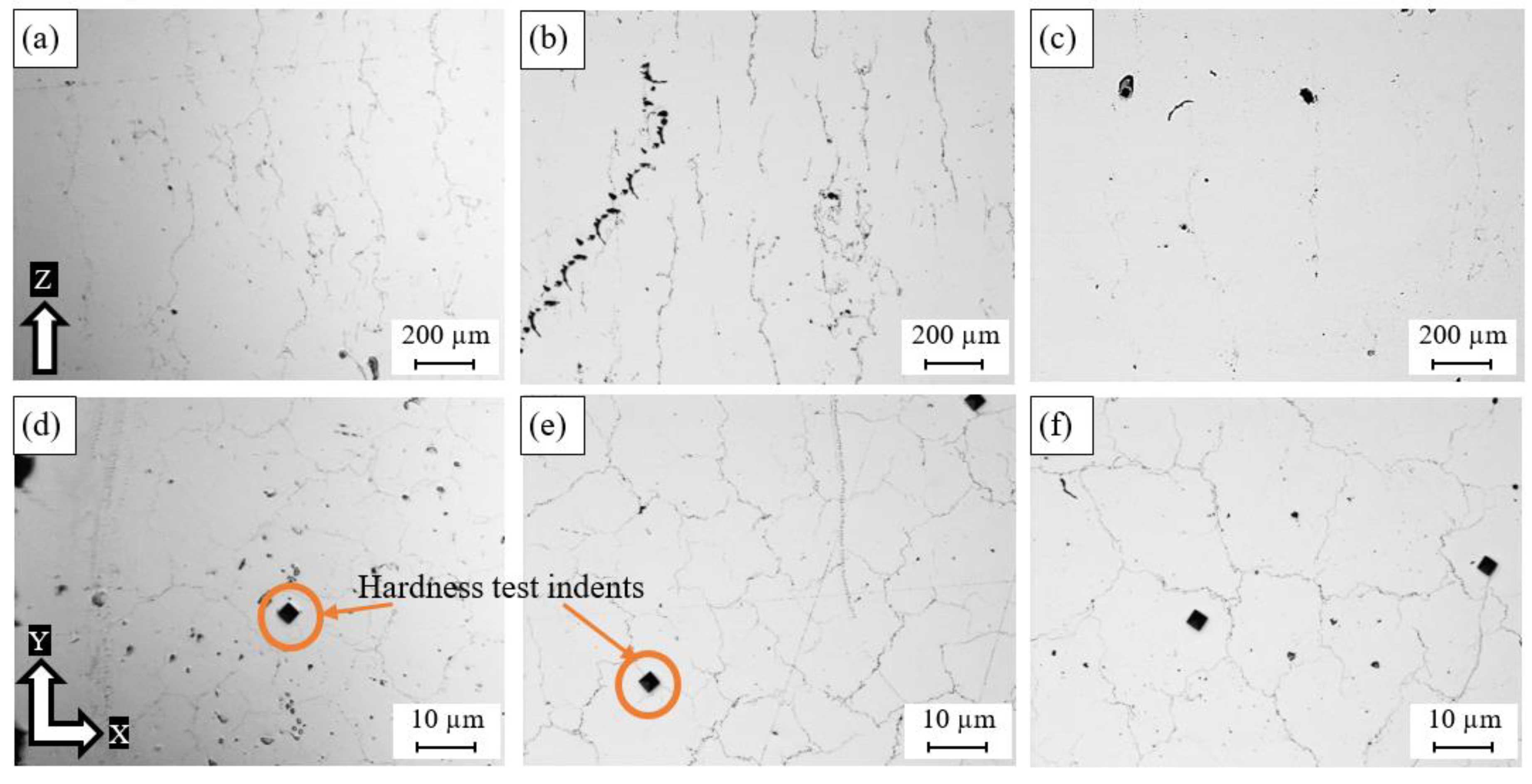
2.4. Sample Characterization Method
3. Results and Discussion
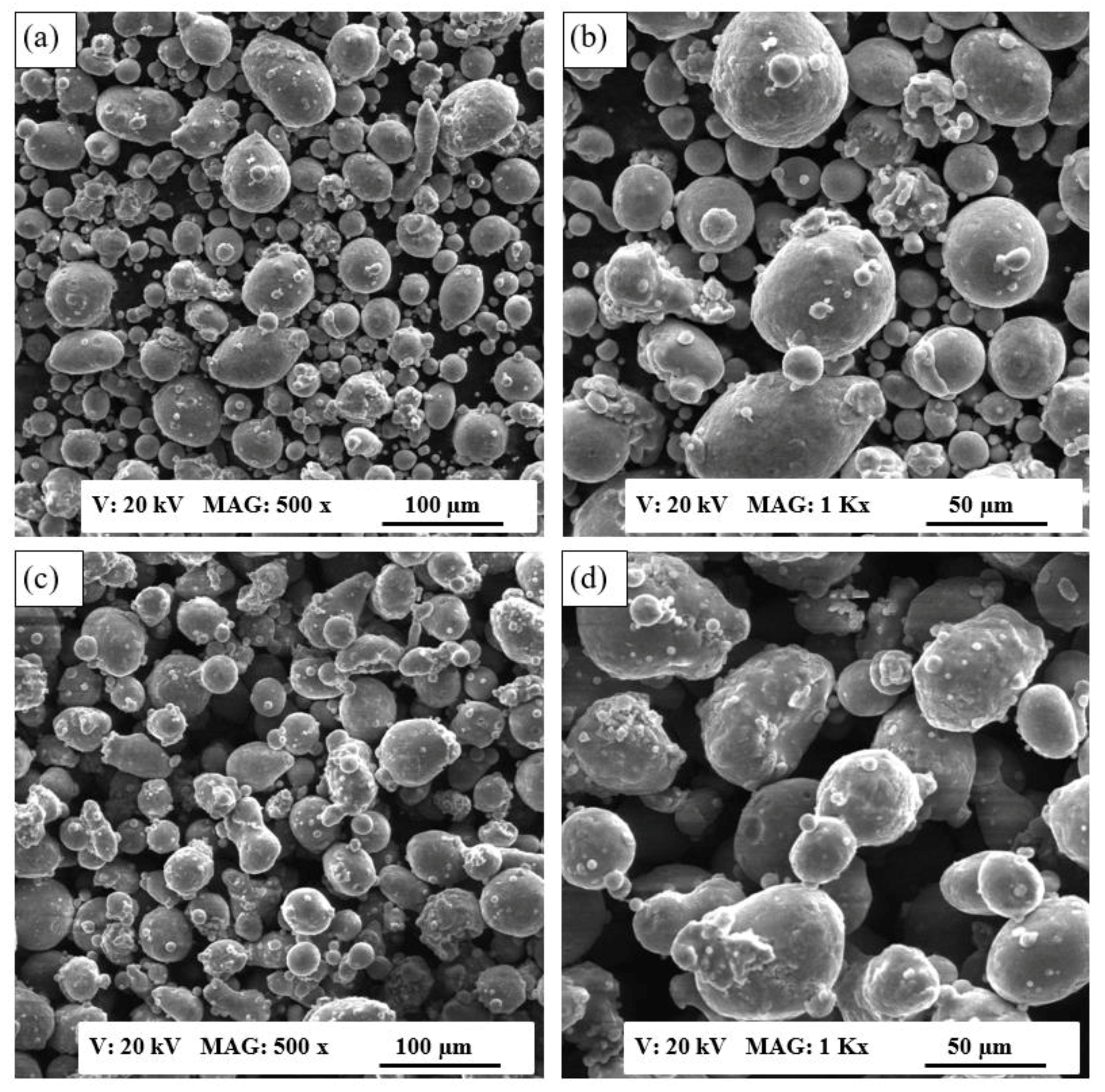
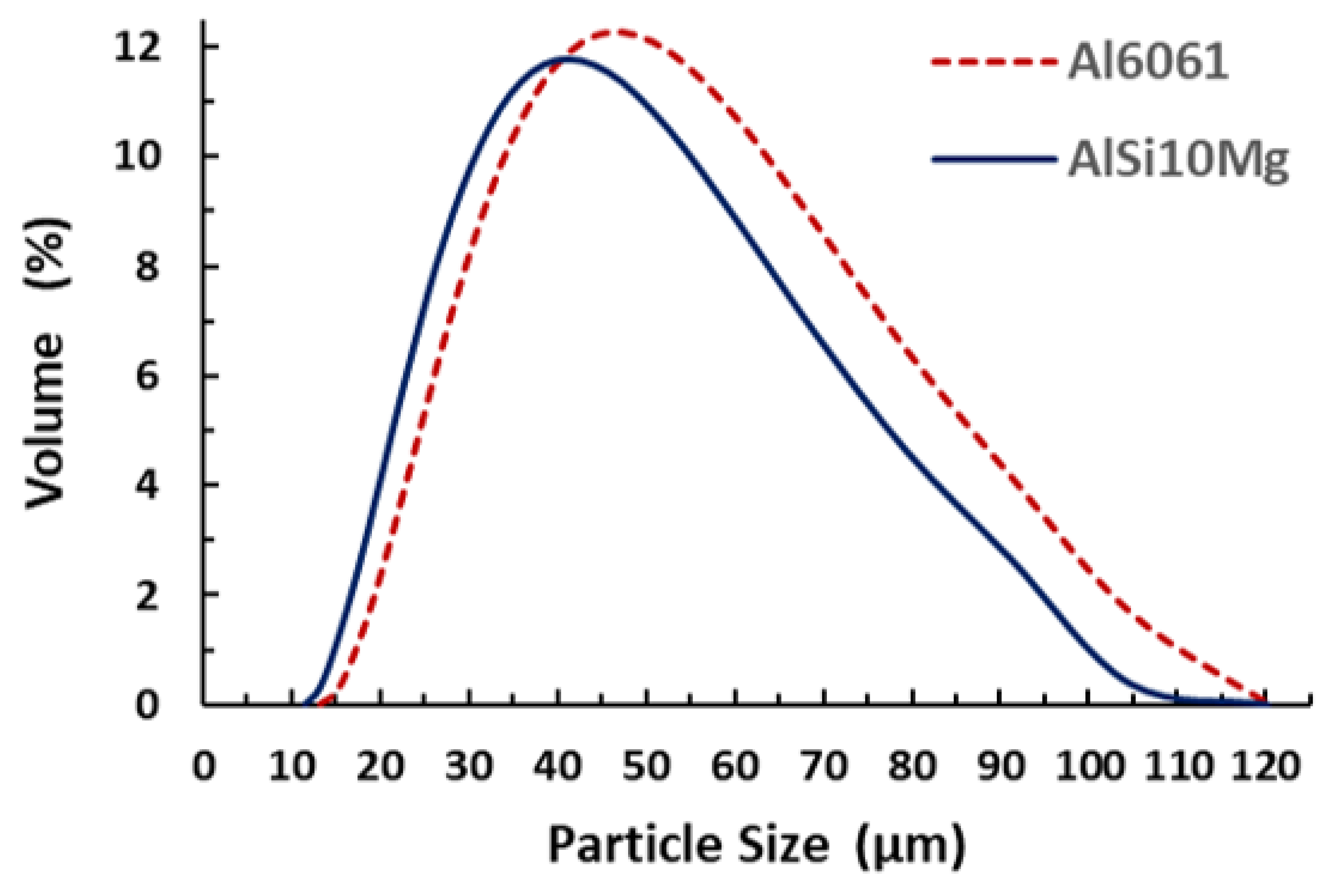
3.1. Powder Characterization
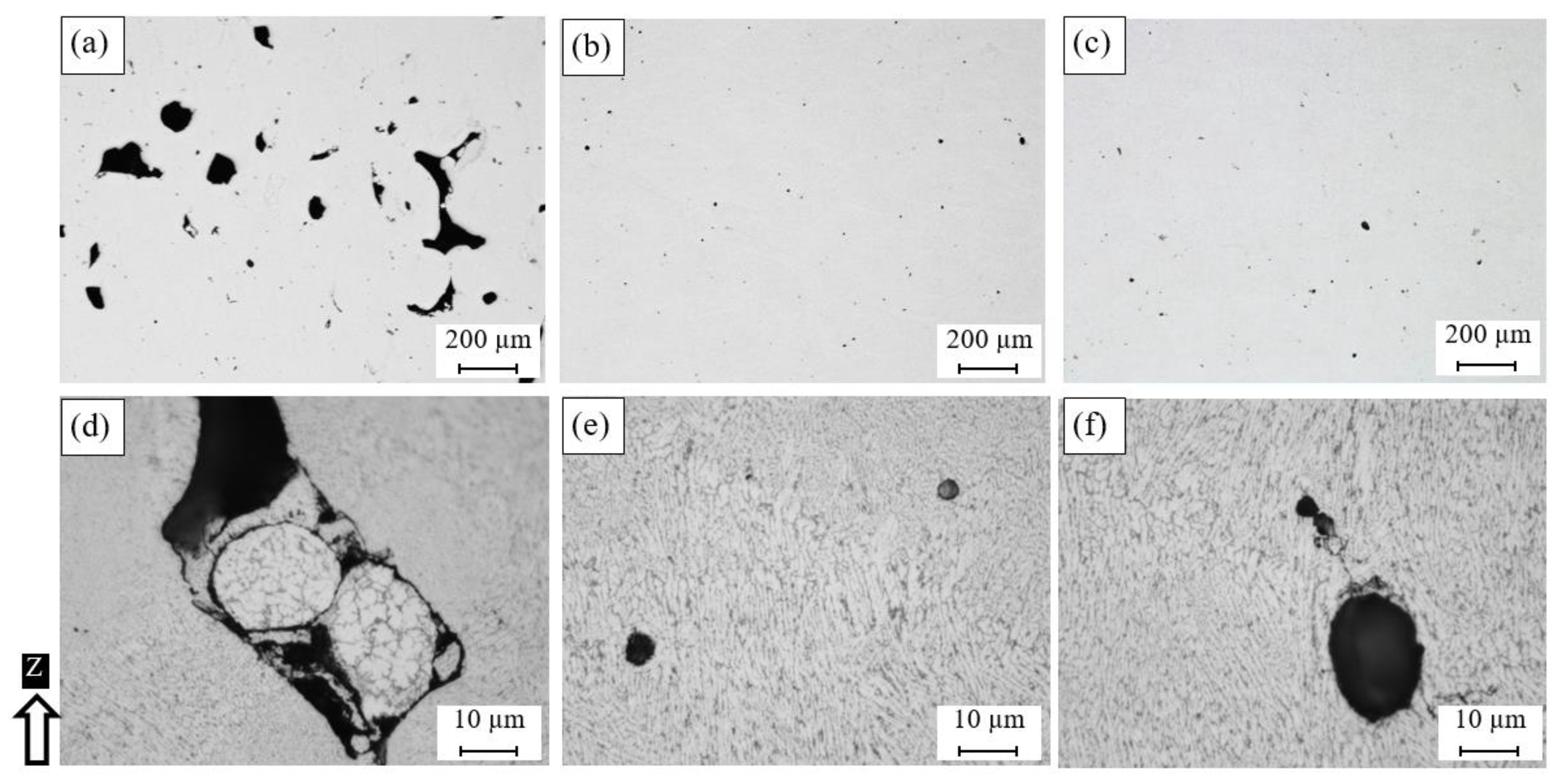
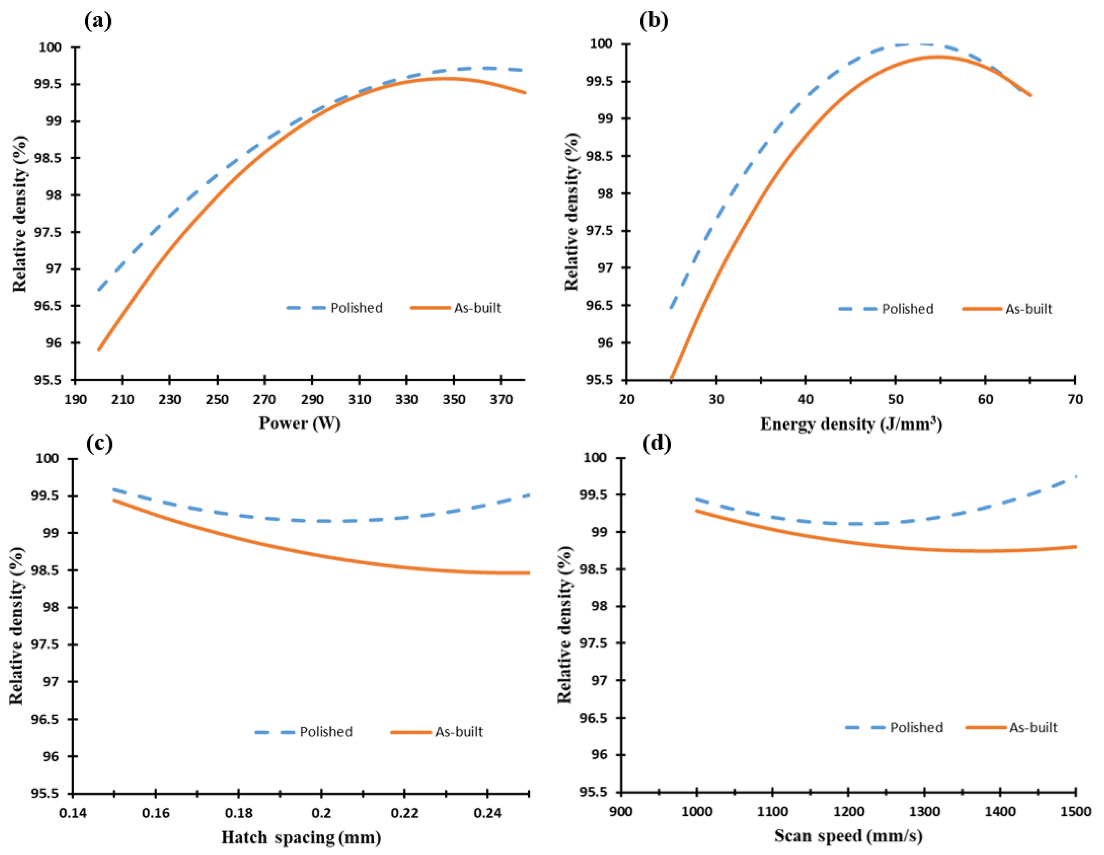
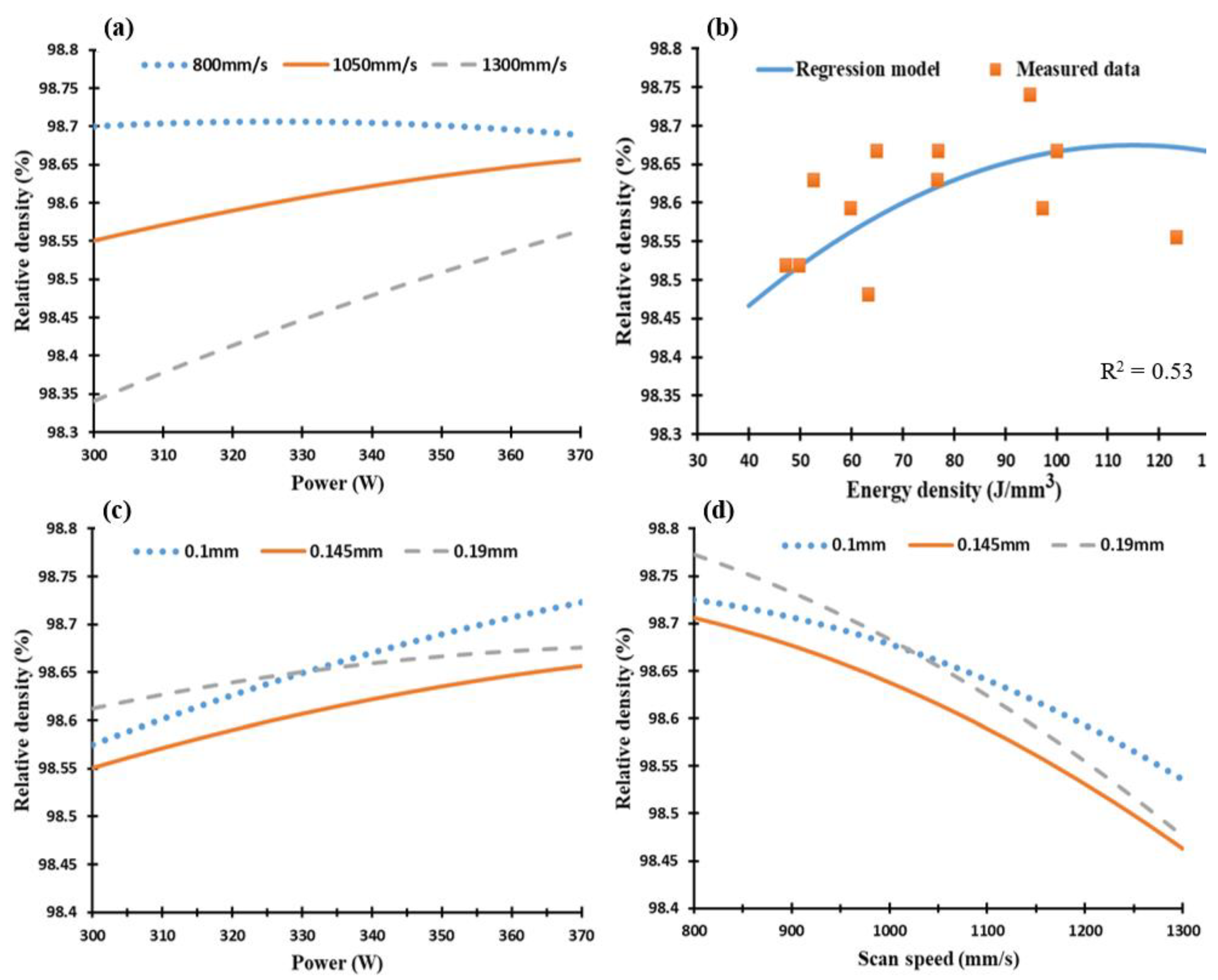
3.2. Relative Density
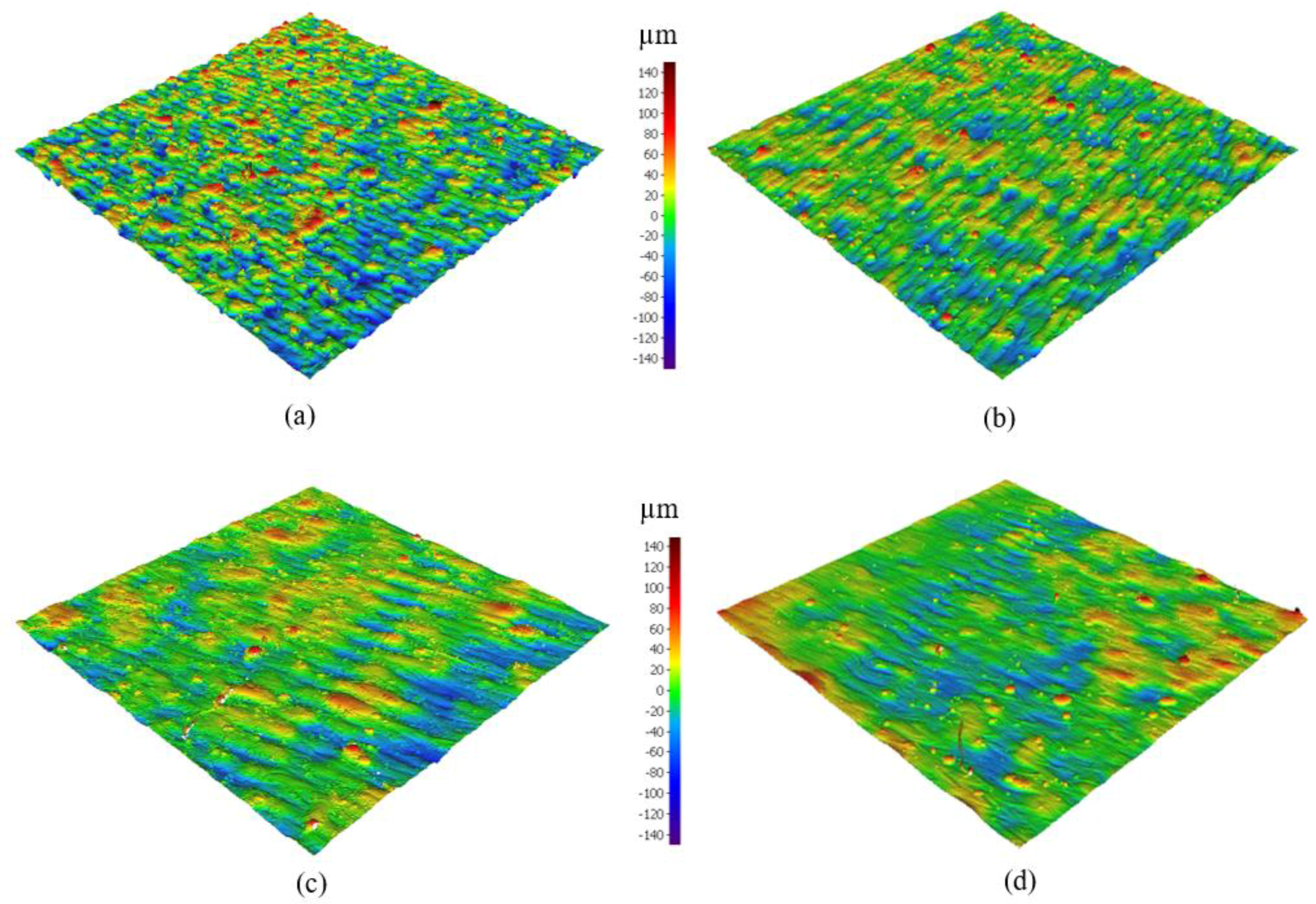
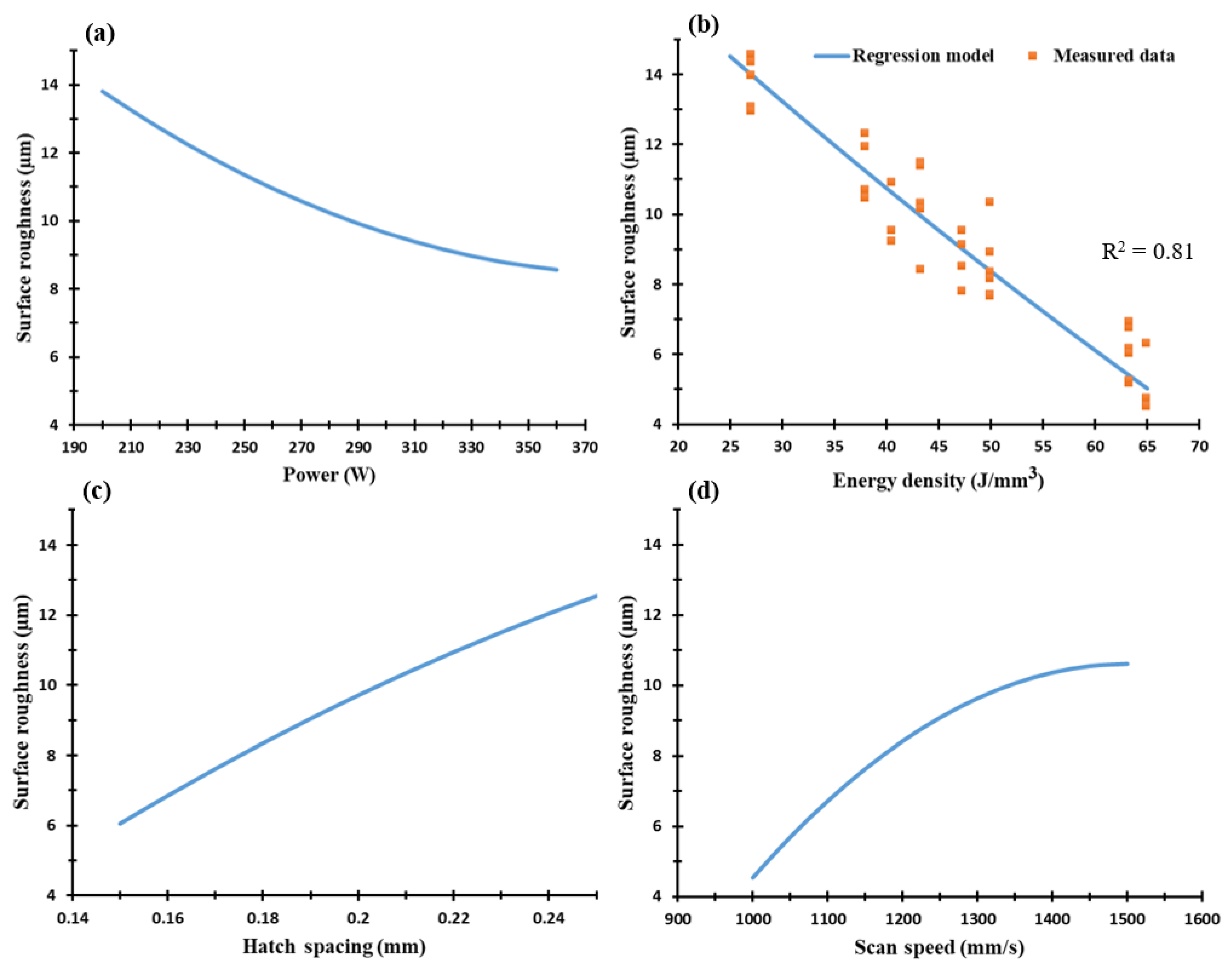
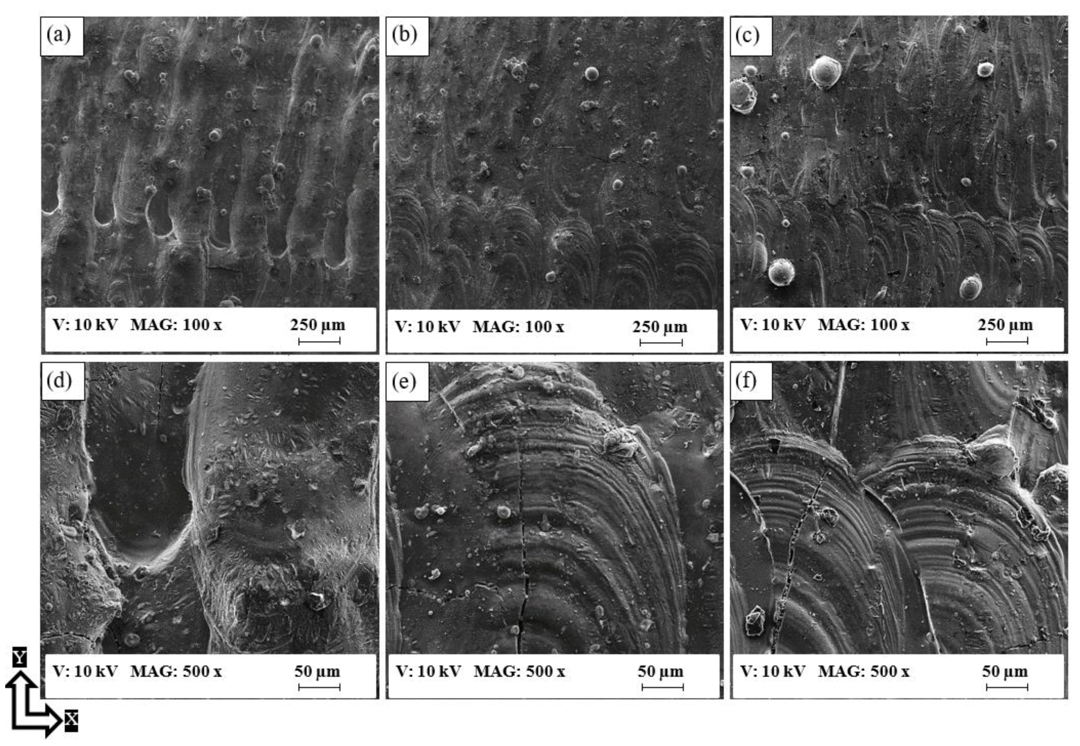
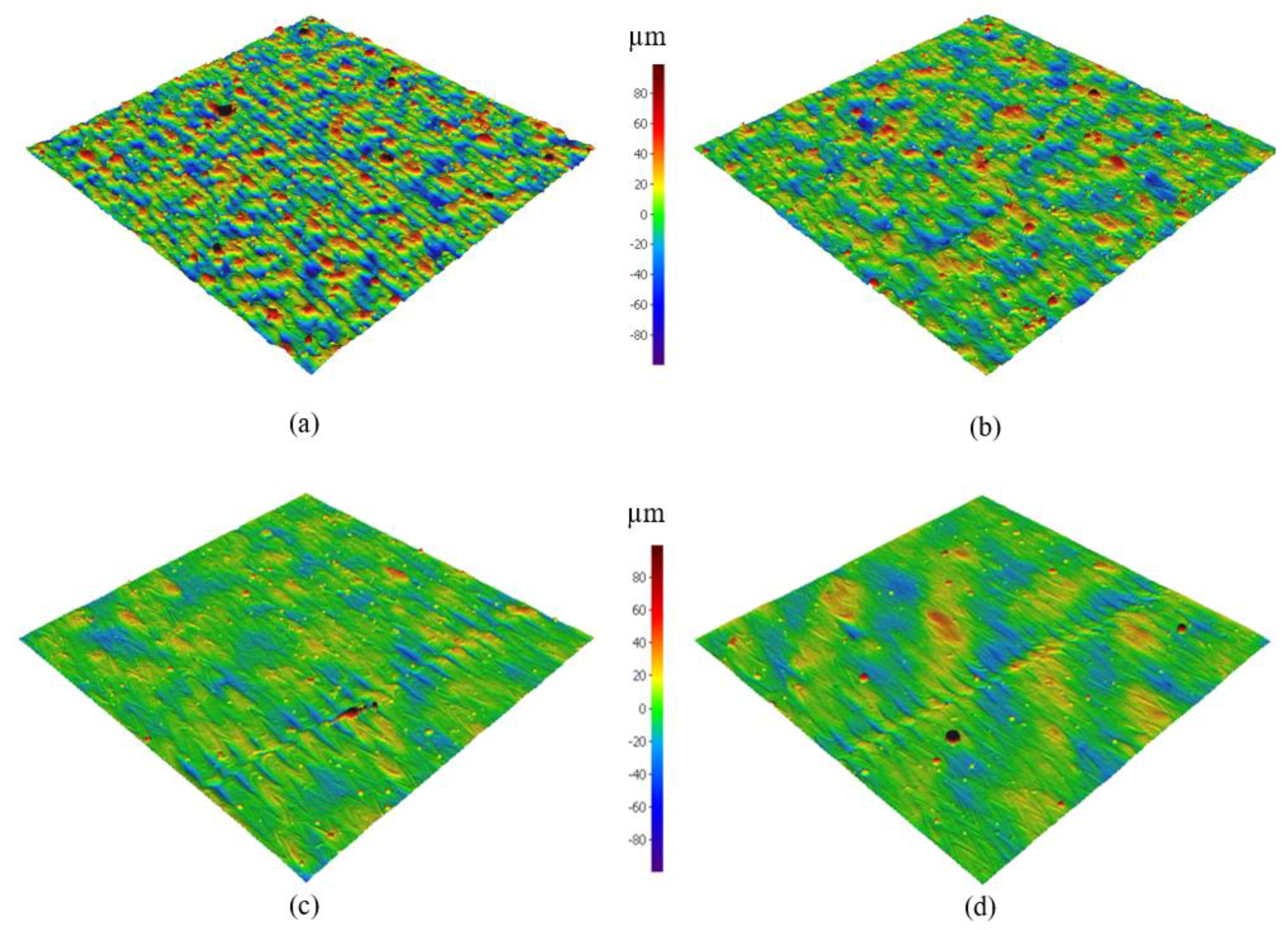
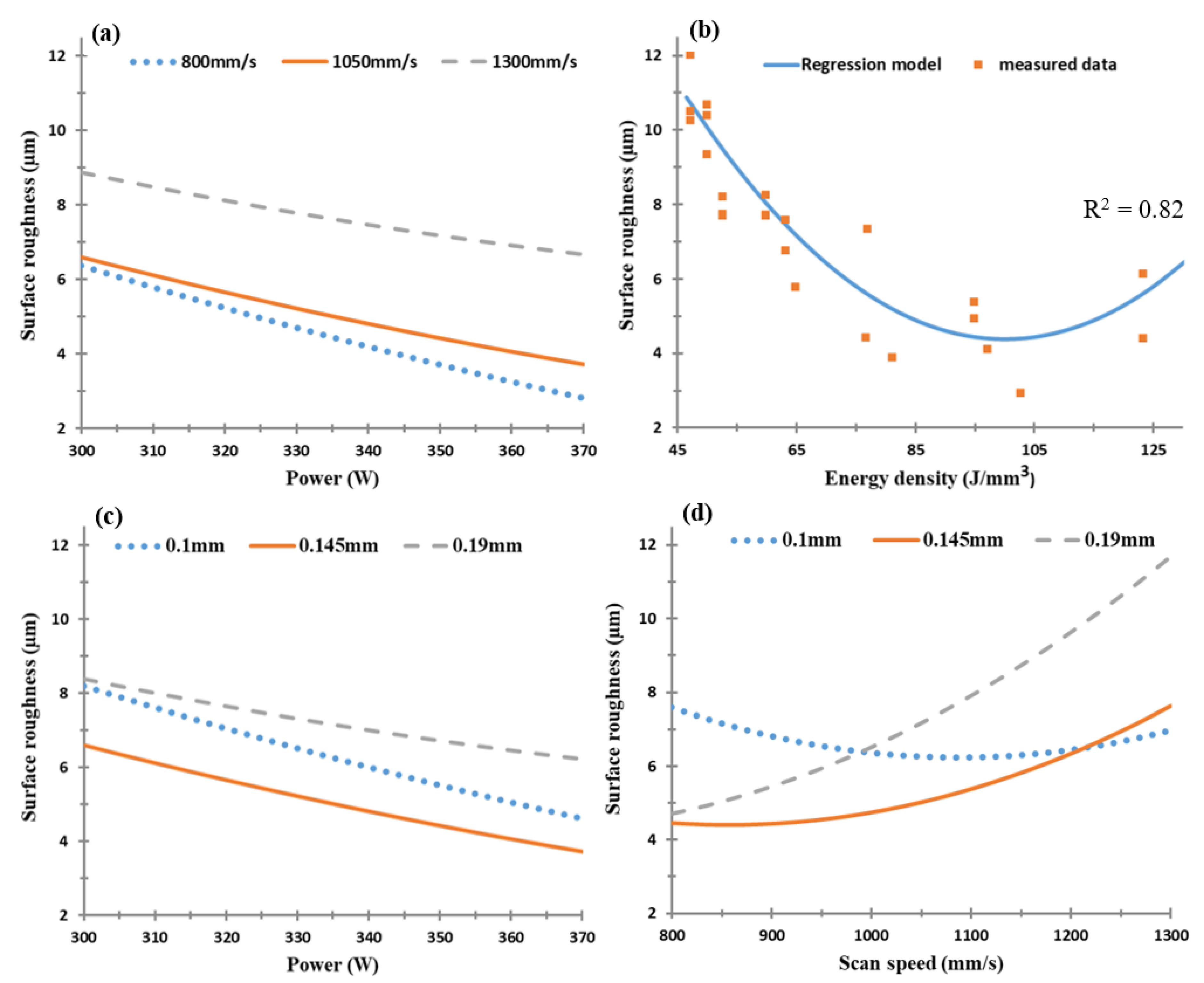
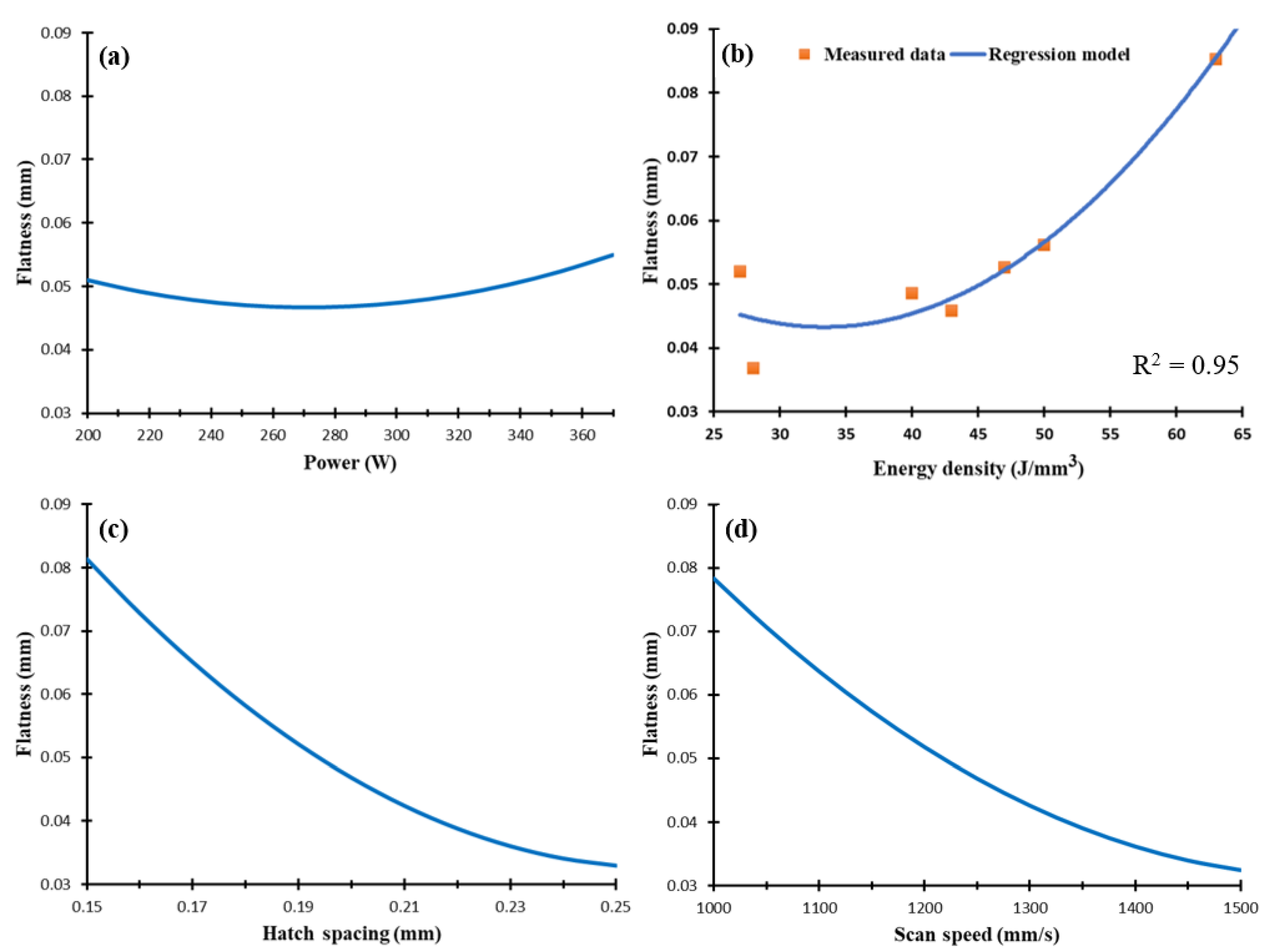
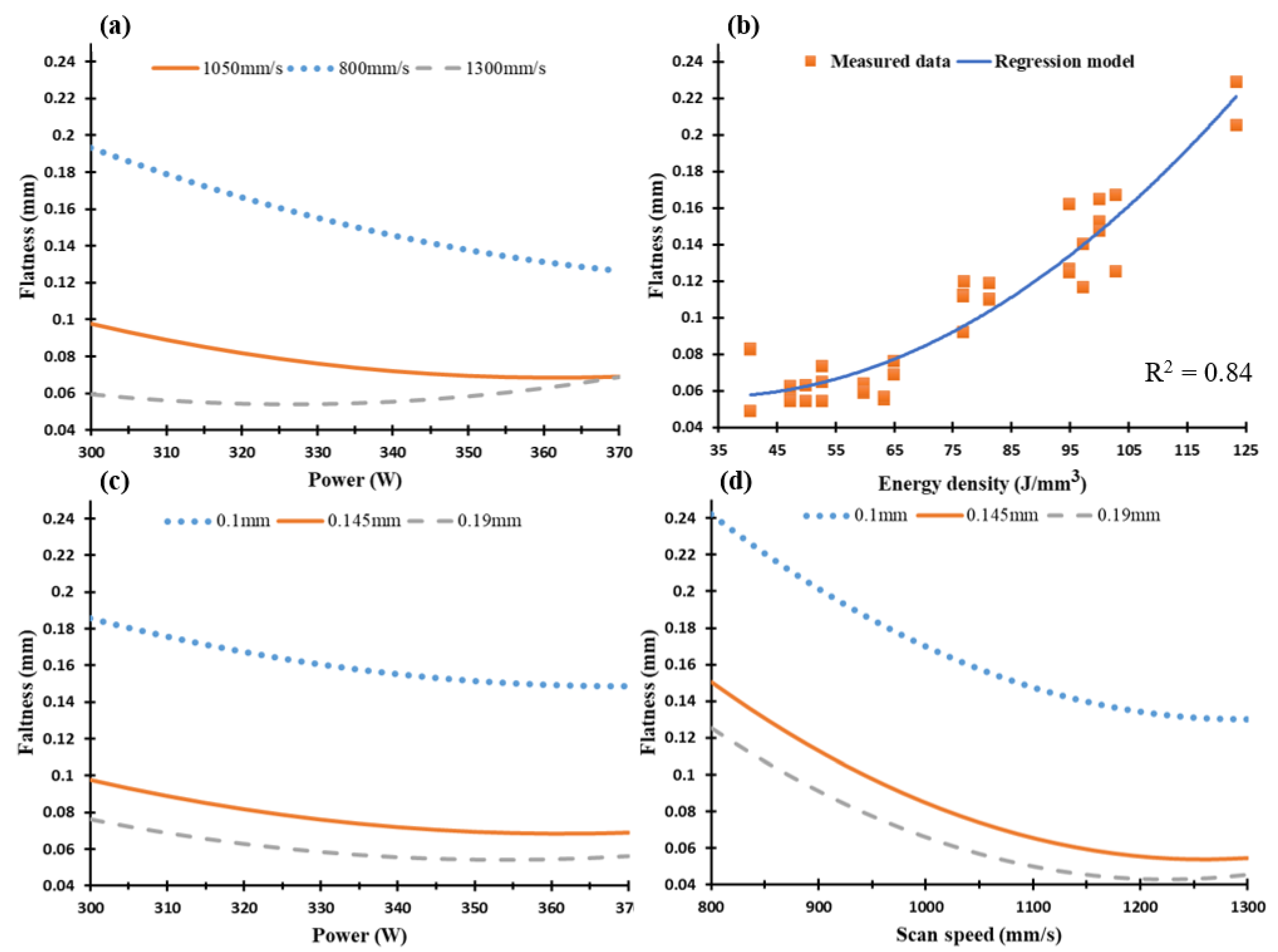
3.3. Surface Topology
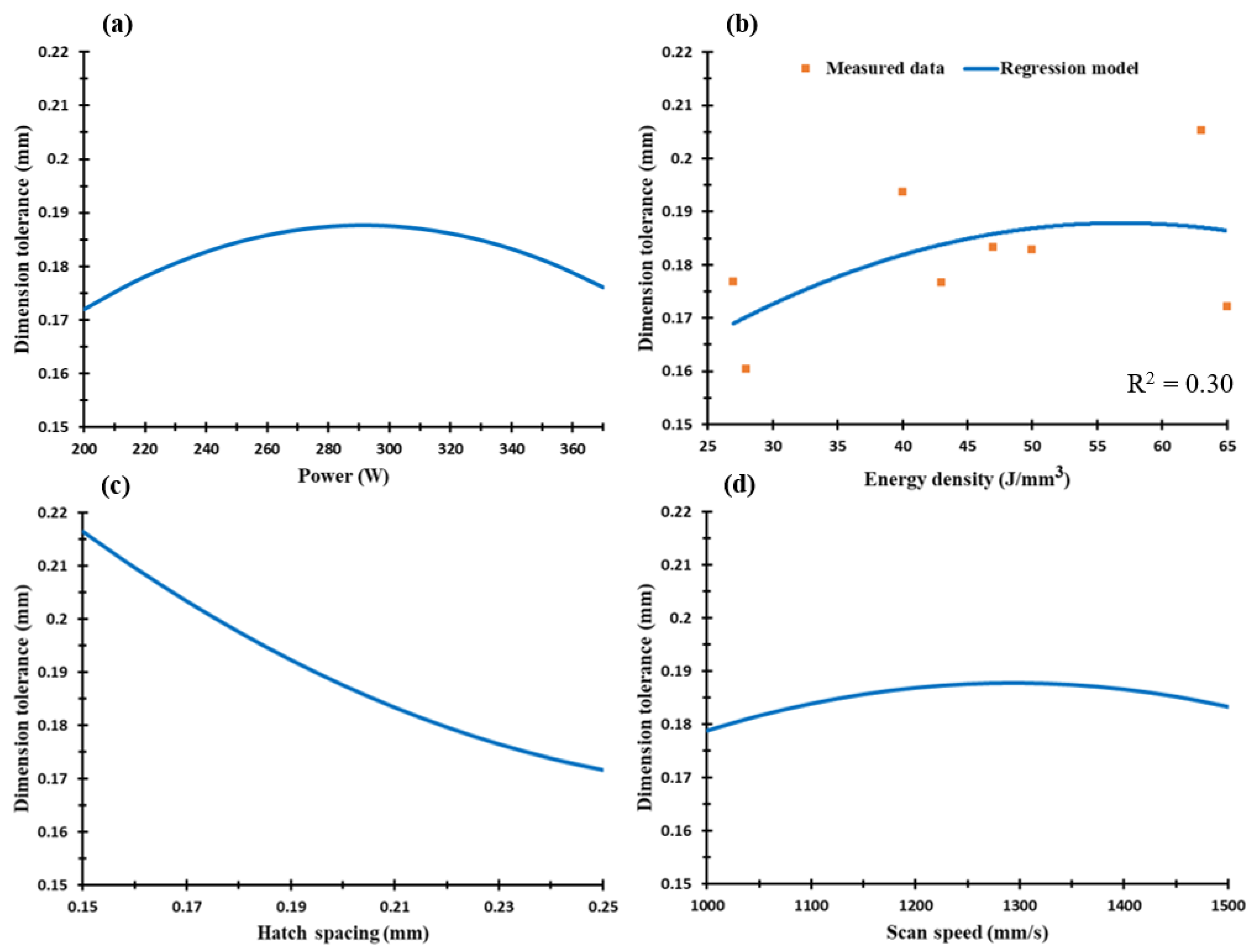
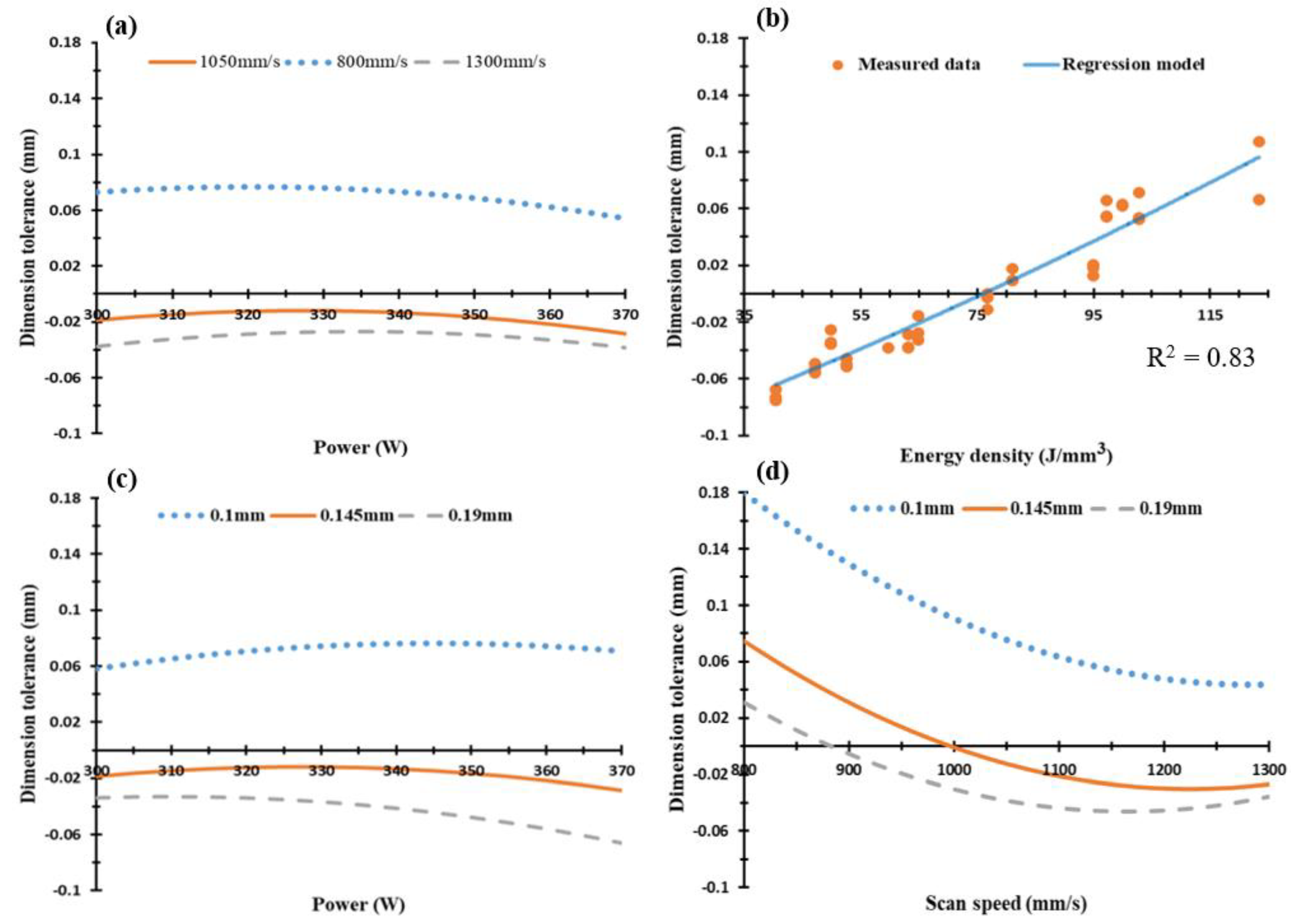
3.4. Dimensional Accuracy
4. Summary and Conclusions
- Powder morphology revealed that AlSi10Mg and Al6061 possess a spherical particle shape interspersed with of elongated particles in a considerable percentage. PSD showed a positively skewed distribution within a range of 12–120 µm.
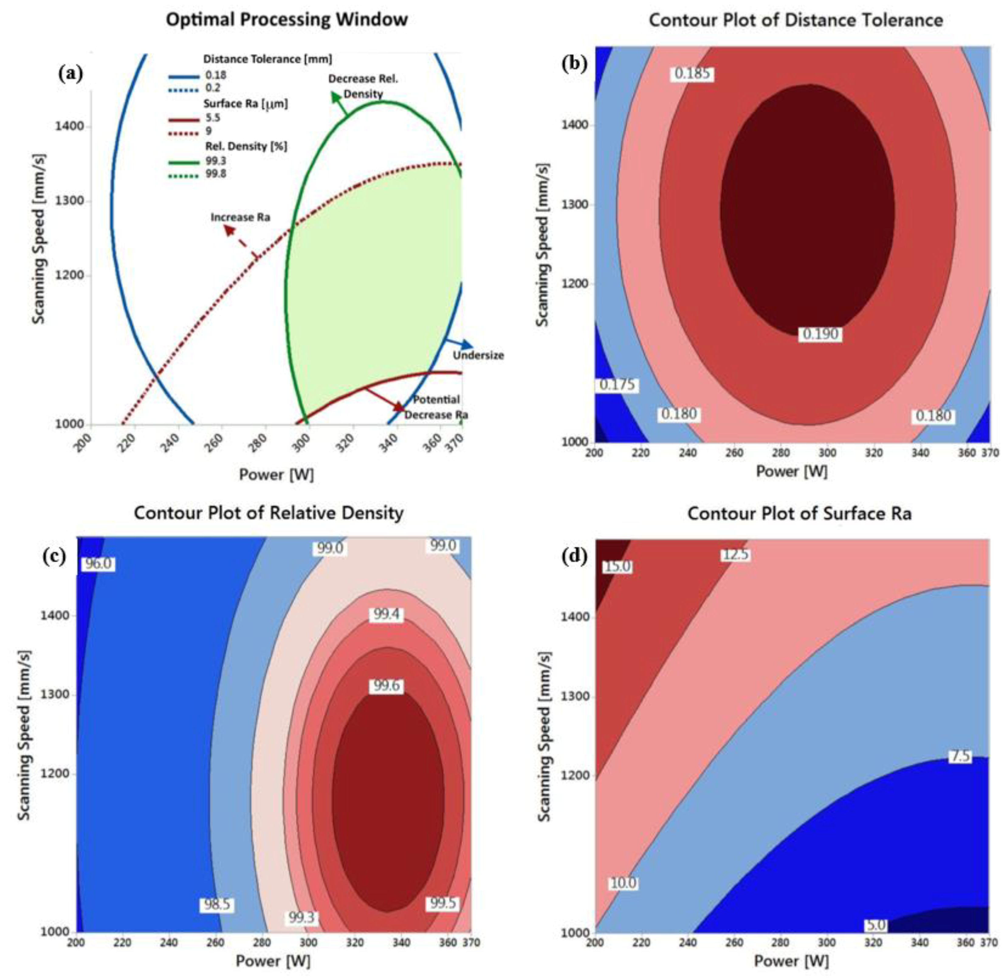
- The rate of energy density affected the relative density and porosity formation inside the as-built parts. The optimum range of energy density was 50–60 J/mm3, which resulted in relative density reaching 99.7%. The relative density of the polished samples reached 99.9%, with a 0.1% internal porosity. The higher rates of energy densities contributed to the formation of large hydrogen spherical pores, while the lower rates resulted in keyhole pores because of the lack of powder fusion.
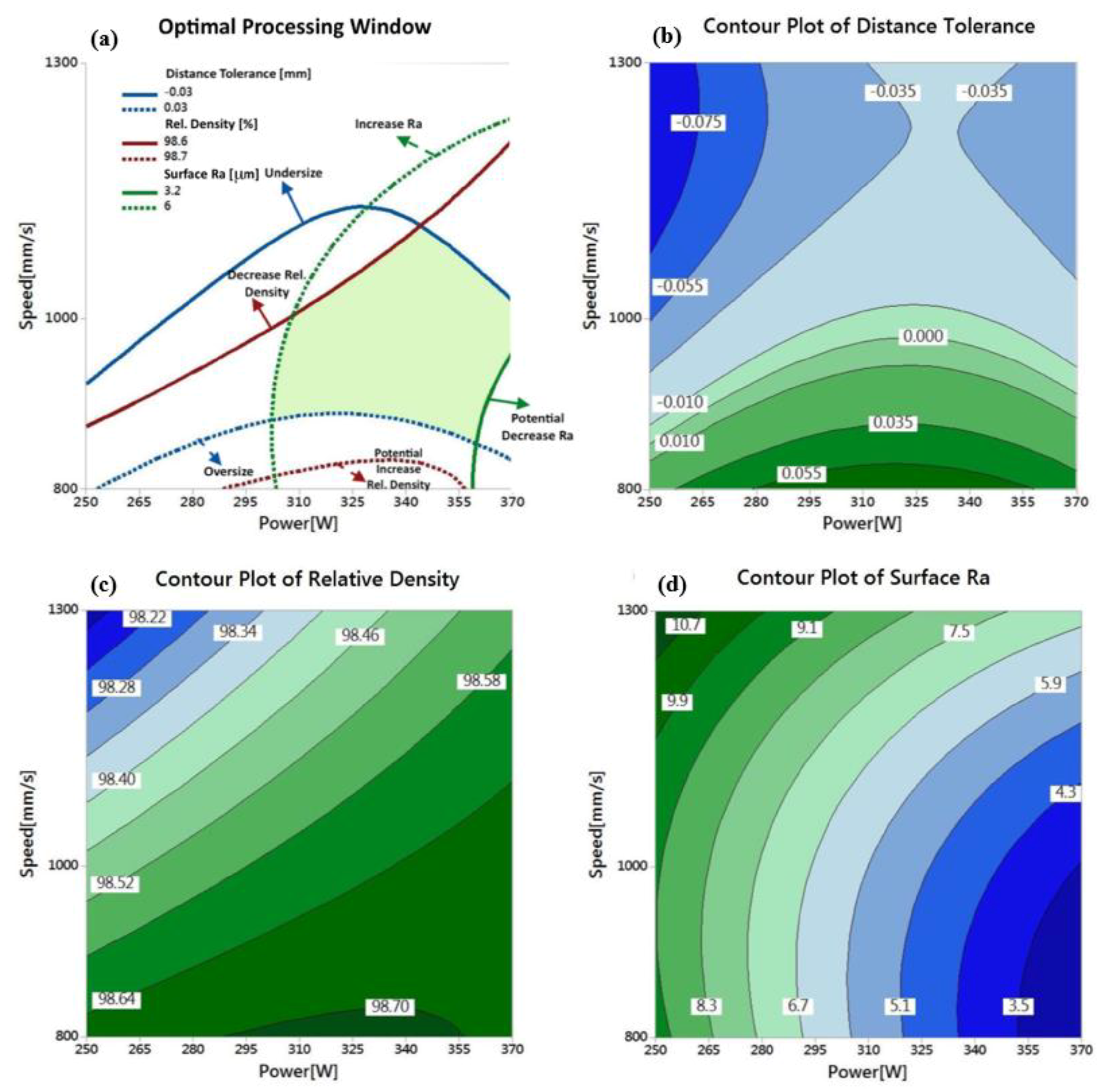
- For the Al6061, the maximum relative density measured was 98.72% using an energy density of 102.8 J/mm3 and an 800 mm/s scan speed. A relationship between the scan speed and the laser power was noted, whereby the highest relative density was achieved at a low scan speed and high laser power. The relative density of the Al6061 parts showed lower values compared to the relative density of AlSi10Mg, due to lower Si content, which increased the CTE and caused the formation of hot cracks inside the as-built Al6061 parts.
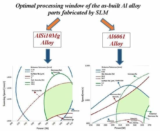
- The surface topology was significantly affected by the energy density applied to both materials. The surface roughness reduced alongside the increase of energy density. For the AlSi10Mg samples, the minimum surface roughness was 4.5 µm at 65 J/mm3. For the Al6061 parts, an energy density of 102.8 J/mm3 resulted in the best surface roughness of 3 µm. The energy density was limited to a maximum of 65 J/mm3 for AlSi10Mg and to 123.3 J/mm3 for Al6061, to avoid delamination and failure of part building.
- For AlSi10Mg, the dimensional tolerance varied between an oversize of 0.15 and 0.195 mm. The best surface flatness could be obtained with higher hatch spacing and scan speeds.
- For the Al6061 parts, the lowest dimensional tolerance was achieved using an energy density of 76.8 J/mm3. Contraction of the part dimension was observed at lower energy densities, and oversized part dimension was detected at higher energy densities. The surface flatness of Al6061 was superior to that of the AlSi10Mg parts.
- An optimal processing window was developed for each material to illustrate the mutual connection between relative density, surface topology, and dimensional accuracy, with the goal of achieving a high-quality end product.
Author Contributions
Funding
Acknowledgments
Conflicts of Interest
References
- Manfredi, D.; Calignano, F.; Krishnan, M.; Canali, R.; Paola, E.; Biamino, S.; Ugues, D.; Pavese, M.; Fino, P. Additive Manufacturing of Al Alloys and Aluminium Matrix Composites (AMCs). In Light Metal Alloys Applications; InTech: London, UK, 2014; ISBN 978-953-51-1588-5. [Google Scholar]
- Srivatsan, T.S.; Sudarshan, T.S. Additive Manufacturing: Innovations, Advances, and Applications; CRC Press: Boca Raton, FL, USA, 2015; ISBN 9781498714778. [Google Scholar]
- Hassanin, H.; Elshaer, A.; Benhadj-Djilali, R.; Modica, F.; Fassi, I. Surface Finish Improvement of Additive Manufactured Metal Parts. In Micro and Precision Manufacturing; Springer: Cham, Switzerland, 2018; pp. 145–164. [Google Scholar] [CrossRef]
- Galy, C.; Le Guen, E.; Lacoste, E.; Arvieu, C. Main defects observed in aluminum alloy parts produced by SLM: From causes to consequences. Addit. Manuf. 2018, 22, 165–175. [Google Scholar] [CrossRef]
- Prashanth, K.G.; Scudino, S.; Chaubey, A.K.; Löber, L.; Wang, P.; Attar, H.; Schimansky, F.P.; Pyczak, F.; Eckert, J. Processing of Al-12Si-TNM composites by selective laser melting and evaluation of compressive and wear properties. J. Mater. Res. 2016, 31, 55–65. [Google Scholar] [CrossRef]
- Prashanth, K.G.; Shakur Shahabi, H.; Attar, H.; Srivastava, V.C.; Ellendt, N.; Uhlenwinkel, V.; Eckert, J.; Scudino, S. Production of high strength Al85Nd8Ni5Co2alloy by selective laser melting. Addit. Manuf. 2015, 6, 1–5. [Google Scholar] [CrossRef]
- Sufiiarov, V.S.; Popovich, A.A.; Borisov, E.V.; Polozov, I.A.; Masaylo, D.V.; Orlov, A.V. The effect of layer thickness at selective laser melting. Procedia Eng. 2017, 174, 126–134. [Google Scholar] [CrossRef]
- Nguyen, Q.B.; Luu, D.N.; Nai, S.M.L.; Zhu, Z.; Chen, Z.; Wei, J. The role of powder layer thickness on the quality of SLM printed parts. Arch. Civ. Mech. Eng. 2018, 18, 948–955. [Google Scholar] [CrossRef]
- Cheng, B.; Shrestha, S.; Chou, Y.K. Stress and deformation evaluations of scanning strategy effect in selective laser melting. In Proceedings of the ASME 2016 11th International Manufacturing Science and Engineering Conference, Blacksburg, VA, USA, 27 June–1 July 2016; American Society of Mechanical Engineers: New York, NY, USA; p. V003T08A009. [Google Scholar]
- Sutton, A.T.; Kriewall, C.S.; Leu, M.C.; Newkirk, J.W. Powder characterisation techniques and effects of powder characteristics on part properties in powder-bed fusion processes. Virtual Phys. Prototyp. 2017, 12, 3–29. [Google Scholar] [CrossRef]
- Tan, J.H.; Wong, W.L.E.; Dalgarno, K.W. An overview of powder granulometry on feedstock and part performance in the selective laser melting process. Addit. Manuf. 2017, 18, 228–255. [Google Scholar] [CrossRef]
- Scipioni Bertoli, U.; Guss, G.; Wu, S.; Matthews, M.J.; Schoenung, J.M. In-situ characterization of laser-powder interaction and cooling rates through high-speed imaging of powder bed fusion additive manufacturing. Mater. Des. 2017, 135, 385–396. [Google Scholar] [CrossRef]
- Yang, K.V.; Rometsch, P.; Jarvis, T.; Rao, J.; Cao, S.; Davies, C.; Wu, X. Porosity formation mechanisms and fatigue response in Al-Si-Mg alloys made by selective laser melting. Mater. Sci. Eng. A 2018, 712, 166–174. [Google Scholar] [CrossRef]
- Read, N.; Wang, W.; Essa, K.; Attallah, M.M. Selective laser melting of AlSi10Mg alloy: Process optimisation and mechanical properties development. Mater. Des. 2015, 65, 417–424. [Google Scholar] [CrossRef]
- Aboulkhair, N.T.; Everitt, N.M.; Ashcroft, I.; Tuck, C. Reducing porosity in AlSi10Mg parts processed by selective laser melting. Addit. Manuf. 2014, 1, 77–86. [Google Scholar] [CrossRef]
- Calignano, F.; Manfredi, D.; Ambrosio, E.P.; Iuliano, L.; Fino, P. Influence of process parameters on surface roughness of aluminum parts produced by DMLS. Int. J. Adv. Manuf. Technol. 2013, 67, 2743–2751. [Google Scholar] [CrossRef]
- Hitzler, L.; Hirsch, J.; Merkel, M.; Hall, W.; Öchsner, A. Position dependent surface quality in selective laser melting: Positionsabhängige Oberflächenqualität im selektiven Laserstrahlschmelzen. Materwiss. Werksttech. 2017, 48, 327–334. [Google Scholar] [CrossRef]
- Han, X.; Zhu, H.; Nie, X.; Wang, G.; Zeng, X. Investigation on selective laser melting AlSi10Mg cellular lattice strut: Molten pool morphology, surface roughness and dimensional accuracy. Materials (Basel) 2018, 11, 392. [Google Scholar] [CrossRef] [PubMed]
- Maamoun, A.H.; Elbestawi, M.; Dosbaeva, G.K.; Veldhuis, S.C. Thermal Post-processing of AlSi10Mg parts produced by Selective Laser Melting using recycled powder. Addit. Manuf. 2018, 21, 234–247. [Google Scholar] [CrossRef]
- Maamoun, A.; Elbestawi, M.; Veldhuis, S. Influence of Shot Peening on AlSi10Mg Parts Fabricated by Additive Manufacturing. J. Manuf. Mater. Process. 2018, 2, 40. [Google Scholar] [CrossRef]
- Maamoun, A.H.; Veldhuis, S.C.; Elbestawi, M. Friction stir processing of AlSi10Mg parts produced by selective laser melting. J. Mater. Process. Technol. 2019, 263, 308–320. [Google Scholar] [CrossRef]
- Fulcher, B.A.; Leigh, D.K.; Watt, T.J. Comparison of AlSi10Mg and Al 6061 Processed through DMLS. In Proceedings of the Solid Freeform Fabrication (SFF) Symposium, Austin, TX, USA, 4–6 August 2014; pp. 404–419. [Google Scholar]
- Martin, J.H.; Yahata, B.D.; Hundley, J.M.; Mayer, J.A.; Schaedler, T.A.; Pollock, T.M. 3D printing of high-strength aluminium alloys. Nature 2017, 549, 365–369. [Google Scholar] [CrossRef] [PubMed]
- Louvis, E.; Fox, P.; Sutcliffe, C.J. Selective laser melting of aluminium components. J. Mater. Process. Technol. 2011, 211, 275–284. [Google Scholar] [CrossRef]
- Maamoun, A.H.; Xue, Y.F.; Elbestawi, M.A.; Veldhuis, S.C. Effect of SLM Process Parameters on the Quality of Al Alloy Parts; Part II: Microstructure and Mechanical Properties. Preprints 2018. [Google Scholar] [CrossRef]
- Lee, Y.S.; Nandwana, P.; Zhang, W. Dynamic simulation of powder packing structure for powder bed additive manufacturing. Int. J. Adv. Manuf. Technol. 2018, 96, 1507–1520. [Google Scholar] [CrossRef]
- Ma, P.; Prashanth, K.; Scudino, S.; Jia, Y.; Wang, H.; Zou, C.; Wei, Z.; Eckert, J. Influence of Annealing on Mechanical Properties of Al-20Si Processed by Selective Laser Melting. Metals (Basel) 2014, 4, 28–36. [Google Scholar] [CrossRef]
- Olakanmi, E.O.T.; Cochrane, R.F.; Dalgarno, K.W. A review on selective laser sintering/melting (SLS/SLM) of aluminium alloy powders: Processing, microstructure, and properties. Prog. Mater. Sci. 2015, 74, 401–477. [Google Scholar] [CrossRef]
- Sames, W.J.; List, F.A.; Pannala, S.; Dehoff, R.R.; Babu, S.S. The metallurgy and processing science of metal additive manufacturing. Int. Mater. Rev. 2016, 61, 315–360. [Google Scholar] [CrossRef]
- Attar, H.; Ehtemam-Haghighi, S.; Kent, D.; Dargusch, M.S. Recent developments and opportunities in additive manufacturing of titanium-based matrix composites: A review. Int. J. Mach. Tools Manuf. 2018, 133, 85–102. [Google Scholar] [CrossRef]
- Damon, J.; Dietrich, S.; Vollert, F.; Gibmeier, J.; Schulze, V. Process dependent porosity and the influence of shot peening on porosity morphology regarding selective laser melted AlSi10Mg parts. Addit. Manuf. 2018, 20, 77–89. [Google Scholar] [CrossRef]
- Raus, A.A.; Wahab, M.S.; Ibrahim, M.; Kamarudin, K.; Ahmed, A.; Shamsudin, S. Mechanical and Physical Properties of AlSi10Mg Processed through Selective Laser Melting. Int. J. Eng. Technol. 2016, 8, 2612–2618. [Google Scholar] [CrossRef]
- Thijs, L.; Kempen, K.; Kruth, J.P.; Van Humbeeck, J. Fine-structured aluminium products with controllable texture by selective laser melting of pre-alloyed AlSi10Mg powder. Acta Mater. 2013, 61, 1809–1819. [Google Scholar] [CrossRef]
- Siddique, S.; Imran, M.; Wycisk, E.; Emmelmann, C.; Walther, F. Influence of process-induced microstructure and imperfections on mechanical properties of AlSi12 processed by selective laser melting. J. Mater. Process. Technol. 2015, 221, 205–213. [Google Scholar] [CrossRef]
- DebRoy, T.; Wei, H.L.; Zuback, J.S.; Mukherjee, T.; Elmer, J.W.; Milewski, J.O.; Beese, A.M.; Wilson-Heid, A.; De, A.; Zhang, W. Additive manufacturing of metallic components—Process, structure and properties. Prog. Mater. Sci. 2018, 92, 112–224. [Google Scholar] [CrossRef]
- Kou, S. A Simple Index for Predicting the Susceptibility to Solidification Cracking. Weld. J. 2015, 94, 374s–388s. [Google Scholar]
- Foster, S.J.; Carver, K.; Dinwiddie, R.B.; List, F.; Unocic, K.A.; Chaudhary, A.; Babu, S.S. Process-Defect-Structure-Property Correlations During Laser Powder Bed Fusion of Alloy 718: Role of In Situ and Ex Situ Characterizations. Metall. Mater. Trans. A 2018, 49, 5775–5798. [Google Scholar] [CrossRef]
- Maamoun, A.H.; Xue, Y.F.; Elbestawi, M.A.; Veldhuis, S.C. Effect of SLM Process Parameters on the Quality of Al Alloy Parts; Part I: Powder Characterization, Density, Surface Roughness, and Dimensional Accuracy. Preprints 2018. [Google Scholar] [CrossRef]


| Sample # | P (W) | Vs (mm/s) | Dh (mm) | Ed (J/mm3) |
|---|---|---|---|---|
| AS1 | 370 | 1000 | 0.19 | 65 |
| AS2 | 370 | 1300 | 0.15 | 63.2 |
| AS3 | 370 | 1300 | 0.19 | 50 |
| AS4 | 350 | 1300 | 0.19 | 47.2 |
| AS5 | 370 | 1500 | 0.19 | 43.3 |
| AS6 | 300 | 1300 | 0.19 | 40.5 |
| AS7 | 370 | 1300 | 0.25 | 38 |
| AS8 | 200 | 1300 | 0.19 | 27 |
| Sample # | P (W) | Vs (mm/s) | Dh (mm) | Ed (J/mm3) | Sample # | P (W) | Vs (mm/s) | Dh (mm) | Ed (J/mm3) |
|---|---|---|---|---|---|---|---|---|---|
| 1A | 370 | 1000 | 0.1 | 123.3 | 11A | 370 | 800 | 0.15 | 102.8 |
| 2A | 300 | 1000 | 0.1 | 100 | 12A | 350 | 800 | 0.15 | 97.2 |
| 3A | 370 | 1300 | 0.1 | 95 | 13A | 370 | 800 | 0.19 | 81.1 |
| 4A | 300 | 1300 | 0.1 | 76.9 | 14A | 350 | 800 | 0.19 | 76.8 |
| 5A | 370 | 1000 | 0.19 | 65 | 15A | 370 | 1300 | 0.15 | 63.2 |
| 6A | 300 | 1000 | 0.19 | 52.6 | 16A | 350 | 1300 | 0.15 | 59.8 |
| 7A | 370 | 1300 | 0.19 | 50 | 17A | 370 | 1300 | 0.19 | 50 |
| 8A | 300 | 1300 | 0.19 | 40.5 | 18A | 350 | 1300 | 0.19 | 47.2 |
| Element | Si | Mg | Cu | Fe | Al |
|---|---|---|---|---|---|
| Al6061 wt % | 1.2 | 0.77 | 0.32 | 0.90 | Balance |
| AlSi10Mg wt % | 11.34 | 0.28 | 0.08 | 0.32 | Balance |
| Sample Type | D (0.1) | D (0.5) | D (0.9) | |
|---|---|---|---|---|
| Al6061 Powder | Diameter (μm) | 22.83 | 41.27 | 71.92 |
| AlSi10Mg Powder | 23.16 | 39.62 | 66.55 | |
© 2018 by the authors. Licensee MDPI, Basel, Switzerland. This article is an open access article distributed under the terms and conditions of the Creative Commons Attribution (CC BY) license (http://creativecommons.org/licenses/by/4.0/).
Share and Cite
Maamoun, A.H.; Xue, Y.F.; Elbestawi, M.A.; Veldhuis, S.C. Effect of Selective Laser Melting Process Parameters on the Quality of Al Alloy Parts: Powder Characterization, Density, Surface Roughness, and Dimensional Accuracy. Materials 2018, 11, 2343. https://doi.org/10.3390/ma11122343
Maamoun AH, Xue YF, Elbestawi MA, Veldhuis SC. Effect of Selective Laser Melting Process Parameters on the Quality of Al Alloy Parts: Powder Characterization, Density, Surface Roughness, and Dimensional Accuracy. Materials. 2018; 11(12):2343. https://doi.org/10.3390/ma11122343
Chicago/Turabian StyleMaamoun, Ahmed H., Yi F. Xue, Mohamed A. Elbestawi, and Stephen C. Veldhuis. 2018. "Effect of Selective Laser Melting Process Parameters on the Quality of Al Alloy Parts: Powder Characterization, Density, Surface Roughness, and Dimensional Accuracy" Materials 11, no. 12: 2343. https://doi.org/10.3390/ma11122343
APA StyleMaamoun, A. H., Xue, Y. F., Elbestawi, M. A., & Veldhuis, S. C. (2018). Effect of Selective Laser Melting Process Parameters on the Quality of Al Alloy Parts: Powder Characterization, Density, Surface Roughness, and Dimensional Accuracy. Materials, 11(12), 2343. https://doi.org/10.3390/ma11122343