1. Introduction
The growth of the world economy has also increased the demand for electric power, which has led to the decrease of fossil fuels and increased CO
emissions. This situation has been addressed by governments, research centers, industry and energy supply companies by using renewable sources [
1,
2,
3,
4,
5,
6,
7,
8]. However, the introduction of renewable energy sources presents major challenges in political, social and technology sectors. The political sector is mainly affected by the electricity prices and regulation of the electrical companies [
9,
10,
11]. At the societal level, the renewable sources decrease the greenhouse gas emissions, improve the distribution system by increasing the population coverage, and provide service for both off-grid areas and stand-alone applications [
11,
12,
13]. The technological level presents many challenges: on the one hand, it is required to improve the conversion device, namely, more efficient, economical and reliable the photovoltaic panels or fuel cells [
14,
15,
16,
17]; on the other hand, it is required to improve the strategies for maximizing the energy production [
18,
19,
20], improve the power quality [
21,
22,
23] and fulfill some non-functional requirements as reliability, scalability, size, cost,
etc. [
24,
25,
26].
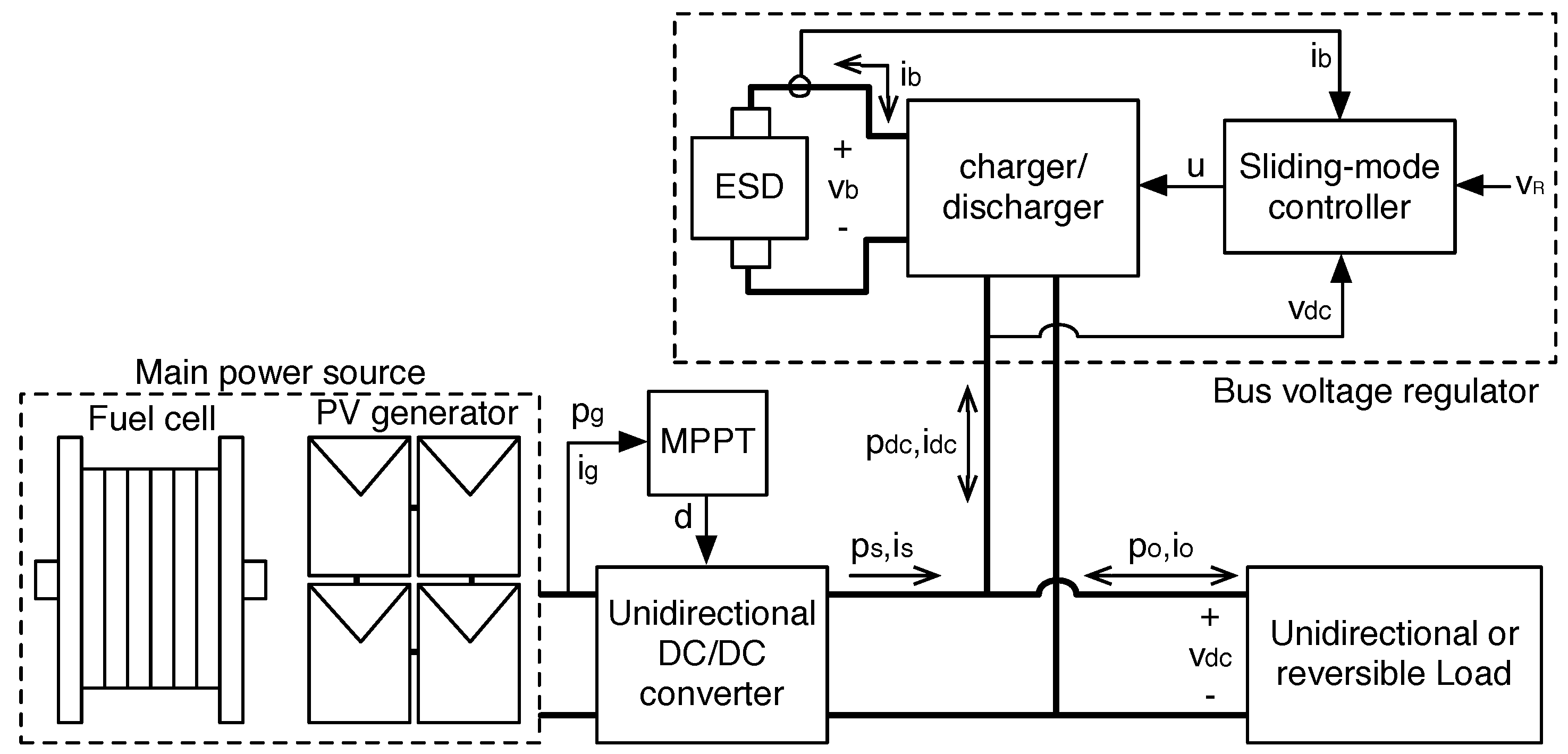
The use of renewable energy sources, or any other non-reversible source with limited bandwidth, requires the use of an additional Energy Storage Device (ESD) to store and release energy depending on the generator and load profiles: for example, slow sources (e.g., fuel cells) require ESD to support fast load transients [
17], or non-predictable sources (e.g., photovoltaic panels) require ESD to support stand-alone loads during low irradiance conditions or nights [
8]. A common structure used for power systems based on renewable generators and ESD is presented in
Figure 1. This stand-alone power system has been extensively used in applications such as electric vehicles [
27,
28,
29,
30,
31,
32,
33], irrigation systems [
34,
35], heating systems [
36], energy supply systems for telecommunication equipment [
37,
38,
39],
etc. The system considers the renewable energy source, e.g., photovoltaic panel or fuel cell, connected to an unidirectional DC/DC converter whose purpose is to operate the renewable generator in its optimal conditions. In addition, a charger/discharger power converter interfaces the ESD with the DC bus. Such a charger/discharger controls the power flow exchanged between the ESD and the DC bus, and at the same time, it is in charge of regulating the DC bus voltage. The main advantages of this topology are: the capability of storing the energy-in-excess produced by the generator; the capability of releasing the stored energy when it is needed; and the impedance decoupling between the renewable source and the other elements, which enable to optimize the source operation.
Multiple solutions reported in literature adopt the previous topology. For example, the work in [
40] presents a power system based on a fuel cell and an ESD (supercapacitor and battery). In addition, a sliding-mode controller is used to regulate the bidirectional Buck-Boost converter with the aim of control the DC-bus voltage and the supercapacitor current. Moreover, the system includes a Boost converter to regulate the fuel cell, which is controlled with a PI structure to deliver a constant power flow without power peaks. However, this system does not include an optimization algorithm to improve the fuel cell operation, hence a fraction of the stored hydrogen could be wasted. Furthermore, the adopted sliding surface does not include the integral of the DC-bus voltage error, therefore it is difficult to guarantee null steady-state error in any condition.
Similar topologies have been used in automotive engine/battery hybrid power systems. An example is presented in [
41], which is based on a bidirectional DC/DC converter controller with a variable current limiter. Similarly, The work presented in [
42] proposes a three-level bidirectional converter for fuel-cell/battery hybrid power systems. In this case, the converter operates in both Buck and Boost modes controlled by a cascade of a voltage regulator and a current limiter.
In this kind of systems, one of the main challenges is to properly regulate the bidirectional power converter (charger/discharger) associated to the ESD: the controller must operate with both positive and negative power flows with minimum disturbances even at null power, the non-linear system model changes for both positive and negative current, the DC-bus voltage must be regulated in both conditions, among other problems. Linear controllers (PI, PID or lead-lag) can be designed to mitigate such a perturbations [
43]. However, the main problems associated with these kind of controllers are the reduction of the closed-loop bandwidth, and the requirement to use a linearized model of the system that makes impossible to ensure the same performance, or even stability, in all the operating conditions [
44,
45,
46]. Therefore, as reported in [
40], the sliding-mode control technique is a useful alternative to ensure stability in any operation condition, which is mandatory for a safe load operation.
This same approach is reported in [
47], which uses a sliding-mode controller to regulate a bidirectional quadratic-Boost converter intended to connect DC sources, e.g., photovoltaic panels, fuel cells, battery banks and wind turbines, to an inverter with Maximum Power Point Tracking (MPPT) capabilities. This sliding-mode controller defines four surfaces selected by means of hysteresis comparators, which drives the power stage to behave as a programmable power source to emulate the power
vs. voltage (P-V) curve of a photovoltaic panel. Hence, any source could be connected to a photovoltaic MPPT inverter.
Most control systems based on sliding-mode include in the sliding surface the error of one, or multiple, system states [
22,
48], e.g., capacitors voltage or inductors current. Moreover, other sliding-mode controllers adopt more complex sliding surfaces: for example, the work reported in [
49] propose a sliding surface formed by the output voltage error, and both the time integral and derivative of that error, this to stabilize a Buck converter with constant power load. Since such a surface can be written as a second-order differential equation, the mathematical analyses required to guarantee stability and desired performance are extensive despite the simplicity of the system model. Similarly, the controller reported in [
50] considers a sliding surface based on the output power error, hence it is a non-linear surface. This approach was used to provide constant power to the load and, at the same time, to reduce negative impedance instabilities. Other complex surface is presented in [
51], which is based on the output voltage error and the square of the output capacitor current in a Buck converter. This surface is intended to improve the settling time and steady-state error of the output voltage regulation.
This paper proposes an adaptive sliding-mode controller for the ESD charger/discharger to regulate the load voltage in any power flow condition. The solution considers the topology presented in
Figure 1 with the following characteristics: a renewable energy source connected to a power converter controlled by a MPPT algorithm to optimize the generator operation; a bidirectional power converter interfacing the ESD with the DC-bus; and a non-linear load requiring a stable DC-bus voltage. Moreover, the controller is designed to fulfill both steady-state and dynamic performance criteria, which are defined in terms of the safe margins required for the correct load operation. Finally, the sliding-surface is defined as a trade-off between complexity and performance.
The paper is organized as follows: the next section presents the structure of the DC-bus voltage regulator and its mathematical model. Later, in
Section 3, the sliding-mode controller is proposed and mathematically analyzed.
Section 4 deals with the design of the sliding-mode dynamic behavior to fulfill the load and DC bus operative restrictions, while
Section 5 introduces the adaptive laws and the proposed design procedure.
Section 6 and
Section 7 present both simulation and experimental results to validate the sliding-mode controller, the mathematical analyses and the proposed design procedure. Finally, the conclusions close the paper.
2. DC-Bus Voltage Regulator
The classical structure of stand-alone power systems based on renewable energy sources is presented in
Figure 1 [
52,
53]. This structure is composed by an energy generator, e.g., a fuel cell or PV generator, connected to a DC/DC converter controlled by a MPPT algorithm to optimize the operation of the power source. In addition, an ESD is connected to a charger/discharger system to manage the DC-bus and the ESD state-of-charge. This charger/discharger usually involves a bidirectional DC/DC converter, where the DC-bus is formed by the parallel connection of the DC/DC converters output. Finally, unidirectional or reversible loads are connected to the DC bus, hence such a bus must provide a regulated voltage depending on the load requirements.
Due to the low voltage operation commonly exhibited by renewable generators, and the medium-to-high voltage required by several commercial loads, the unidirectional DC/DC converter is designed with the boost topology to provide both simplicity and high voltage conversion range [
43,
54,
55]. In addition, the MPPT controller acting on the DC/DC converter is designed to optimize the operation of the renewable generator: for example, if a PV generator is used as the main source, the MPPT controller defines the duty cycle
d of the DC/DC converter to increment the PV power
generated [
43,
54]. Similarly, if a fuel cell is used as main generator, the MPPT controller regulates the DC/DC converter to decrement the input current
, which is proportional to the hydrogen consumption [
56,
57,
58]. Note that, in both cases, the output of the unidirectional DC/DC converter is not regulated, hence it provides a power profile
with a non-regulated current
. Therefore, the charger/discharger must be controlled to provide a stable voltage
to the DC-bus in concordance with the load requirements.
In agreement with the previous requirement, the ESD and the charger/discharger with its associated controller form the DC-bus voltage regulator. This system provides or absorbes the power difference between the renewable generator and the load. This bus voltage regulator enables the system to supply energy when the main power source is not able to cover the load profile, i.e., . Furthermore, the bus voltage regulator stores the energy when the load is not consuming, or when a regenerative load recovers energy (negative ), e.g., regenerative breaking in electrical vehicles. In conclusion, the bidirectional DC/DC converter behaves as a voltage source with a power profile equal to the positive or negative difference between the load and generator powers, i.e., with since must be regulated.
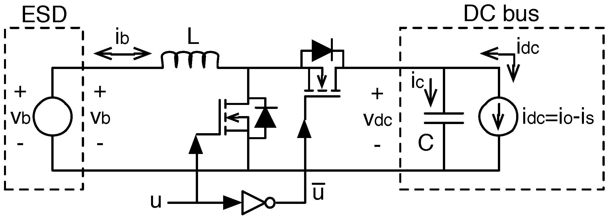
This paper adopts the bidirectional DC/DC converter presented in
Figure 2 to enable both positive and negative current flows from/to the ESD. That switching structure is designed to interface low ESD voltages
with DC-buses exhibiting higher voltages
,
i.e.,
. This is a common condition for systems that are based on low-voltage batteries or super-capacitors. In the electrical scheme of
Figure 2 the ESD is modeled as a voltage source with current
, while the DC bus is modeled by a capacitor
C and its associated current flow
. The switched differential equations that describe the system dynamics are given in Equations (1) and (2), where
u represents the MOSFET activation signal (
for ON state and
for OFF state). Such a model accurately describes the charger/discharger dynamics.
In conclusion, the main objective of the control system associated to this bus voltage regulator is to control the output voltage of the bidirectional DC/DC converter to guarantee stability. However, the non-linear nature of the bidirectional DC/DC converter makes impossible to guarantee the global stability using classical lineal control techniques, e.g., PI, PID or lead-lag controllers. Moreover, the output voltage of the converter must be regulated in both charge and discharge operation conditions (positive and negative power flows), which is not a trivial task for linear controllers. In the light of the previous conditions, the charger/discharger must be regulated by a non-linear controller to guarantee the global stability of the DC bus in any operation condition.
3. Sliding-Mode Controller Analysis
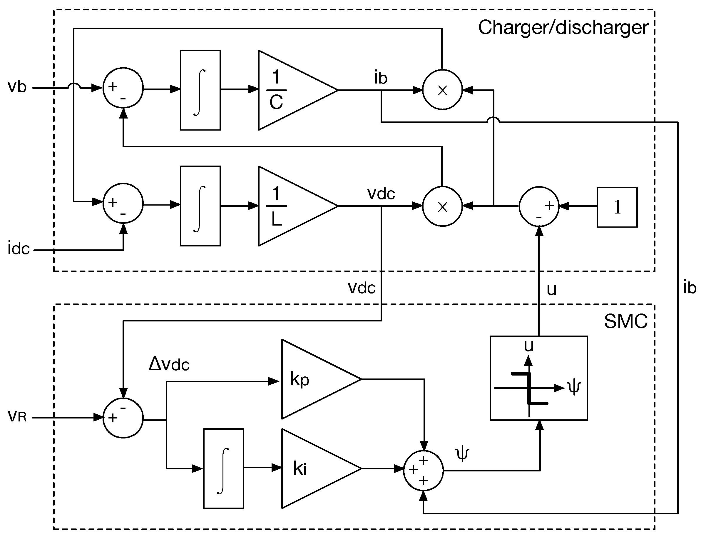
This paper proposes a sliding surface formed by the ESD current , the DC voltage error and the integral of the DC voltage error. In this way, the controller is able to detect the direction of the power flow (charge or discharge), given by the sign of , and the error in the DC voltage. The proposed switching function Ψ and sliding surface Φ are given in Equation (3), where represents the desired DC bus voltage (or reference) given by the load requirements, while and are parameters of the surface.
Figure 3 presents the block diagram of the sliding-mode control system, where the converter differential equations, in state-space representation, interact with the sliding-mode controller (SMC). The MOSFET activation signal
u is generated by an inverted-comparator centered in zero evaluating the switching function Ψ.
The derivative of the switching function is given in Equation (4), where represents the deviation of the DC voltage from the desired value. The reference is a constant value defined by the load requirements. Substituting Equations (1) and (2) into Equation (4) leads to Equation (5), which includes the binary control variable u.
Inside the sliding-surface,
i.e., if the sliding-mode exists, the conditions in Equation (6) are fulfilled [
59,
60,
61,
62], which in steady-state stand for
and
, hence a stable DC voltage equal to the desired value.
To guarantee the existence of the sliding-mode,
i.e., guaranteeing Equation (6), three conditions must be ensured [
59,
60,
61]: transversality, reachability and equivalent control. The transversality condition analyses the system controllability, the reachability analyses the ability of reaching the surface, and the equivalent control analyses the local stability. Therefore, the transversality condition must be fulfilled to enable the sliding-mode controller to affect the system dynamics. The reachability condition must be fulfilled to enable the controller to drive the system towards the desired operation condition. Finally, the equivalent control condition must be fulfilled to enable the system to keep trapped inside the sliding-surface. In the following subsections those conditions are analyzed in detail.
3.1. Transversality Condition
The transversality condition analyses the presence of the control variable in the derivative of the sliding-surface as given in Equation (7) [
60,
63]. In such a way, the fulfillment of Equation (7) ensures the ability of the sliding-mode controller to modify the system behavior.
Deriving Equation (5) with respect to
u leads to the following equation:
From such an expression three possible conditions are indetified:
,
i.e., null power exchange between the ESD and the bus;
,
i.e., charging the ESD from the bus;
,
i.e., discharging the ESD to supply the bus. From the first condition it is concluded that the transversality value is positive as in Equation (
9), which imposes the reachability conditions as described in [
60,
64]. Therefore, the transversality must exhibit the same sign in all the conditions to provide an unified analysis that ensures the existence of the sliding-mode. Moreover,
Section 3.4 will demonstrate that both
and
must be negative to guarantee a stable behavior of the system.
Then, also in the second condition the transversality must be positive, which in Equation (8) requires since , L and C are positive quantities. Similarly, in the third condition the transversality must be positive, which requires that condition Equation (10) be fulfilled. Then, such a restriction must be included in the design process of .
3.2. Reachability Conditions
The reachability conditions analyze the ability of the system to reach the surface [
60,
64]. In such a way, the sign of the transversality defines the reachability conditions: since
then a positive derivative of the switching function is obtained for
, while a negative derivative is obtained for
. For a negative transversality the relation is inverse.
Therefore, if the system is operating below the surface,
i.e.,
, the switching function derivative must be positive to reach the surface. Similarly, if the system is operating above the surface,
i.e.,
, the switching function derivative must be negative to reach the surface. Such conditions are mathematically described in Equation (11) [
60].
Replacing Equation (5) into (11), the following conditions must be guaranteed:
To further analyze such expressions, the power balance equations of the DC/DC converter (disregarding losses) given in Equation (14) must be used, in which d represents the converter duty cycle.
Using those relations, inequalities Equations (12) and (13) become:
The term
is positive since it corresponds to the transversality value, and
is required to guarantee a stable behavior of the system as will be explained in
Section 3.4. In addition,
could be zero, positive or negative:
stands for the desired
condition;
stands for an undershot
, e.g., a fast increment in the bus current; while
stands for an overshot
, e.g., a fast decrement in the bus current. Then, both Equations (15) and (16) must be analyzed for the three possible
conditions.
Then, both Equations (19) and (20) restrictions must be fulfilled to guarantee the reachability conditions. Such restrictions must be included in the design process of .
3.3. Equivalent Control Condition
The equivalent control condition analyzes the local stability of the system. In such a way, the conditions in Equation (6) must be achieved in the normal operation of the DC/DC converter,
i.e., switching the MOSFET state (ON or OFF) using the control variable
u. This means that
u most not be permanently in ON or OFF state. Therefore, the analog equivalent value of
u, denoted as
, must be constrained within the values of
u. Such a condition is mathematically expressed as follows [
63,
65]:
Replacing
u by
in Equation (5), and equating it to zero, leads to the following expression for the equivalent control:
Then, expressions for and are obtained in Equations (23) and (24), respectively. Such expressions are equivalent to Equations (12) and (13), hence fulfilling the reachability conditions also guarantee the equivalent control condition.
3.4. Sliding-Mode Dynamics
The existence of the sliding-mode ensures the fulfillment of the conditions previously described in Equation (6). In such a way, the sliding-mode dynamics are given by Equation (25), in time domain, and by Equation (26), in Laplace domain. Such expressions impose the closed-loop dynamics of the ESD current .
Then, the DC bus voltage dynamics,
i.e., Equation (2), is imposed by Equation (26). Moreover, since the sliding-mode controller drives the MOSFET signal
u, expression Equation (2) must modified to include the sliding-mode dynamics. To remove the switching condition from Equation (2) it is required to average the binary control signal
u over the switching period
T, which is known as the averaged model approximation [
66,
67]:
Then, considering that , the closed-loop dynamic behavior of the DC voltage is given by Equation (28).
Finally, by combining Equations (26) and (28) in Laplace domain, the complete closed-loop dynamic behavior of the bus voltage is given by Equation (29), which depends on the perturbations introduced by the bus current and the reference.
However, as pointed out before, the reference is a constant value imposed by the load characteristics, while the bus current depends on the operation conditions of the main generator and on the load power request. Therefore, the system given in Equation (30) is used in the following section to design the parameters and of the sliding-mode controller.
Finally, Equation (30) demonstrates that both and must be negative to guarantee stable sliding-mode dynamics, otherwise the equivalent dynamics will exhibit negative poles, i.e., an unstable behavior.
4. Design of the Sliding-Mode Dynamic Behavior
The closed-loop dynamics of the sliding-mode system, given in Equation (30), show that any persisten change on the DC bus current
will be compensated,
i.e.,
. However, the dynamic behavior of the bus voltage must be controlled to avoid large voltage undershoots that could turn-off the load, or large voltage overshoots that could destroy the load. Therefore, the sliding-mode dynamic behavior is designed in terms of the following performance parameters and conditions:
The DC-bus could experiment fast current perturbations due to both load profile and renewable source characteristics. For example, PV generators could exhibit fast current decrements due to shades projected by mobile objects [
68,
69]. On the other hand, the load could request fast current increments, as in the case of microprocessors [
70], while fuel cells are unable to provide those fast step currents [
71]. In the first case the DC-bus will be exposed to step-like current decrements, while in the second case the DC-bus will be exposed to step-like current increments. Therefore, the SMC design must consider step-like perturbations with magnitude
.
The DC-bus voltage must be regulated at the desired value with deviations lower or equal to . This means that the maximum acceptable overshoot (or undershoot) is equal to .
During a transient, the load requires that the DC-bus voltage be recovered to an acceptable band , around the reference voltage, with a maximum stabilization time .
Then, the following information is required to design the dynamic behavior of the SMC: the expected maximum DC-bus current perturbation , the maximum voltage deviation accepted by the load, and the safe band and maximum stabilization time required for the correct operation of the load.
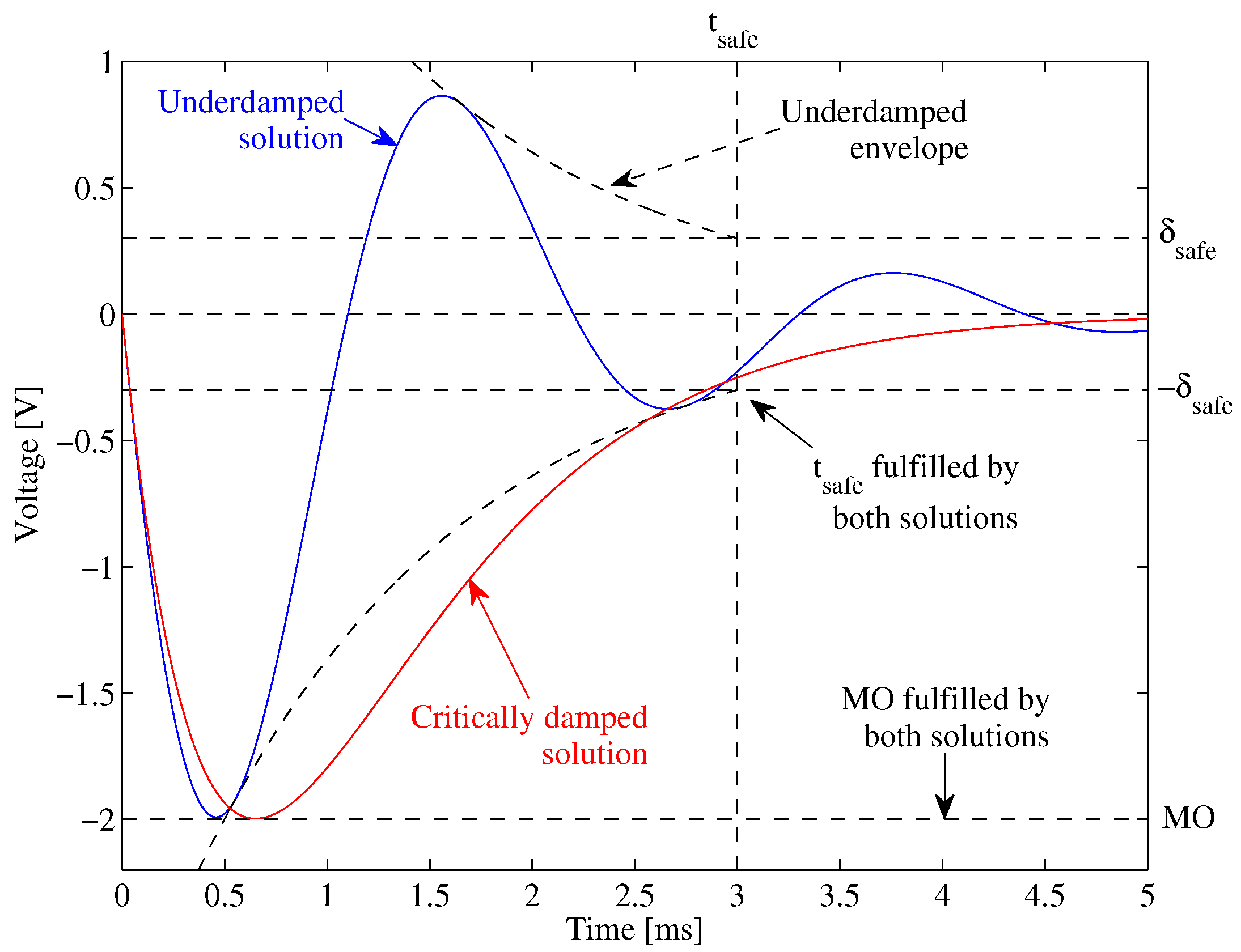
Since the previous design criteria are time-domain values, the time response of the DC-voltage, under the action of the sliding-mode controller, is calculated from the inverse Laplace transformation of Equation (30). Then, two possibilities are considered: an underdamped response and a critically damped response. The main characteristics of those options are:
Underdamped response: enable to reach faster the nominal voltage at the expense of oscillations around such a voltage. This dynamic response is suitable for loads very sensible to voltage drops but less sensible to voltage oscillations, e.g., microprocessors [
70].
Critically damped response: avoid oscillations around the nominal voltage at the expense of a longer delay to reach it. This dynamic response is suitable for loads very sensible to voltage oscillations but with larger tolerance to voltage drops, e.g., variable speed drives for DC series motors [
72].
This analysis does not consider an overdamped response since it does not provide any advantage over the critically damped response.
4.1. Underdamped Response
The step response of Equation (30), assuming values of and that leads to an underdamped time response, is given in Equation (31), where condition Equation (32) must be fulfilled to guarantee the underdamped behavior. Such a response considers the largest current transient expected from the DC-bus.
The highest DC-bus voltage deviation caused by such a transient corresponds to the maximum overshoot . The occurs when the voltage derivative is equal to zero as in Equations (33) and (34), which corresponds to the time given in Equation (35). Finally, the is calculated by evaluating Equation (31) in (35), which leads to the expression given in Equation (36).
Expression (36) can be used to design
and
to ensure a maximum voltage deviation equal to
. However, several loads require to restore the voltage within a safe range in a given time to avoid the turn-off of sensible circuits. That is the case of the Intel® Xeon® Processor W5590 configured to operate at 1.1V@100A, which after a current transient must operate at least at 0.99 V after a maximum delay of 25 ms [
70]. Similarly, exposition to long over-voltages could damage some loads such as the same Intel® Xeon® Processor W5590, in which overshoots cannot exceed 50 mV [
70]. Therefore, in general, the bus voltage must be driven within the safe limits
and
in, at maximum, the time interval
. Such a condition is commonly addressed by using the settling-time
criterion, but the traditional expressions for
are, in general, inaccurate and they could lead to controllers that provide an effective settling time longer than the expected one as discussed in [
73,
74,
75]. Moreover, the traditional
expressions provide inaccurate predictions for systems with a zero, e.g., Equation (30), as discussed in [
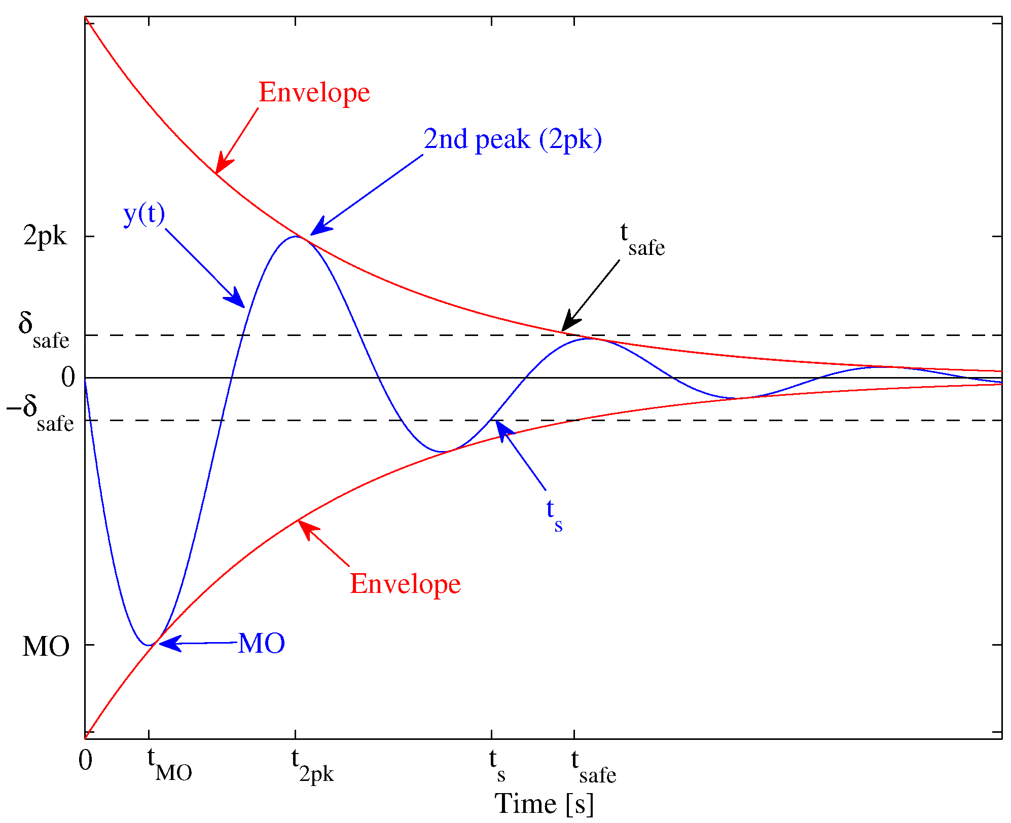
76]. Therefore, this paper proposes to design the sliding-mode controller using the envelope component of the system time response. To illustrate such an approach,
Figure 4 presents the time response of Equation (30), and its envelopes, for a positive step perturbation in the DC-bus current. In the figure it is observed the undershoot
occurring at
; while the system enters into the safe band
at the instant
. However, since
is difficult to predict due to the periodic oscillation, it is simpler (and safer) to predict the time
in which the envelope enters the safe band since
. Therefore, designing the controller on the basis of
ensures that the systems enters the safe band in a time lower or equal than the required one
.
The expression describing the envelope waveform is obtained by removing the sinusoidal component from Equation (31), leading to expression Equation (37), which is parameterized in terms of and .
Finally, expressions Equations (36) and (37) form a simultaneous non-linear equation system that must be solved to calculate and , so that the DC-bus voltage exhibits a maximum deviation for a DC-bus current perturbation , entering into the load safe band in the time . Moreover, and must fulfill the constraints Equations (10), (19) and (20), which are required for the existence of the sliding-mode, and constraint Equation (32), which is required for an underdamped behavior.
Such a constrained and non-linear equations system can be solved using numerical methods like Trust-Region or Levenberg-Marquardt [
77,
78], e.g., using Matlab fsolve function.
4.2. Critically Damped Response
The main disadvantage of the underdamped design is observed in
Figure 4: in addition to the larger voltage deviation
, the DC-bus voltage exhibits several additional oscillations. In fact,
Figure 4 highlights the second peak (2pk) of the voltage, which in this case has an amplitude of 52.3% of
; therefore the load must support a voltage drop of
and an over-voltage of
. After that, a third peak with an amplitude of 27.3% of
occurs, causing an additional voltage drop; this cycle is repeated for several additional peaks. Some loads, like variable speed drives for DC series motors [
72], are very sensitive to voltage oscillations, therefore for those cases it is desirable that the DC-bus voltage exhibits a low number of oscillations. It is impossible to avoid the voltage perturbation caused by the current transients, however it is possible to design
and
to impose a critically damped behavior, thus the bus voltage will exhibit only a single peak
. It must be point out that an overdamped behavior will not exhibit any advantage since they also provide a single peak
but with a longer safe time; therefore this paper deals only with the critically damped behavior.
The system Equation (30) must fulfill the condition in Equation (38) to have two equal and real poles, i.e., to produce a critically damped waveform. Then, the step response in such a condition to a current transient is given in Equation (39).
The maximum voltage deviation
occurs when the derivative of the time response is equal to zero as given in Equation (40). The time in which the
occurs is given in Equation (41)
The is calculated by evaluating Equation (41) in (39) to obtain Equation (42). In such a way, and are calculated from Equations (42) and (38), respectively, to ensure a maximum deviation , but none condition regarding the safe band and safe time are introduced.
Therefore, it must be verified that the time
required by this critically damped system to reach the safe band is lower, or at least equal, to the minimum time
required for the normal operation of the load. Such a condition is calculated from Equation (39) as follows:
Finally, the values of and must fulfill the constraints Equations (10), (19) and (20), which are required for the existence of the sliding-mode, and constraint Equation (43), which is required for the safe load operation.
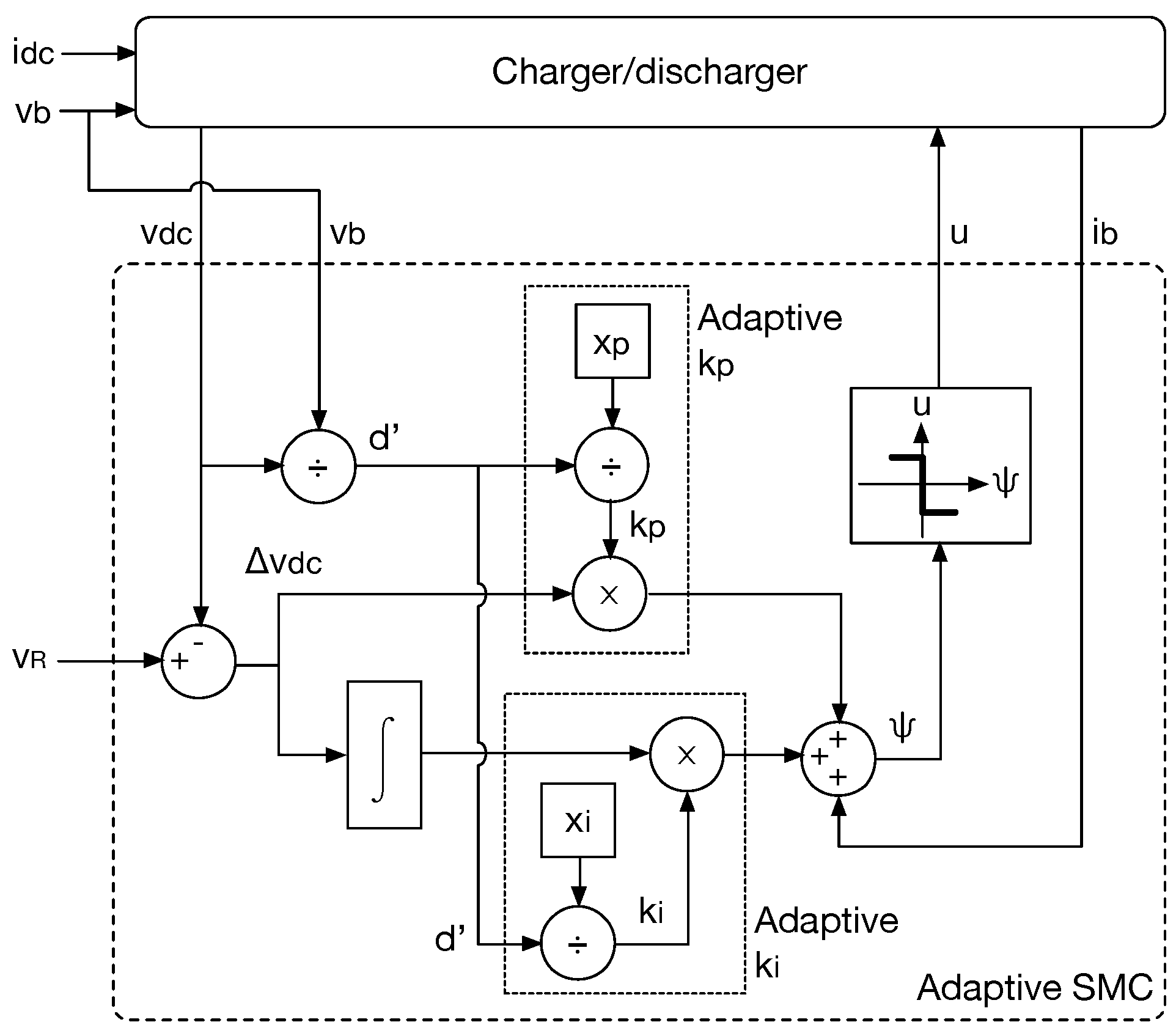
5. Controller Design and Operation
The previous sections provide equations to calculate and verify the SMC parameters and . However, those equations depend on the duty cycle d of the bidirectional DC/DC converter (charger/discharger), which changes depending on the values of the DC-bus and ESD voltages. Therefore, and must be continuously adapted to such changes on d, otherwise the conditions required for the existence of the sliding-mode could be not fulfilled, or the desired sliding-mode dynamics could not be achieved.
To address this problem, the equations to calculate and verify the SMC parameters must be normalized in terms of the duty cycle. Such a procedure was performed by defining the variables and to rewrite all the system equations, so that and are the unknown variables to be calculated instead of and .
In such a way,
and
are calculated off-line depending on the capacitance
C, the maximum DC-bus current perturbation
, the maximum voltage deviation
imposed to the DC-bus, the safe band
and the maximum time
imposed to reach that band. Then, the sliding-mode parameters are adapted on-line as described in
Figure 5:
and
. Hence, this solution is an adaptive sliding-mode controller (Adaptive SMC).
5.1. Normalized Equations for the Sliding-Mode Controller (SMC)
The normalized equations for the sliding-mode constraints and parameters are obtained as follows.
5.1.1. Constraint Equations
Constraints Equations (10), (19) and (20) must be fulfilled to guarantee the existence of the sliding-mode. Such restrictions, in terms of
and
are:
To guarantee that and fulfill such constraints, those expressions must be evaluated in the worst-case conditions for the DC-bus and ESD voltages and currents.
5.1.2. Underdamped Behavior Equations
The equations for imposing an underdamped behavior to the DC-bus voltage are given in Equations (34)–(37). Such expressions, normalized in terms of the duty cycle, are:
Then, expressions Equations (49) and (50) form a simultaneous non-linear equations system that must be solved to calculate and in terms of C, , , and .
An additional constraint, given in Equation (32), must be fulfilled to guarantee the underdamped behavior. The normalized version, in terms of and , is given in Equation (51).
5.1.3. Critically-Damped Behavior Equations
The equations for imposing a critically damped behavior to the DC-bus voltage are given in Equations (42) and (38). Such expressions, normalized in terms of the duty cycle, are given in Equations (52) and (53). Moreover, it must be verified that the time taken by the bus voltage for reaching the safe band is lower or equal that the time required for a normal operation of the load. Such a verification is described in Equation (43), and its normalized version is reported in Equation (54).
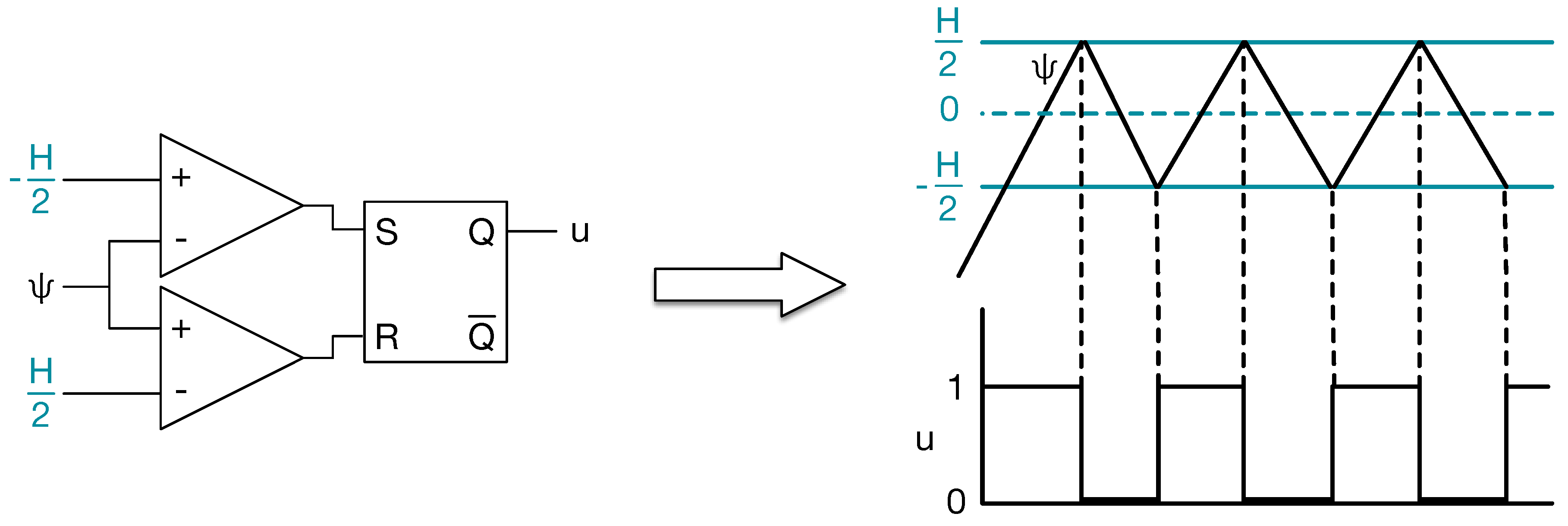
5.2. Switching Frequency
The zero-centered inverted-comparator used in the scheme of
Figure 5 to generate the MOSFET signal
u must be designed in terms of the switching frequency restrictions of the MOSFET used for the implementation. Therefore, sliding-mode controllers for DC/DC converters are commonly implemented using hysteresis comparators to constraint the switching frequency according to the physical limitations [
79,
80]. This paper adopts such a solution, in which the sliding function given in Equation (3),
i.e.,
, is modified as in Equation (55), where
H represents the width of the hysteresis band. The circuital implementation of Equation (55) is presented in
Figure 6, which is constructed with a Flip-Flop S-R and two classical comparators to generate the control signal
u. Moreover, the figure also presents the steady-state waveform of the switching function produced by the circuit.
In steady-state
, hence the switching function can be described as
, where
represents the switching ripple of the DC-bus voltage and
is a constant value. Therefore, the magnitude
H of the variation of Ψ depends on
and on the magnitude of the variation of
, which in the scheme of
Figure 2 corresponds to the switching ripple
of the inductor current. From the analysis of
and
derivatives, using Equations (1) and (2), it is noted that the maximum value of
ripple coincides with the minimum value of
ripple. Therefore, the magnitude of the oscillation in Ψ is
.
The magnitudes of the switching ripples, calculated from Equations (1) and (2) as reported in [
66,
67], are
and
, where
represents the switching frequency of the DC/DC converter. Then,
H is calculated from Equation (56) to limit the switching frequency to the value achievable by the MOSFET used in the implementation, it also depending on the inductance and capacitance of the charger/discharger, the maximum voltage supported by the ESD, the minimum voltage allowed to the DC-bus, and the maximum current injected from the DC-bus,
i.e., negative
. The last condition is due to, for a constant
H value,
is higher for negative bus currents as concluded from Equation (56).
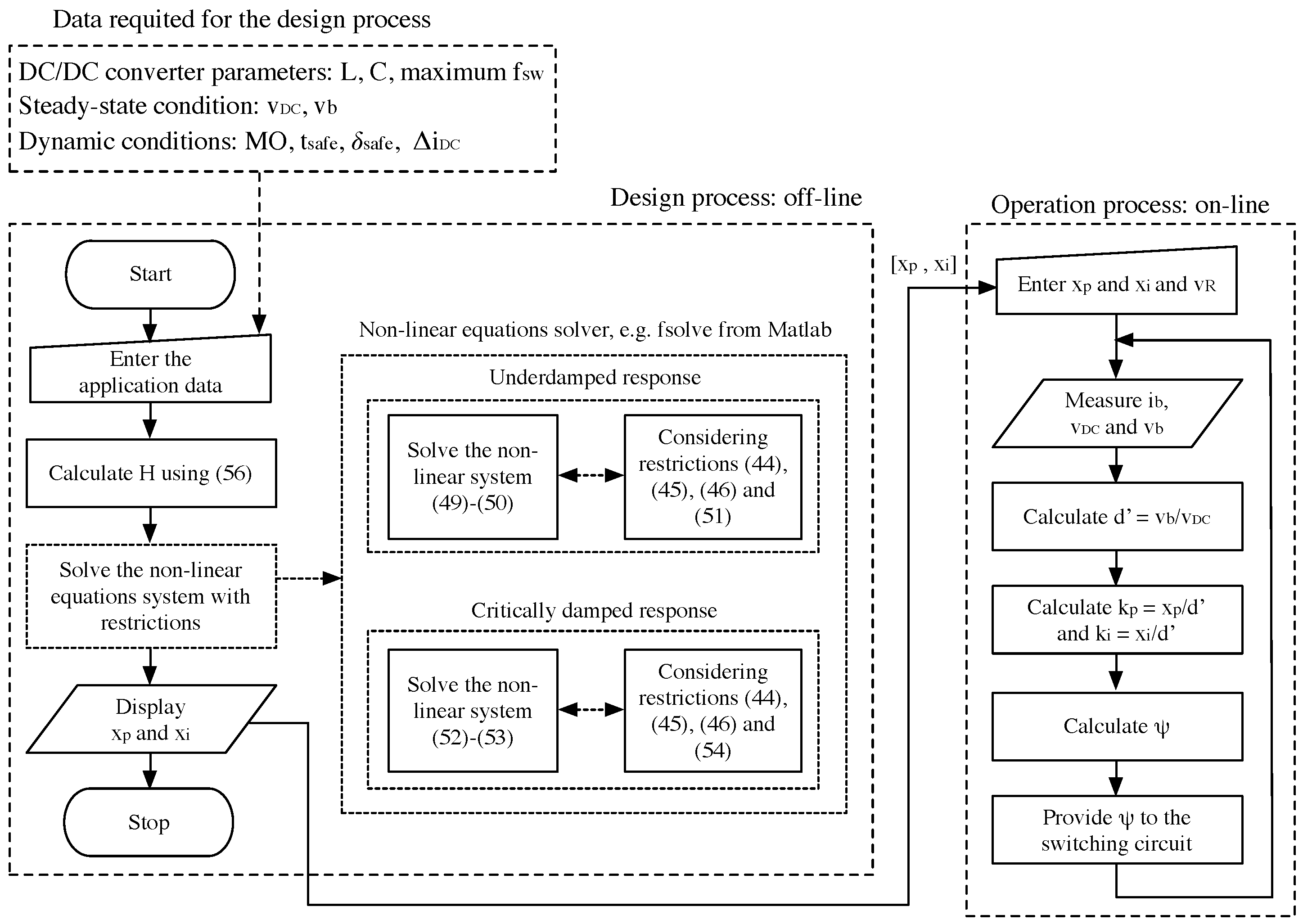
5.3. Summary of the Design Procedure and Operation
The design of the SMC is performed to fulfill both steady-state and dynamic conditions. The steady-state conditions are determined by the nominal DC-bus voltage and ESD voltage, which must be know. The dynamic conditions are: a maximum voltage deviation in the DC-bus, a safe band for normal operation , a maximum stabilization time to enter into the safe band after a perturbation, and a maximum bus current perturbation . In addition, the parameters of the DC/DC converter are needed, namely the capacitance C, inductance L and the maximum switching frequency .
The procedures to design and operate the SMC are described in the flowchart of
Figure 7. The design procedure is performed off-line, calculating first the hysteresis band
H. Then,
and
are calculated for the type of dynamic response that is best for the particular application: underdamped or critically damped behavior. Such a procedure is performed using a restriction-based solver for non-linear equation systems, e.g., fsolve from Matlab. It must be noted that, depending on the dynamic parameters
,
,
and
, the system of non-linear equations could not have real solutions for
and
. This means that the SMC is not able to guarantee those simultaneous constraints. That condition could be addressed using two possible solutions: first, the dynamic parameters could be relaxed, e.g., increasing
,
or
; and second, the dc/dc converter could be modified, e.g., increasing C for reducing
.
The operation procedure is performed on-line, calculating the complementary duty cycle to adapt and for the particular operation conditions. Such adaptive parameters are used to calculate the switching function Ψ, which is provided to the switching circuit to generate the MOSFET control signal u. This operation procedure cloud be performed with analog circuitry or in a digital processor.
6. Simulation Results
This section illustrates the design of the sliding-mode controller for the charger/discharger using the following parameters and conditions:
Bidirectional DC/DC converter with the following parameters: H and F. Moreover, the DC/DC converter is designed to support maximum voltage and current levels equal to 50 V and 10 A, respectively. Therefore, the converter supports a maximum load power of 500 W.
ESD nominal voltage V and DC-bus nominal voltage V.
Maximum DC-bus current transient: steps A.
Maximum voltage overshoot (or undershoot) to prevent load or DC/DC converter destruction or turn-off: V V, V].
Safe band for normal load operation: V V, V].
Maximum time to enter into the safe band after a transient: ms.
Maximum switching frequency: kHz.
The previous values were used to parameterize the equations described in the flowchart of
Figure 7. To illustrate both underdamped and critically damped solutions, two sets of parameters were obtained using the non-linear solver fsolve from Matlab:
and
. The first set of parameters was obtained using the underdamped equations, while the second set was obtained using the critically damped equations.
For the underdamped solution and , where the general restrictions Equations (44)–(46) are fulfilled: , and . Moreover, restriction Equation (51), which grants the underdamped behavior, is also fulfilled: .
Similarly, for the critically damped solution and , where the general restrictions Equations (44)–(46) are also fulfilled: , and . Moreover, restriction Equation (54) is also granted: ms ms.
Figure 8 presents the Matlab simulation of the equivalent sliding-mode dynamics using both solutions. Those simulation results show the accurate limitation of the maximum voltage deviation to
V for a current transient of
A. Moreover, the fulfillment of
ms is also verified. This simulation puts in evidence the difference between both solutions: the underdamped approach reaches faster the vicinity of the nominal DC-bus voltage, oscillating around such a value; instead the critically damped approach does not oscillates, hence it reaches the nominal voltage in a longer time. However, both solutions enter into the safe time almost at the same time, both respecting the design constraint
. Therefore, both solutions fulfill the design requirements, hence the selection of one of them depends on the specific load requirements as previously discussed in
Section 4.
The charger/discharger non-linear circuit was implemented in the power electronics simulator PSIM following the scheme previously presented in
Figure 2, and the adaptive sliding-mode controller was implemented following the structure given in
Figure 5, which corresponds to the online process described in the flowchart of
Figure 7. That algorithm was implemented in C language into a C-block of PSIM. Moreover, to simulate the processing of the SMC into a real digital device, the interaction of the C-block with the DC/DC converter and the hysteresis comparator was performed by means of Analog-to-Digital Converters (ADC) and a Digital-to-Analog Converter (DAC), which were simulated using quantization blocks of 12 bits with a sampling frequency of 1 MHz. In addition, the hysteresis band was designed using Equation (56) to ensure a switching frequency lower than
kHz, obtaining
. A slightly higher
was used to include a small safe margin.
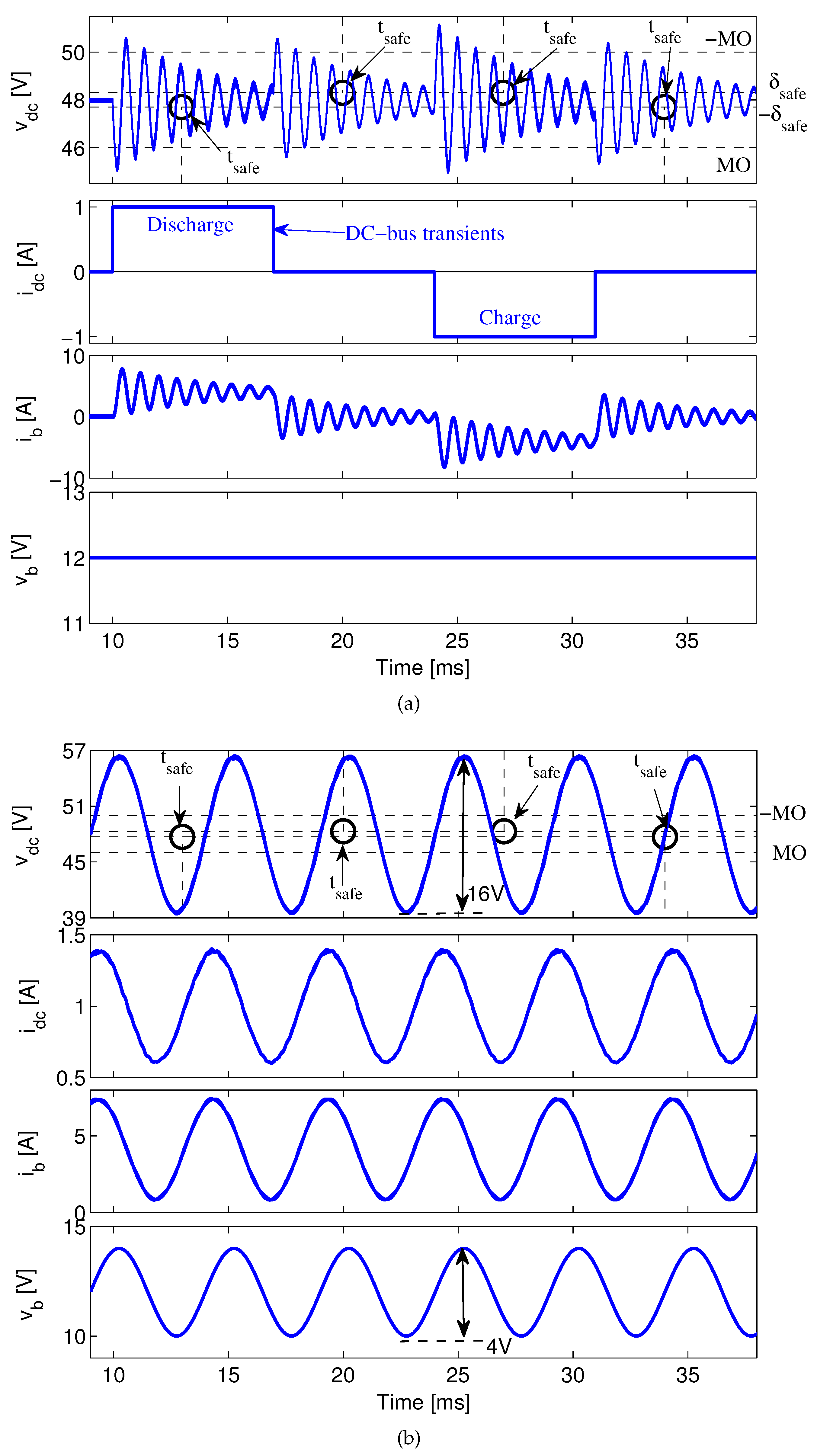
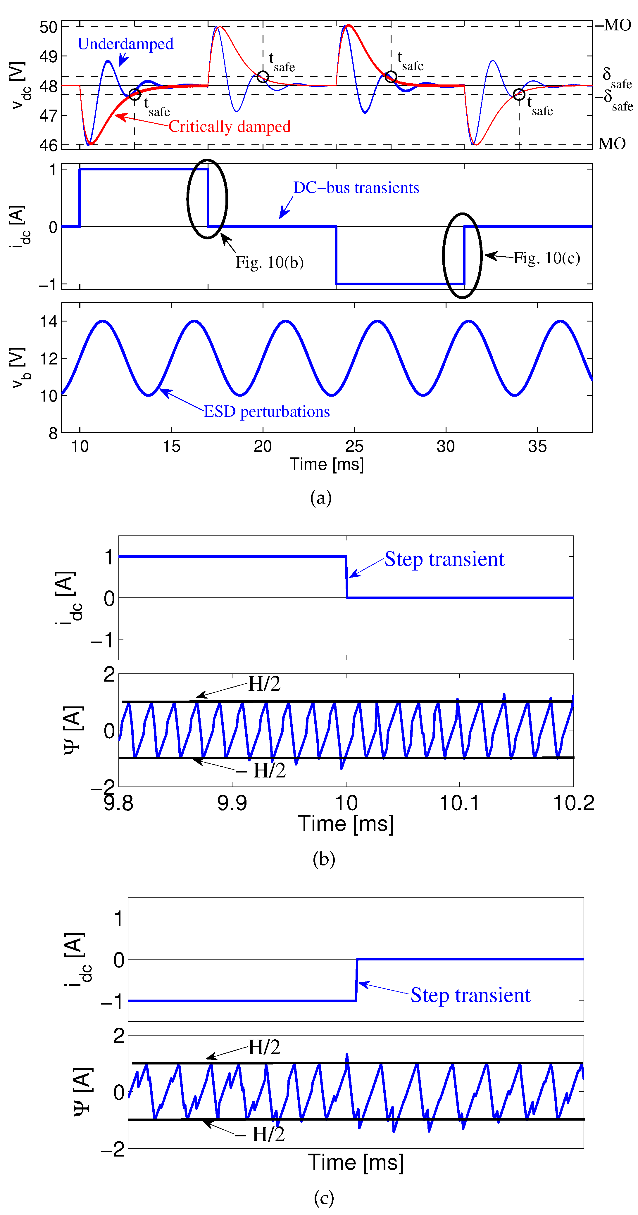
The electrical scheme was simulated using the two sets of parameters calculated for the SMC,
i.e., the underdamped parameters and the critically damped parameters, to validate the sliding-mode dynamics predicted in
Figure 8. Those electrical simulations are presented in
Figure 9a, where step current transients in the DC-bus are considered for both discharge (
A) and charge (
A) conditions. Moreover, the simulations also consider a
% sinusoidal perturbation at the ESD voltage
(
V oscillation around the nominal
V). It must be noted that such a perturbation is stronger in comparison with the variation of a battery voltage caused by normal operation of stand-alone power system based on renewable energy sources [
28,
40] or more general applications [
81], however this exigent perturbation is used to illustrate the robustness of both underdamped and critically damped sliding-mode controllers to variations in the ESD voltage.
The simulations confirm that both controllers are able to constrain the maximum voltage deviation to
V for current transients of
A. Similarly, both controllers guarantee that the DC-bus voltage enters the safe band within the imposed limit
ms. Moreover, the theoretical switching frequencies calculated from Equation (56) present errors below 1% with respect to those circuital simulations for
A,
A,
A] with
Hz,
Hz,
Hz], respectively. Finally,
Figure 9a also shows the battery current
for both cases, where the charge and discharge conditions of the battery are observed.
Figure 9b,c present the waveforms of the switching function Ψ at both step-down and step-up transients, respectively, generated by the simulation of the critically damped SMC. Those simulation results put in evidence the correct behavior of the SMC even with perturbations in both DC-bus and ESD: the switching function fulfills Equation (55),
i.e.,
, which guarantee the existence of the sliding-mode. Therefore, since the sliding-mode exists, the SMC is able to track the voltage reference rejecting perturbations in both the DC-bus and the ESD as observed in
Figure 9a.
Moreover, the electrical scheme of the charger/discharger was also simulated in open-loop,
i.e., with a constant duty cycle
, to illustrate the magnitude of the DC-bus perturbations caused by both load and ESD transients, which enables to evaluate the effectiveness of the SMC. In this case the charger/discharger operates with a boosting factor
.
Figure 10a shows the open-loop operation of the system for the
perturbations considered in
Figure 9a: the simulation put in evidence the requirement of the SMC to ensure the desired bus performance imposed by the load (
,
,
). Similarly,
Figure 10b shows the open-loop operation of the system for the
perturbations considered in
Figure 9a. However, in this case a resistive load equal to
is adopted to be in agreement with the constraints of the experimental devices used to validate this simulation. Moreover, the experimental device used to emulate the bus (BOP 72-14MG from Kepco) has a parasitic
network with
,
H and
F, respectively, which is also included in this simulation.
Figure 10b shows that the ESD oscillations are propagated to the DC-bus, generating a
V voltage oscillation out of the limits imposed by the desired bus performance. In conclusion, the open-loop operation of the charger/discharger could destroy the DC/DC converter since both perturbations produce voltages higher than the rated limit (
V), or even a shutdown or over-voltage damage to the load. Hence, the comparison between the open-loop (
Figure 10) and closed-loop (
Figure 9) simulations put in evidence the satisfactory rejection of perturbations provided by the proposed SMC.
Finally, the previous electrical simulations verify the correctness and accuracy of the proposed design procedure and adaptive structure for the sliding-mode controller to fulfill the imposed restrictions.
7. Experimental Validation
To experimentally validate the proposed design procedure and adaptive structure for the SMC, a proof-of-concept prototype was developed with the same parameters described in the previous section.
Figure 11a describes the prototype setup: the ESD was emulated using a four quadrant electronic source/load BOP 72-14MG from Kepco, which is able to provide and absorb power. Such an equipment was used to have the possibility of injecting perturbations in the ESD. Similarly, the main power source and load were emulated using another four quadrant electronic source/load BOP 72-14MG, which enables to impose positive and negative power profiles in the DC-bus.
The online adaptive process of the SMC was executed in a F28335 controlCARD from Texas Instruments programmed in C language, where Ψ is provided to the hysteresis comparator by means of the DAC MCP4822, which has a resolution of 12 bits and a sampling frequency of 20 MHz. The hysteresis comparator was implemented with the integrated circuit TS555, which provides the same circuital structure described in
Figure 6. However, the TS555 has the hysteresis centered in 2.5 V with band limits at 3.3 V and 1.6 V when the supply voltage is
V. Therefore, an additional amplification circuit was used to scale Ψ from 2 V to 1.7 V and to add an offset of 2.5 V, which corresponds to the scaled switching function
provided to the TS555. Then, the output of the TS555,
i.e., the binary control signal
u, and its complement
, are provided to the driver HIP4081A, which drives both MOSFETS.
The ESD current is measured using a shunt-resistor
and the amplifier AD8210, which is designed to scale bidirectional current measurements. Then, the output of the AD8210, the ESD voltage and the DC-bus voltage are acquired by the controlCARD using the onboard ADCs, which have a resolution of 12 bits and a sampling frequency of 12.5 MHz.
Figure 11b presents the physical setup of the experimental system.
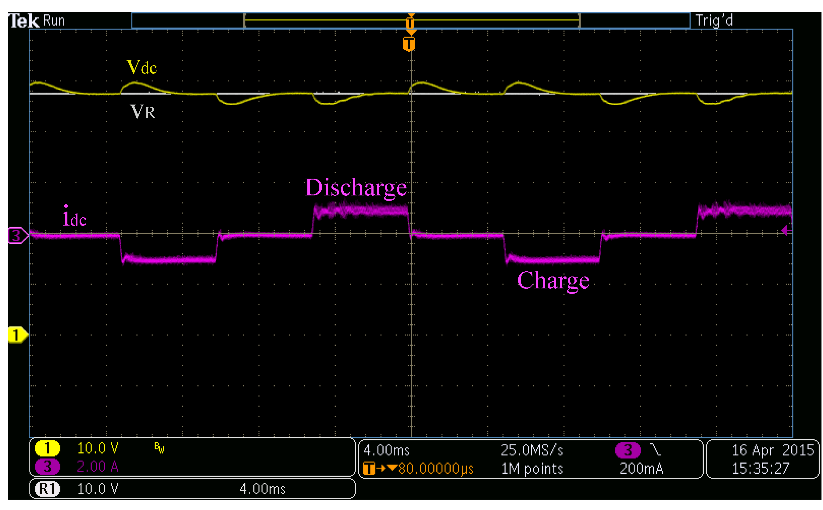
Two sets of experiments were carried out to test the performance of the SMC: a first one aimed at validating the SMC performance under step-like current transients in the DC-bus current, and a second one aimed at validating the SMC performance under perturbations in the ESD voltage.
The first experiment considers positive (discharge) and negative (charge) DC-bus currents with step-like transients. Therefore, this experiment has the same conditions considered in the simulations of the previous section. However, due to safety limitations of the BOP 72-14MG source/loads, it is preferable to avoid fast voltage oscillations in the DC-bus voltage, hence the experiment is only focused on evaluate the critically damped SMC.
Figure 12 presents the waveforms recorded for this experiment, which verify the satisfactory performance of the proposed solution: the DC-bus voltage is constrained to
V,
V] for step current transients of
A (due to the accuracy provided by the BOP 72-14MG), which represents an error of 3.8% with respect to the simulations presented in
Figure 9a. Such an error is mainly caused by the tolerances in the electronic elements, e.g., capacitor and inductor, hence introducing a safety margin in
, e.g., reducing it by 4%, will be enough to ensure the required operation conditions.
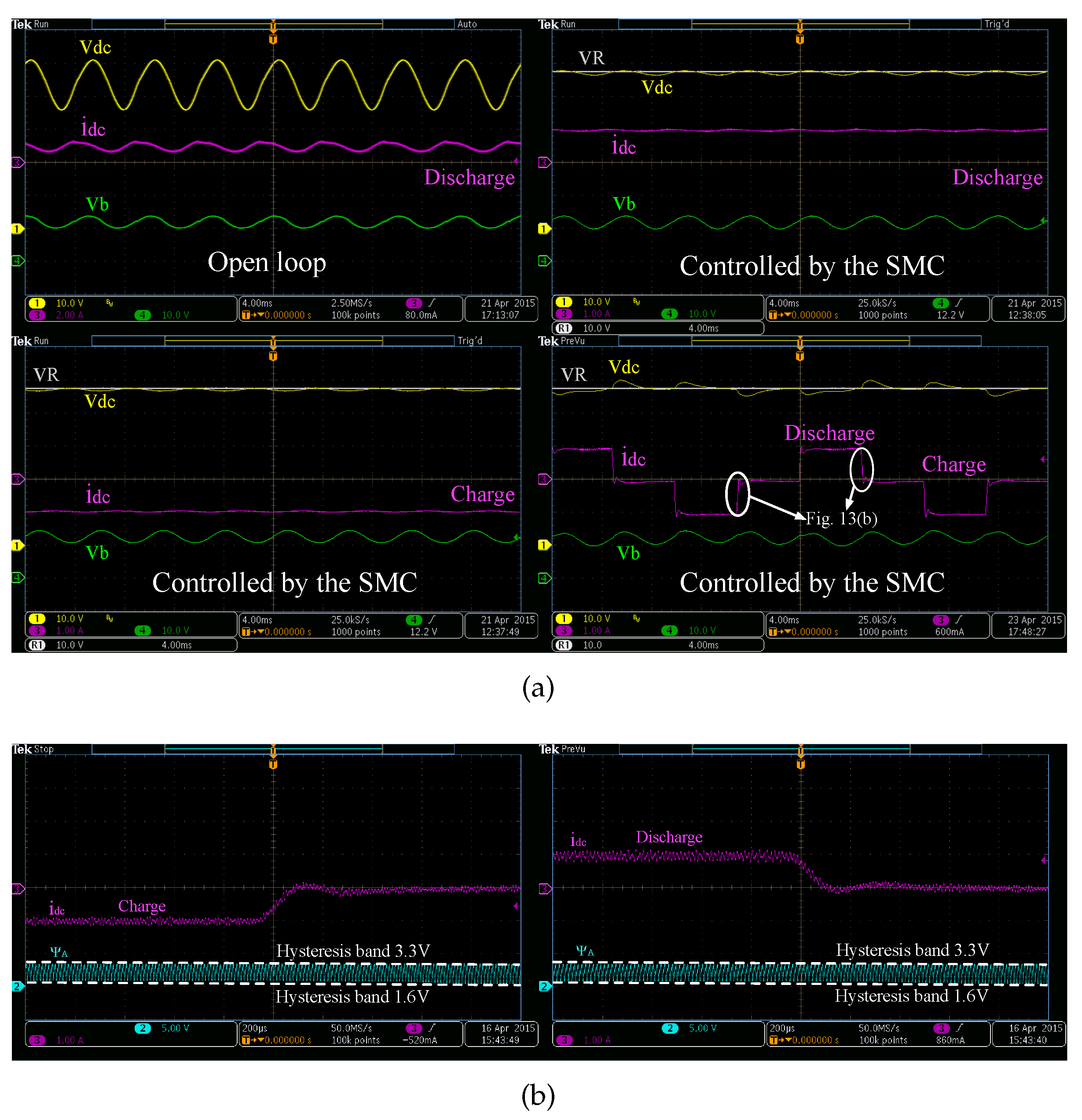
The second experiment considers the same ESD voltage oscillation presented in
Figure 10b to validate both open-loop and closed-loop simulations.
Figure 13a, at the top-left plot, verifies the large DC-bus voltage oscillations propagated in open-loop operation, which corresponds to the simulation presented in
Figure 10b. Moreover, the top-right experiment of
Figure 13a shows the satisfactory mitigation of the ESD voltage oscillations provided by the SMC in discharge condition (mitigated to 8.8% of the original amplitude). Similarly, the experiment at the bottom-left presents the SMC performance under the same ESD perturbation in charge condition (perturbation mitigated to 6.3% of the original amplitude). The experiment at the bottom-right shows the SMC performance under perturbations in both ESD voltage and DC-bus current, where again the DC-bus voltage is successfully regulated.
In addition,
Figure 13a presents the experimental scaled switching function for both step-up and step-down current transients. Such waveforms are in agreement with
Figure 9b,c: the switching function is constrained within the hysteresis band, hence the sliding-mode exists and the SMC is able to guarantee the required DC-bus behavior. Moreover, the waveforms in
Figure 13b, and
Figure 9b,c validate the circuit used to implement the switching control of
Figure 6 since the same results are obtained.
Finally, the simulation results presented in
Figure 9 validate the proposed design procedure and adaptive structure for the sliding-mode controller based in the surface (3). Moreover, the experiments reported in
Figure 12 and
Figure 13 validate such simulations results since the same behavior is obtained. Finally, those simulations and experiments demonstrate the correctness of the controller design and implementation.
8. Conclusions
This paper has presented a control strategy, based on the sliding-mode theory, to regulate a bidirectional DC/DC converter interfacing an ESD and a DC bus in a renewable power system. The control strategy provides a regulated DC bus voltage, ensuring global stability in any operation condition, despite of the non-linear nature the system and the bidirectional power flows. The controller is based on a sliding surface formed by the ESD current and both the DC voltage error and its integral, which enables to design the dynamic response of the DC bus voltage in agreement with the load requirements, where underdamped and critically damped responses are achievable.
The paper also provides detailed analyses of the sliding-mode conditions and proposes an easy-to-follow design process based on the load and DC bus operative restrictions, which are: maximum acceptable deviation of the DC bus voltage, the safe band for normal load operation, the maximum time acceptable to enter into the safe band after a perturbation, the maximum bus current perturbation and both the DC bus and ESD nominal voltages. However, the design equations and sliding-mode existing conditions depend on the converter duty cycle, hence they must be recalculated in each operation condition. To face this problem, those equations where normalized in terms of the duty cycle, providing new adaptive equations valid for the complete operation range. Hence, this solution is an adaptive sliding-mode controller.
The performance of this solution was evaluated by means of simulations made in both Matlab and PSIM, and with experimental data obtained in a proof-of-concept prototype. Both simulation and experimental results demonstrate the correctness of the adaptive sliding-mode controller, its mathematical analyses and the design process.
However, the proposed analyses consider one major simplification: both the converter equations and adaptive laws do not take into account parasitic losses. Without such a simplification the system and SMC equations are very complex and difficult to analyze, however a future paper could be dedicated to that particular topic to provide an improved design process.
Similarly, the proposed switching function has a relative degree 1, hence it can be implemented with a higher-order (second) sliding-mode controller as reported in [
82], e.g., using a twisting or super-twisting controller instead of the classical sliding-mode controller. Such an approach will enable to reduce the controller chattering, but at the expense of a much more complex mathematical analyses, which is an interesting topic for a future work. Moreover, the implementation of a twisting controller requires the measurement (or estimation) of the system state derivatives, or at least its sign, which increases the circuit complexity. This problem can be addressed by using estimation techniques, such as sliding-mode observers or Kalman filters. In contrast, the design of a super-twisting controller requires a first-order sliding surface, which produces an asymptotic behavior with a not finite-time convergence time [
83,
84,
85]. The solution of those open problems could lead to design new controllers with improved performance: reduced chattering and electromagnetic noise, higher robustness, among others.


