Review

Advancements in Inorganic Hole-Transport Materials for Perovskite Solar Cells: A Comparative Review

by
Johannes Zanoxolo Mbese
1,2
1
School of Pure & Applied Chemistry, Department of Chemical and Earth Sciences, Faculty of Science and Agriculture, University of Fort Hare, Alice 5700, South Africa
2
Energy, Material, and Inorganic Chemistry Research Group (EMICREG), University of Fort Hare, Alice 5700, South Africa
Energies 2025, 18(9), 2374; https://doi.org/10.3390/en18092374
Submission received: 8 February 2025 / Revised: 21 April 2025 / Accepted: 24 April 2025 / Published: 6 May 2025
(This article belongs to the Section A2: Solar Energy and Photovoltaic Systems)

Abstract

:
Single-junction perovskite solar cells (PSCs) have been one of the most promising photovoltaic technologies owing to their high-power conversion efficiencies (PCEs) of ~27% and the low-cost fabrication processes involved, which pay off significantly given their distinct structural characteristics. Recently, inorganic hole-transport materials (HTMs) such as nickel oxide (NiOx) have been developed and received considerable attention for use in OPVs due to their excellent thermal stability, low-cost materials, and compatibility with scalable deposition methods. Here, we summarize the recent progress on inorganic HTMs for PSCs, which can be divided into three categories: NiOx, copper-based compounds, and emerging new alternatives. The deposition method (sputtering, atomic layer deposition, or a solution-based technique) is one of the most important factors affecting the performance and stability of PSCs. Finally, we review interfacial engineering strategies, such as surface modifications and doping, which can enhance charge transport and extend a device’s lifetime. We also balance the benefits of inorganic HTMs against the key challenges in advancing to commercialization, namely interior defects and environmental degradation. In this review, we summarize the recent progress and challenges toward developing cost-efficient and stable PSCs with inorganic HTMs and provide insights into the future development of these materials.

1. Introduction

With rising energy consumption, environmental degradation, and the limited supply of fossil fuels, the global demand for sustainable and renewable energy has progressed drastically in recent years [1,2,3]. There are many approaches to producing alternative energy, but among them, solar energy is the most abundant, renewable, and environmentally friendly [4,5,6]. Silicon-based solar cells, the market-dominating photovoltaic (PV) technology, with their intrinsic cost-effectiveness and power conversion efficiencies (PCEs) of 27.0% for single-junction cells and greater than 33% for tandem cells [7,8,9], have set the pace in photovoltaics. However, littered with high manufacturing costs, inflexible substrates, and lengthy fabrication procedures, these technologies, although mature, are usually hindered by technological implementations [10,11,12]. Perovskite solar cells (PSCs) provide a promising approach, especially with their comparable efficiencies and low-temperature solution-based fabrication capability [13,14,15]. To date, the certified PCE of PSCs has surpassed 26% as of early 2025, with further improvements found through novel material design, interfacial engineering, and device architecture [16]. Perovskite materials have extraordinary optoelectronic properties, including large absorption coefficients, extended carrier diffusion lengths, and tunable bandgaps, all of which make these compounds promising next-generation PV materials [17,18,19].
Yet, a prominent challenge in PSC commercialization is device stability, especially under ambient conditions [20,21,22]. Some of the major components causing instability comprise organic materials used in the hole-transport layer (HTL)—like spiro-OMeTAD—which is often hygroscopic and thermally unstable [23,24,25]. Under these circumstances, inorganic hole-transport materials (HTMs) have emerged as a priority topic in research because of their improved thermal stability, chemical durability, and possible compatibility with large-scale processing methods [26,27]. This review presents a comparative and updated insight into the recent progress of inorganic HTMs for PSCs. Specifically, we concentrate on well-established materials such as CuI, CuSCN, Cu2O, and the broadly employed NiOx in conjunction with developing candidates [24,26,28]. We emphasize their material properties, energy level alignment, deposition methods, and suitability for normal and inverted PSC architectures [24,28,29]. This review also addresses interfacial engineering strategies and recent attempts to alleviate commercialization hurdles [23,24,30]. This work builds on recent findings in the literature to help clarify the important role of inorganic HTMs in advancing PSC efficiency and operational lifetime and define encouraging avenues for future work [14,24,30].

Role of Hole-Transport Materials (HTMs) in Perovskite Solar Cells

Hole-transport materials (HTMs), which serve as selective contact layers enabling the efficient extraction and transport of photogenerated holes from the perovskite absorber to an electrode, are crucial for PSCs [31]. Efficient wide-bandgap perovskite solar cells, high hole mobility, proper energy level alignment with the perovskite valence band, optical transparency in the visible range, and long-term operational stability are critical features of HTMs to be combined with high-power conversion efficiencies (PCE) [32]. The HTM is sandwiched between the perovskite layer and the back electrode in conventional PSC architecture, as shown in Figure 1. It performs the following three key roles: (i) facilitating fast hole extraction from the perovskite; (ii) preventing electron transport to the anode, which suppresses recombination losses; and (iii) ensuring that the interface remains stable, preventing perovskite degradation under environmental stressors [14,26]. For example, traditional organic HTMs such as spiro-OMeTAD have been most frequently employed in PSCs because of their simple solution processing route and better energetics. Nevertheless, these materials suffer from moisture sensitivity, low intrinsic conductivity, and thermal instability. Furthermore, they need expensive additives such as lithium bis(trifluoromethanesulfonyl)imide (Li-TFSI) and 4-tert-butylpyridine (tBP) that negatively influence the durability of the devices [28,33]. To address these disadvantages, inorganic HTMs are receiving major attention owing to their better thermal stability, inherent chemical stability, and suitability for high-throughput deposition methods [14,23]. Such materials provide additional advantages, non-doping operations, and stability under ambient processing conditions, which are critical for industrial applications.
One of the most promising inorganic HTMs is CuSCN, a wide bandgap (~3.6 eV), high-mobility (~10−2 cm2/V·s) material processible by solution techniques. Utilizing CuSCN as the HTM, PSCs have reported efficiencies of >15% with improved stability over time [34,35]. One other extensively researched material is CuI, displaying high conductivity and can be easily made at low temperatures. In addition, CuI-based devices suffer from interfacial recombination and low open-circuit voltage (Voc) from ineffective interface passivation [27,35]. Nickel oxide (NiOx) is among the most widely used inorganic HTMs in inverted (p–i–n) device architectures. It possesses good optical transparency, high valence band edge energy (~5.0 eV), and high chemical stability. Therefore, several recent studies have also examined PSCs incorporating NiOx layers that are either sputtered or physically deposited via atomic layer deposition (ALD), which were found to yield PCEs greater than 20%, highlighting that such material is highly useful for stable device architectures [36]. To achieve the highest efficiency, the HTM-HOMO level should be close to the perovskite valence band, allowing efficient hole extraction and minimal energetic losses. Moreover, HTMs should be smooth in surface morphology and adhere well to adjacent layers with fewer interfacial trap states, which contribute to device reproducibility [24,37]. For these reasons, transparency in the visible region and thermal stability well above 100 °C are critically important for all types of devices, especially multi-junction cells and outdoor environments. The rational design and choice of inorganic HTMs provide great opportunities to promote PSCs with high efficiency, great stability, and easy fabrication. We compare several established and emerging inorganic HTMs in terms of their structural, electronic, and interfacial properties and discuss their implementation in standard and inverted device architectures in the following sections.

2. Comparative Analysis of Inorganic HTMs for Perovskite Solar Cells

Inorganic hole-transport materials (HTMs) have many benefits compared to organic HTMs, such as thermal stability, long-term endurance, and compatibility with various fabrication methods. The following section outlines a series of the most commonly researched inorganic HTMs from the recent developments in PSCs, such as NiOx, CuSCN, CuI, Cu2O, V2O5, and CoOx, comparing their physical properties, device performance, and structural compatibility tabulated in Table 1.

2.1. Key Inorganic HTMs

Importantly, Table 1 offers a comparison of the key physical and electrical attributes of inorganic hole-transport materials (HTMs) that have been widely investigated to be adapted in PSCs, paving a path toward device architecture and processing conditions suitable for successful commercialization [14,23].
Of these materials, nickel oxide (NiOx) has attracted attention as a widely used HTM for inverted (p–i–n) PSCs due to its large bandgap (3.6–4.0 eV), deep valence band (~5.0 eV) and decent hole-selective property. Ideal thermal and chemical stability, together with the facility for using vacuum-based deposition techniques like sputtering and atomic layer deposition (ALD), enable devices with high reproducibility and scalability to be used [34,36]. NiOx HTLs have shown PCEs > 21% over large areas, along with device stability under continuous irradiation [14,38]. In contrast, common cationic Cu-based HTMs, such as CuSCN, CuI, and Cu2O, are often used in normal (n–i–p) structures, directly contacting with the metal electrode and requiring the efficient extraction of the holes generated on the upper perovskite surface [34,35]. These materials are appealing due to their high conductivity and compatibility with solution-processable techniques at low temperatures for the development of flexible and printable solar cells [39,40]. However, Cu-based materials have their limitations, especially for ambient stability and interfacial quality. For example, CuSCN is transparent and chemically stable, yet it is moisture-sensitive, leading to non-uniform film formation, which affects its fill factor (FF) and long-term stability unfavorably [34,41]. Despite being ultra-conductive, the CuI sometimes triggers interfacial recombination as well as lower open-circuit voltage (Voc), mainly attributed to poor band alignment and interface traps with certain perovskites [13,35].
Cu2O features high hole mobility, with some reports approaching >100 cm2/V·s, which is one order of magnitude higher than that of most organic HTMs [27,39]. Its relatively narrow bandgap (~2.0–2.2 eV), however, causes parasitic absorption and necessitates careful energy-level engineering to minimize Voc losses and ensure selective carrier extraction [38,39]. The properties of coordinate metal show high environmental tolerance, and the position of their wide valence band is ideal for hole extraction in inverted PSCs, which has led to the exploration of transition metal oxides like vanadium pentoxide (V2O5) and cobalt oxide (CoOx) as HTM candidates for solution-processed hole-transport layers [40,41]. However, these materials usually possess an inherently low conductivity and limited film-forming capabilities, making them suitable mostly as buffer layers or bilayer HTM structures, particularly with the addition of interfacial dopants or surface modifiers [13]. This survey study indicates that there is no ideal inorganic HTM that can outperform in all important metrics (i.e., energy-level alignment, conductivity, transparency, and stability) [14,27]. Thus, the choice of materials has to rely on specific device configurations, processing techniques, and applications. Often, trades are unavoidable, and the best HTM might rely more on interface fabrication and deposition control than the inherent material properties [13,36].

2.2. HTMs for Specific Device Architectures

To date, the introduction of inorganic hole-transport materials (HTMs) into perovskite solar cells (PSCs) must be flawlessly matched to the demands generated by chemistry and device architecture, both structurally and functionally [34,35,39]. There are two general device architectures for PSCs: normal (n–i–p) and inverted (p–i–n), and for each architecture, the optoelectronic properties of HTM should differ depending on the PSC structure [14,28,40].

2.2.1. HTMs for Normal (n–i–p) Architectures

In the standard (n–i–p) device architecture, the HTM is deposited onto the perovskite layer, which is then in direct contact with the metallic back electrode, typically gold (Au) or silver (Ag). In this regard, HTMs should possess superior film-forming characteristics, be upward-aligned on HOMO energy with respect to the perovskite valence band, and provide low interfacial recombination at the perovskite/metal interface [27,41,42]. Of these HTMs, copper(I) thiocyanate (CuSCN) is one of the most widely investigated elements and has shown considerable potential due to its large bandgap (~3.6 eV), high optical transparency, and compatibility with low-temperature, solution-based processing methods, in particular for substrates that may require flexible treatment [24,34,36]. Glabau et al. were the first to report on CuSCN-based PSCs that exceeded PCEs by over 16% with improved environmental stability [28,34,38]. Copper(I) iodide (CuI), despite also providing high intrinsic conductivity and rapid deposition, is subject to interface shunting and recrystallization losses, mainly in thin perovskite layers, and pinhole creation can enable direct contact with the electrode [23,35,43]. Hence, due to its use, it frequently needs extra passivation or a multilayer style for performance stability. Another compelling candidate in this regard is copper(I) oxide (Cu2O) due to its remarkably high hole mobility and significant light absorption in the visible region. On the other hand, its relatively narrower bandgap (~2.0–2.2 eV) increases the risk of parasitic absorption and requires stringent energy-level alignment strategies to mitigate Voc losses [39,40]. In addition, its surface chemistry and compatibility with perovskites require meticulous design interface engineering. Doped Cu-based HTMs (e.g., CuSCN:Ag, CuI:Na) with core–shell structures have been proposed to effectively mitigate interfacial losses due to improved coverage, less recombination, and tunable energy alignment [28,38,44].

2.2.2. HTMs for Inverted (p–i–n) Architectures

In inverted (p–i–n) PSCs, the HTM is directly deposited as the first active layer onto the transparent conducting oxide (TCO) layer (e.g., indium tin oxide (ITO) and fluorine-doped tin oxide (FTO)) [14,45,46]. The HTM in this setup must exhibit thermal and chemical stability with regard to perovskite deposition, low-temperature processability, and effective, selective hole extraction at the TCO interface [27,37,47]. Nickel oxide (NiOx) is the most popular inorganic HTM for this context due to its deep valence band (~5.0 eV), wide bandgap, and excellent optical transparency [14,48,49]. It can be deposited through solution processing, sputtering, or atomic layer deposition (ALD) [42], and recent advancements in terms of surface passivation and doping (e.g., Mg, Cu, Li) have led to improved conductivity and compatibility with perovskite films [24,50]. Besides NiOx, vanadium pentoxide (V2O5) and cobalt oxide (CoOx) are also being investigated due to their chemical stability and high work functions, facilitating hole extraction and promoting interface stability [40,41,51]. However, these materials typically have low intrinsic hole mobility, requiring interfacial dopants or bilayer buffer strategies to enhance charge transport and reduce recombination [27,41,42].

2.2.3. Current Trends in HTMs–Device Integration

Recently, new strategies of HTM design have been developed with encouragement toward the efficiency, scalability, and reliability of devices [24,36,49]. To improve the interfacial selectivity and minimize energy loss in charge extraction layers, graded or gradient-layer HTMs with spatially varied band alignments are also under development [16,52,53]. The key physical, electrical, and thermal properties of prominent inorganic HTMs are shown in Table 2. Synergistic advantages such as energy-level alignment, film morphology, and chemical passivation are associated with bilayer HTL systems that consist of an inorganic HTM and ultra-thin interlayers (for TiO2, MoO3, or organic modifiers) [27,37,54]. For commercialization, HTMs that are compatible with scalable deposition techniques, i.e., blade coating, slot-die coating, spray pyrolysis, and ALD, are increasingly being focused on, owing to their manufacturable nature for large-area and roll-to-roll technological applications [24,49,55].
The essential physical and electrical properties of leading inorganic hole-transport materials (HTMs) used in PSCs are listed in Table 2 as a comparative summary. Of these, NiOx is favored for its broad bandgap (3.6–4.0 eV), moderate hole mobility, and exceptional thermal and chemical stability, which renders it advantageous in inverted (p–i–n) perovskite topologies [13,14,23]. On the other hand, owing to their favorable conductivity and solution processability, Cu-based materials, including CuSCN, CuI, and Cu2O, are used in normal (n–i–p) architectures [34,35,38]. However, their performance is usually influenced by their surface roughness, susceptibility to ambient environments, and insufficient long-term stability if not surface-passivated or embedded in composite structures. Cu2O has an incredibly high hole mobility (as high as 256 cm2/V·s), but its smaller bandgap could induce parasitic absorption, and its misalignment with common perovskite absorbers would require interface tuning [27,39]. While V2O5 and CoOx exhibit stability and environmental tolerance, their poor conductivity requires doping elements or building layered architecture on electrodes to achieve enhanced performance [40,41]. This comparative perspective illustrates that no single inorganic HTM is universally superior and that the material choice must integrate performance parameters as well as processing and structural characterizations.

2.2.4. Tabular Comparisons: HTM–Device Architecture Matching

Table 3 aligns the HTMs to their compatible device architectures, as well as various deposition techniques and their peak PCEs. NiOx, particularly in inverted PSCs, provides large PCEs (>21%) and has strong thermal stability, particularly when deposited via sputtering or atomic layer deposition (ALD) [14,27,36]. CuSCN has shown itself to be effective in normal structures due to its wide bandgap (~3.6 eV), proper energy-level alignment, and transparency [34,38].
CuI has good processability and is cost-effective but may have poor interfacial passivation, potentially leading to recombination losses in the absence of extra interlayers [35]. Cu2O, when used in normal architecture, provides high mobility, but stable band alignment would need to be achieved through tuning surface states and interfacial layers to suppress chemical reactivity [27,39]. Other emerging HTMs (e.g., V2O5 and CoOx) are compatible with flexible inverted devices and may enable tandem cell integration, but they usually have rather low hole mobility, requiring further optimization [40,41]. These results underline the necessity of architecture-specific material-engineering approaches aimed at both maximizing charge extraction and reducing interfacial losses in a hybrid–organic system that is strongly hierarchy-driven.

2.2.5. Tabular Comparisons: Deposition Techniques and Scalability

Deposition Techniques: Owing to the different functionalities of 2D materials, various deposition techniques are important. Table 4 compares the deposition techniques along with their scalability, compatibility with other materials, and the quality of the films.
We demonstrate that vacuum-based methods like sputtering and ALD are being broadly adopted to obtain high purity and defect-free HTM films for NiOx and Cu2O, promoting the high efficiency of PSCs and tandem structures [14,27,36]. These techniques afford a tight control of thickness and uniformity but at a higher expense and lower throughput. Solution-based methods, such as blade coating, slot-die coating, etc., and related methods, such as electrodeposition, have drawn much attention for their low cost and compatibility with yield and flexible die. The electrodeposited CuSCN and sol–gel NiOx films made by these methods have performed very well, and reproducibility has improved significantly [24,34,38]. Moreover, both blade coating and slot-die coating allow the fabrication of HTM layers at high speeds and continuously under ambient conditions, which is well-suited for roll-to-roll processing, which is a main requirement for commercialization [23,24]. More recently, blade-coated NiOx HTLs have been shown to achieve >18% PCEs when combined with passivation strategies and to be highly air-stable [24]. These results show that the scalability of HTMs is attributable as much to the method of deposition as to the material itself, and hybrid processing strategies may provide a route to balance performance and manufacturability.

2.3. Deposition Techniques for Synthesizing Inorganic HTMs

The radar plot demonstrates the intrinsic trade-offs that guide the selection of inorganic hole-transport materials (HTMs) in perovskite solar cells (PSCs), which are determined by parameters like charge mobility, environmental stability, transparency, and process compatibility [14,23]. The visualization of trade-offs across six key criteria of the radar plot are stability, hole mobility, conductivity, band alignment, scalability, and transparency, which are displayed in Figure 2. Out of the studied candidates, Cu2O demonstrates excellent charge carrier mobility, with hole mobility exceeding the 100 cm2/V·s reported, which allows for fast hole extraction and lower resistive losses, although its inefficient transparency and small area of fabrication limits its potential [39,52].
The values of pairs agree well (on a relative scale ranging from 1 to 10, established according to a hybrid of experimental data and literature reports) and allow for a fair comparison to be made across the six fundamental material properties that we specifically examine in this work: stability, hole mobility, conductivity, band alignment, scalability, and transparency. This feature facilitates an understanding of the images presented and, thus, aids in the comparative study of inorganic HTMs in PSCs. NiOx demonstrates exceptional stability and energy alignment, while Cu2O offers superior hole mobility. CuSCN and CuI provide high conductivity and processability, whereas V2O5 and CoOx exhibit environmental robustness but require the enhancement of conductivity. Nickel oxide (NiOx) is a well-investigated HTM utilized in several inverted (p–i–n) configurations that is known for its chemical and thermal stability as well as favorable band alignment, with the perovskite valence band contributing to the low-voltage drop and high-efficiency of devices as well as long-term operational stability [27,36]. Moreover, its tunable nature via doping (e.g., Cu or Li) and compatibility with scalable deposition techniques (e.g., atomic layer deposition (ALD) and sputtering) further boost its attractiveness for commercialization [28,41]. Copper(I) thiocyanate (CuSCN), which possesses a wide bandgap (~3.6 eV) coupled with a high degree of hole selectivity, presents an advantageous balance between optical transparency and transport properties. Notably, this results in a favorable property that makes them suitable for ambient-condition low-temperature solution-based processes such as spin-coating and electrodeposition [34,38]. CuSCN-based devices have also exhibited high power conversion efficiencies and improved shelf stability over conventional organic hole-transporting materials (HTMs) [35,37].
On the other hand, V2O5 and CoOx have been praised for their deep valence band positions and inherent environmental stability; however, their shortcomings in terms of low intrinsic conductivity and limited charge mobility do not allow them to stand on their own as effective HTMs or rather require more attention toward interfacial modifications or dopants to increase transport features [40,51]. Consequently, these oxides are commonly used in hybrid or bilayer architectures to enhance interface passivation and extend the device lifetime [42,50]. Together, these insights validate the notion that no single HTM is optimal in general; rather, the material selection should be driven by the constraints in the PSC architecture and the processing requirements of the PSC such that a trade-off among performance, compatibility, and manufacturability is established [16,55].

3. Recent Literature and Comparative Contextualization

A few recent reviews have covered the subject of inorganic HTMs for PSCs; however, our manuscript attempts to provide a more holistic perspective focused on comparative aspects across studies. For instance, Sajid et al. [56], who emphasized vacuum-free processing strategies, focused primarily on the structural and compositional tuning of NiOx films. Instead, our review offers a wider comparative perspective of a diverse group of inorganic HTMs, ranging from NiOxs to Cu-based materials to transition metal oxides with diverse energy alignment and processing capabilities. Likewise, the study by Huang et al. [57] also investigated various HTMs but focused more on device stability, while our manuscript addresses both performance and scalability aspects. The work by Chen and Park [58] studied interfacial charge dynamics in PSCs incorporating dopant-free HTMs, which is a theme we build upon here by discussing interfacial engineering strategies that encompass different classes of inorganic HTMs and surface modifications. Additionally, Yu and Sun [59] put forth an initial roadmap for organic HTM replacement, and our work extends this to a more up-to-date comparative treatment of material classes, deposition methods, and the compatibility of each with device architectures. The work by Wang et al. [60] and Park [61] prompts interface passivation and layered HTM designs. While these studies have primarily focused on interfacial design, our manuscript contributes further by considering wider commercial factors such as cost-effective synthetic routes, environmental stability, and compatibility with both n–i–p and p–i–n architectures. Overall, while the reported reviewed works above significantly contribute to specific elements of [56,57,58,59,60,61] inorganic HTM development, our review stands apart due to its broader and more inclusive comparative investigation of the aspects of material properties, interfacial engineering, fabrication approaches, and commercialization potential with the intent to guide future research and technology translation in PSCs.

4. Conclusions

This article reviews recent progress made on inorganic hole-transport materials (HTMs) as an alternative for perovskite solar cells (PSCs), highlighting their increasing importance in the context of widely recognized issues such as device stability, efficiency, and scalability. Compared with their organic counterparts (e.g., spiro-OMeTAD), inorganic hole-transport materials (HTMs) like NiOx, CuSCN, CuI, Cu2O, V2O5, and CoOx present remarkable advantages, including dopant-free processing, improved thermal and environmental stability, and device compatibility in both normal (n–i–p) and inverted (p–i–n) orientations. For inverted PSCs, in particular, NiOx deposited by sputtering or atomic layer deposition (ALD) has become one of the leading candidates, with PCEs over 21% reported as well as excellent long-term operational stability. Cu-based materials (CuSCN and Cu2O) provide a low-cost pathway for direct, scalable fabrication, given that techniques like electrodeposition and blade coating have been used to prepare devices with CuSCN that show a PCE greater than 16%. Materials such as CuI, whilst having a low bandgap and high conductivity, are known to face interfacial recombination and shunting issues requiring sophisticated surface passivation and device engineering. Also, since new-generation transition metal oxides, including V2O5 and CoOx, exhibit high chemical durability and good compatibility with flexible substrates, other features like lower hole mobility and conductivity exist as obstacles that need adjustment. In addition to this focus on material selection, this review further demonstrates that processing approaches—such as slot-die coating, sputtering, atomic layer deposition (ALD), and blade coating—need to be efficient in generating fairly homogenous, defect-less HTM layers while also being contiguous with the requirements for large-area, scalable production. Future work should focus on concepts of interfacial engineering to further suppress charge recombination, various doping strategies to enhance conductivity, the development of green and lead-free HTMs, and the integration of roll-to-roll compatible fabrication processes. More comprehensive information and insights on inorganic HTM structure property performance relationships, combined with advances in processing and device architecture, will be crucial for the realization of high-efficiency, stable, and commercially scaled perovskite solar technologies.

Funding

This research was funded by the Govan Mbeki Research and Development Centre (GMRDC) and Tertiary Education Support Programme funds from the ESKOM (P948) and NRF Thuthuka Funding Instrument (GUN: 118139) and the University of Fort Hare Institutional Commitment (C276).

Data Availability Statement

The data that support the findings of this study are available from the corresponding author upon reasonable request.

Acknowledgments

I am grateful to the Govan Mbeki Research and Development Centre (GMRDC) and Tertiary Education Support Programme funds from ESKOM (P948) and NRF Thuthuka Funding Instrument (GUN: 118139) and the University of Fort Hare Institutional Commitment (C276) for their financial support.

Conflicts of Interest

The author declares no conflicts of interest.

Abbreviations

The following abbreviations are used in this manuscript:
spiro-OMeTAD2,2′,7,7′-tetrakis[N,N-di(4-methoxyphenyl)amino]-9,9′-spirobifluorene
PCEPower conversion efficiency
PSCsPerovskite solar cells
PVPhotovoltaic
ETMElectron transport layer
HTMHole-transport layer
TCOTransparent conductive oxides

References

  1. International Energy Agency (IEA). World Energy Outlook 2023. 2023. Available online: https://www.iea.org/reports/world-energy-outlook-2023 (accessed on 7 February 2024).
  2. REN21. Renewables 2023 Global Status Report. 2023. Available online: https://www.ren21.net/reports/global-status-report/ (accessed on 2 February 2024).
  3. Sovacool, B.K.; Hook, A.; Martiskainen, M.; Brock, A.; Turnheim, B. The decarbonisation divide: Contextualizing landscapes of low-carbon exploitation and toxicity in Africa. Glob. Environ. Change 2020, 60, 102028. [Google Scholar] [CrossRef]
  4. Green, M.A.; Dunlop, E.D.; Hohl-Ebinger, J.; Yoshita, M.; Kopidakis, N.; Hao, X. Solar cell efficiency tables (Version 58). Prog. Photovolt. 2021, 29, 657. [Google Scholar] [CrossRef]
  5. Zhang, L.; Li, H.; Zhang, K.; Li, W.; Zuo, C.; Odunmbaku, G.O.; Chen, J.; Chen, C.; Zhang, L.; Li, R.; et al. Major strategies for improving the performance of perovskite solar cells. IEnergy 2023, 2, 172–199. [Google Scholar] [CrossRef]
  6. Haegel, N.M.; Margolis, R.; Buonassisi, T.; Feldman, D.; Froitzheim, A.; Garabedian, R.; Green, M.; Glunz, S.; Henning, H.M.; Holder, B.; et al. Terawatt-scale photovoltaics: Trajectories and challenges. Science 2017, 356, 141–143. [Google Scholar] [CrossRef]
  7. National Renewable Energy Laboratory (NREL). Best Research-Cell Efficiency Chart. 2025. Available online: https://www.nrel.gov/pv/cell-efficiency.html (accessed on 2 February 2025).
  8. Yoshikawa, K.; Kawasaki, H.; Yoshida, W.; Irie, T.; Konishi, K.; Nakano, K.; Uto, T.; Adachi, D.; Kanematsu, M.; Uzu, H.; et al. Silicon heterojunction solar cell with interdigitated back contacts for a photoconversion efficiency over 26%. Nat. Energy 2017, 2, 17032. [Google Scholar] [CrossRef]
  9. Al-Ashouri, A.; Köhnen, E.; Li, B.; Magomedov, A.; Hempel, H.; Caprioglio, P.; Márquez, J.A.; Morales Vilches, A.B.; Kasparavicius, E.; Smith, J.A.; et al. Monolithic perovskite/silicon tandem solar cell with> 29% efficiency by enhanced hole extraction. Science 2020, 370, 1300–1309. [Google Scholar] [CrossRef]
  10. Tao, S.; Schmidt, I.; Brocks, G.; Jiang, J.; Tranca, I.; Meerholz, K.; Olthof, S. Absolute energy level positions in tin-and lead-based halide perovskites. Nat. Commun. 2019, 10, 2560. [Google Scholar] [CrossRef]
  11. Nazar, M.; Younis, B.; Akbar, H.; Ahmad, S.; Rustam, R.; Akram, I.; Munir, F. Advancing Perovskite Solar Cells: Addressing Stability, Scalability, and Environmental Challenges. Dialogue Soc. Sci. Rev. (DSSR) 2024, 2, 395–422. [Google Scholar]
  12. De Wolf, S.; Aydin, E. Tandems have the power. Science 2023, 381, 30–31. [Google Scholar] [CrossRef]
  13. Shi, T.; Lin, S.; Fang, M.; Kong, D.; Yuan, Y.; Gao, Y.; Yang, B.; Han, H.; Zhou, C. Low-temperature fabrication of carbon-electrode based, hole-conductor-free and mesoscopic perovskite solar cells with power conversion efficiency> 12% and storage-stability> 220 days. Appl. Phys. Lett. 2020, 117, 163501. [Google Scholar] [CrossRef]
  14. Wei, Y.; Zhang, C.; Wang, H.; Xu, R.; Li, J.; Fu, G.; Wang, K.; Xiao, M. Enhancing Performance of NiOx-Based Inverted Perovskite Solar Cells: Advances in Buried Interface Material Modification Strategy. Small 2025, 21, 2411630. [Google Scholar] [CrossRef]
  15. Li, M.; Li, F.; Gong, J.; Zhang, T.; Gao, F.; Zhang, W.H.; Liu, M. Advances in Tin (II)-based perovskite solar cells: From material physics to device performance. Small Struct. 2022, 3, 2100102. [Google Scholar] [CrossRef]
  16. Hou, Y.; Du, X.; Scheiner, S.; McMeekin, D.P.; Wang, Z.; Li, N.; Killian, M.S.; Chen, H.; Richter, M.; Levchuk, I.; et al. A generic interface to reduce the efficiency-stability-cost gap of perovskite solar cells. Science 2017, 358, 1192–1197. [Google Scholar] [CrossRef] [PubMed]
  17. Yoo, J.J.; Shin, S.S.; Seo, J. Toward efficient perovskite solar cells: Progress, strategies, and perspectives. ACS Energy Lett. 2022, 7, 2084–2091. [Google Scholar] [CrossRef]
  18. Stranks, S.D.; Snaith, H.J. Metal-halide perovskites for photovoltaic and light-emitting devices. Nat. Nanotechnol. 2015, 10, 391–402. [Google Scholar] [CrossRef]
  19. Niu, G.; Guo, X.; Wang, L. Review of recent progress in chemical stability of perovskite solar cells. J. Mater. Chem. A 2015, 3, 8970–8980. [Google Scholar] [CrossRef]
  20. Tress, W.; Domanski, K.; Carlsen, B.; Agarwalla, A.; Alharbi, E.A.; Graetzel, M.; Hagfeldt, A. Performance of perovskite solar cells under simulated temperature-illumination real-world operating conditions. Nat. Energy 2019, 4, 568–574. [Google Scholar] [CrossRef]
  21. Li, N.; Niu, X.; Chen, Q.; Zhou, H. Towards commercialization: The operational stability of perovskite solar cells. Chem. Soc. Rev. 2020, 49, 8235–8286. [Google Scholar] [CrossRef]
  22. Wang, Y.; Lin, R.; Wang, X.; Liu, C.; Ahmed, Y.; Huang, Z.; Zhang, Z.; Li, H.; Zhang, M.; Gao, Y.; et al. Oxidation-resistant all-perovskite tandem solar cells in substrate configuration. Nat. Commun. 2023, 14, 1819. [Google Scholar] [CrossRef]
  23. Ma, G.; Tan, Q.; Li, Z.; Xiu, J.; Wang, J.; Cheng, T.; He, D.; Sun, Q.; Ma, X.; Lamberti, F.; et al. Magnetron sputtered nickel oxide with suppressed interfacial defect states for efficient inverted perovskite solar cells. J. Energy Chem. 2025, 100, 348–355. [Google Scholar] [CrossRef]
  24. Feng, Z.; Lee, M.; Tian, R.; Patterson, R.; Wang, Y.; Qian, C.; Sun, K.; Liu, Z.; Yun, J.S.; Xu, M.; et al. Doped-NiOx Seed Layer on Textured Substrates for Low-Loss Contacts in Perovskite Solar Cells. Adv. Energy Mater. 2024, 2405016. [Google Scholar] [CrossRef]
  25. Caliò, L.; Salado, M.; Kazim, S.; Ahmad, S. Innovative Materials for the Development of Stable and Efficient Perovskite Solar Cells. In World Scientific Reference of Hybrid Materials: Volume 2: Devices from Hybrid and Organic Materials; World Scientific: Singapore, 2019; pp. 187–212. [Google Scholar]
  26. Singh, R.; Singh, P.K.; Bhattacharya, B.; Rhee, H.W. Review of current progress in inorganic hole-transport materials for perovskite solar cells. Appl. Mater. Today 2019, 14, 175–200. [Google Scholar] [CrossRef]
  27. Dussouillez, M.; Moon, S.J.; Mensi, M.; Wolff, C.M.; Liu, Y.; Yum, J.H.; Kamino, B.A.; Walter, A.; Sahli, F.; Lauber, L.; et al. Understanding and Mitigating the Degradation of Perovskite Solar Cells Based on a Nickel Oxide Hole Transport Material during Damp Heat Testing. ACS Appl. Mater. Interfaces 2023, 15, 27941–27951. [Google Scholar] [CrossRef] [PubMed]
  28. Zhang, H.; Zhao, C.; Yao, J.; Choy, W.C. Dopant-free NiOx nanocrystals: A low-cost and stable hole transport material for commercializing perovskite optoelectronics. Angew. Chem. Int. Ed. 2023, 62, e202219307. [Google Scholar] [CrossRef] [PubMed]
  29. Zhang, X.; Li, B.; Zhang, S.; Lin, Z.; Han, M.; Liu, X.; Chen, J.; Du, W.; Rahim, G.; Zhou, Y.; et al. A spiro-type self-assembled hole transporting monolayer for highly efficient and stable inverted perovskite solar cells and modules. Energy Environ. Sci. 2025, 18, 468–477. [Google Scholar] [CrossRef]
  30. Huang, Z.; Li, L.; Wu, T.; Xue, T.; Sun, W.; Pan, Q.; Wang, H.; Xie, H.; Chi, J.; Han, T.; et al. Wearable perovskite solar cells by aligned liquid crystal elastomers. Nat. Commun. 2023, 14, 1204. [Google Scholar] [CrossRef]
  31. Yin, X.; Song, Z.; Li, Z.; Tang, W. Toward ideal hole transport materials: A review on recent progress in dopant-free hole transport materials for fabricating efficient and stable perovskite solar cells. Energy Environ. Sci. 2020, 13, 4057–4086. [Google Scholar] [CrossRef]
  32. Shariatinia, Z. Recent progress in development of diverse kinds of hole transport materials for the perovskite solar cells: A review. Renew. Sustain. Energy Rev. 2020, 119, 109608. [Google Scholar] [CrossRef]
  33. Malinauskas, T.; Tomkute-Luksiene, D.; Sens, R.; Daskeviciene, M.; Send, R.; Wonneberger, H.; Jankauskas, V.; Bruder, I.; Getautis, V. Enhancing thermal stability and lifetime of solid-state dye-sensitized solar cells via molecular engineering of the hole-transporting material spiro-OMeTAD. ACS Appl. Mater. Interfaces 2015, 7, 11107–11116. [Google Scholar] [CrossRef]
  34. Jamshidi, M.; Gardner, J.M. Copper (I) iodide thin films: Deposition methods and hole-transporting performance. Molecules 2024, 29, 1723. [Google Scholar] [CrossRef]
  35. Christians, J.A.; Fung, R.C.; Kamat, P.V. An inorganic hole conductor for organo-lead halide perovskite solar cells. Improved hole conductivity with copper iodide. J. Am. Chem. Soc. 2014, 136, 758–764. [Google Scholar] [CrossRef] [PubMed]
  36. Park, H.; Nandi, P.; In, Y.; Shin, H. Practical and Thermal Atomic Layer Deposition of NiO as Hole-Transporting Layers for Inverted Perovskite Solar Cells. Solar RRL 2024, 8, 2300858. [Google Scholar] [CrossRef]
  37. Ameen, S.; Rub, M.A.; Kosa, S.A.; Alamry, K.A.; Akhtar, M.S.; Shin, H.S.; Seo, H.K.; Asiri, A.M.; Nazeeruddin, M.K. Perovskite solar cells: Influence of hole transporting materials on power conversion efficiency. ChemSusChem 2016, 9, 10–27. [Google Scholar] [CrossRef]
  38. Qin, P.; Tanaka, S.; Ito, S.; Tetreault, N.; Manabe, K.; Nishino, H.; Nazeeruddin, M.K.; Grätzel, M. Inorganic hole conductor-based lead halide perovskite solar cells with 12.4% conversion efficiency. Nat. Commun. 2014, 5, 3834. [Google Scholar] [CrossRef] [PubMed]
  39. Liu, M.; Johnston, M.B.; Snaith, H.J. Efficient planar heterojunction perovskite solar cells by vapour deposition. Nature 2013, 501, 395–398. [Google Scholar] [CrossRef] [PubMed]
  40. Zhu, H.; Shao, B.; Shen, Z.; You, S.; Yin, J.; Wehbe, N.; Wang, L.; Song, X.; Abulikemu, M.; Basaheeh, A.; et al. In situ energetics modulation enables high-efficiency and stable inverted perovskite solar cells. Nat. Photonics 2025, 19, 28–35. [Google Scholar] [CrossRef]
  41. Chen, J.; Cai, X.; Yang, D.; Song, D.; Wang, J.; Jiang, J.; Ma, A.; Lv, S.; Hu, M.Z.; Ni, C. Recent progress in stabilizing hybrid perovskites for solar cell applications. J. Power Sources 2017, 355, 98–133. [Google Scholar] [CrossRef]
  42. Luo, D.; Su, R.; Zhang, W.; Gong, Q.; Zhu, R. Minimizing non-radiative recombination losses in perovskite solar cells. Nat. Rev. Mater. 2020, 5, 44–60. [Google Scholar] [CrossRef]
  43. Xie, F.; Mei, D.; Qiu, L.; Su, Z.; Chen, L.; Liu, Y.; Du, P. High-efficiency fiber-shaped perovskite solar cells with TiO2/SnO2 double-electron transport layer materials. J. Electron. Mater. 2023, 52, 4626–4633. [Google Scholar] [CrossRef]
  44. Zhao, Y.; Ma, F.; Qu, Z.; Yu, S.; Shen, T.; Deng, H.X.; Chu, X.; Peng, X.; Yuan, Y.; Zhang, X.; et al. Inactive (PbI2) 2RbCl stabilizes perovskite films for efficient solar cells. Science 2022, 377, 531–534. [Google Scholar] [CrossRef]
  45. Jiang, Q.; Zhu, K. Rapid advances enabling high-performance inverted perovskite solar cells. Nat. Rev. Mater. 2024, 9, 399–419. [Google Scholar] [CrossRef]
  46. Jeong, M.; Choi, I.W.; Go, E.M.; Cho, Y.; Kim, M.; Lee, B.; Jeong, S.; Jo, Y.; Choi, H.W.; Lee, J.; et al. Stable perovskite solar cells with efficiency exceeding 24.8% and 0.3-V voltage loss. Science 2020, 369, 1615–1620. [Google Scholar] [CrossRef] [PubMed]
  47. Zhang, Y.; Song, Q.; Liu, G.; Chen, Y.; Guo, Z.; Li, N.; Niu, X.; Qiu, Z.; Zhou, W.; Huang, Z.; et al. Improved fatigue behaviour of perovskite solar cells with an interfacial starch–polyiodide buffer layer. Nat. Photonics 2023, 17, 1066–1073. [Google Scholar] [CrossRef]
  48. Zhao, Y.; Liu, Y.; Ren, Z.; Li, Y.; Zhang, Y.; Kong, F.C.; Liu, T.; Shi, X.; Dou, Y.; Wang, L.; et al. Enhanced interface adhesion with a polymeric hole transporter enabling high-performance air-processed perovskite solar cells. Energy Environ. Sci. 2025, 18, 1366–1374. [Google Scholar] [CrossRef]
  49. Li, G.; Ren, Z. Multiple ligands-tailored SnO2 quantum dots endow in situ dual-interface binding for high efficiency and low energy loss perovskite photovoltaics. In Organic, Hybrid, and Perovskite Photovoltaics XXIII; SPIE: San Francisco, CA, USA, 2022; p. PC122090D. [Google Scholar]
  50. Kim, G.; Min, H.; Lee, K.S.; Lee, D.Y.; Yoon, S.M.; Seok, S.I. Impact of strain relaxation on performance of α-formamidinium lead iodide perovskite solar cells. Science 2020, 370, 108–112. [Google Scholar] [CrossRef] [PubMed]
  51. Zhang, S.; Guo, R.; Zeng, H.; Zhao, Y.; Liu, X.; You, S.; Li, M.; Luo, L.; Lira-Cantu, M.; Li, L.; et al. Improved performance and stability of perovskite solar modules by interface modulating with graphene oxide crosslinked CsPbBr 3 quantum dots. Energy Environ. Sci. 2022, 15, 244–253. [Google Scholar] [CrossRef]
  52. Bai, Y.; Hao, M.; Ding, S.; Chen, P.; Wang, L. Surface chemistry engineering of perovskite quantum dots: Strategies, applications, and perspectives. Adv. Mater. 2022, 34, 2105958. [Google Scholar] [CrossRef]
  53. Akin, S.; Bauer, M.; Hertel, D.; Meerholz, K.; Zakeeruddin, S.M.; Graetzel, M.; Bäuerle, P.; Dar, M.I. Robust Nonspiro-Based Hole Conductors for High-Efficiency Perovskite Solar Cells. Adv. Funct. Mater. 2022, 32, 2205729. [Google Scholar] [CrossRef]
  54. Liu, X.; Zheng, B.; Shi, L.; Zhou, S.; Xu, J.; Liu, Z.; Yun, J.S.; Choi, E.; Zhang, M.; Lv, Y.; et al. Perovskite solar cells based on spiro-OMeTAD stabilized with an alkylthiol additive. Nat. Photonics 2023, 17, 96–105. [Google Scholar] [CrossRef]
  55. Zhang, Q.; Zhao, Q.; Zhang, C.; Cheng, C.; Wang, K. Tailoring the interface by a multifunctional amphiphilic molecule enabled 24.84%-efficiency and stable perovskite solar cells. Nano Energy 2023, 118, 109003. [Google Scholar] [CrossRef]
  56. Sajid, S.; Alzahmi, S.; Salem, I.B.; Park, J.; Obaidat, I.M. Inorganic hole transport materials in perovskite solar cells are catching up. Mater. Today Energy 2023, 37, 101378. [Google Scholar] [CrossRef]
  57. Huang, D.; Xiang, H.; Ran, R.; Wang, W.; Zhou, W.; Shao, Z. Recent advances in nanostructured inorganic hole-transporting materials for perovskite solar cells. Nanomaterials 2022, 12, 2592. [Google Scholar] [CrossRef] [PubMed]
  58. Chen, J.; Park, N.G. Inorganic hole transporting materials for stable and high efficiency perovskite solar cells. J. Phys. Chem. C 2018, 122, 14039–14063. [Google Scholar] [CrossRef]
  59. Yu, Z.; Sun, L. Inorganic hole-transporting materials for perovskite solar cells. Small Methods 2018, 2, 1700280. [Google Scholar] [CrossRef]
  60. Wang, Q.; Lin, Z.; Su, J.; Hu, Z.; Chang, J.; Hao, Y. Recent progress of inorganic hole transport materials for efficient and stable perovskite solar cells. Nano Select 2021, 2, 1055–1080. [Google Scholar] [CrossRef]
  61. Park, H.H. Efficient and stable perovskite solar cells based on inorganic hole transport materials. Nanomaterials 2021, 12, 112. [Google Scholar] [CrossRef]
Figure 1. Inorganic hole-transport materials (HTMs) for perovskite solar cells (PSCs). A representative PSC architecture with an inorganic HTM layer that allows efficient hole (h⁺) transport from the perovskite absorber to the electrode is depicted in the schematic. Some inorganic HTMs in common use include NiOx, CuSCN, and CuO, each of which presents different advantages such as stability, energy level alignment, and compatibility with scalable deposition techniques. The sun symbol represents solar illumination, and the symbols on the right reflect important material features, e.g., valence band alignment (V), low-cost processing (↓), recyclability or stability (↻), humidity resistance (Energies 18 02374 i002), and crystallinity (◇), all of which contribute to the efficiency and stability of PSCs.
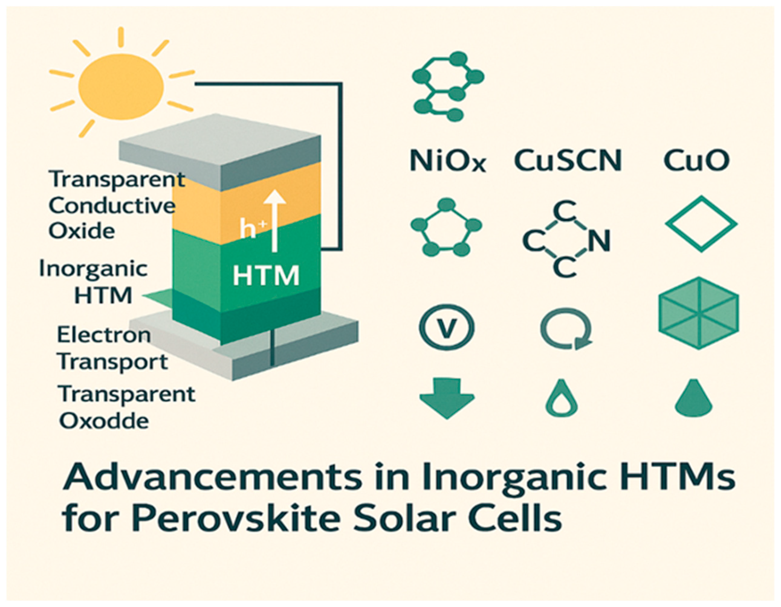
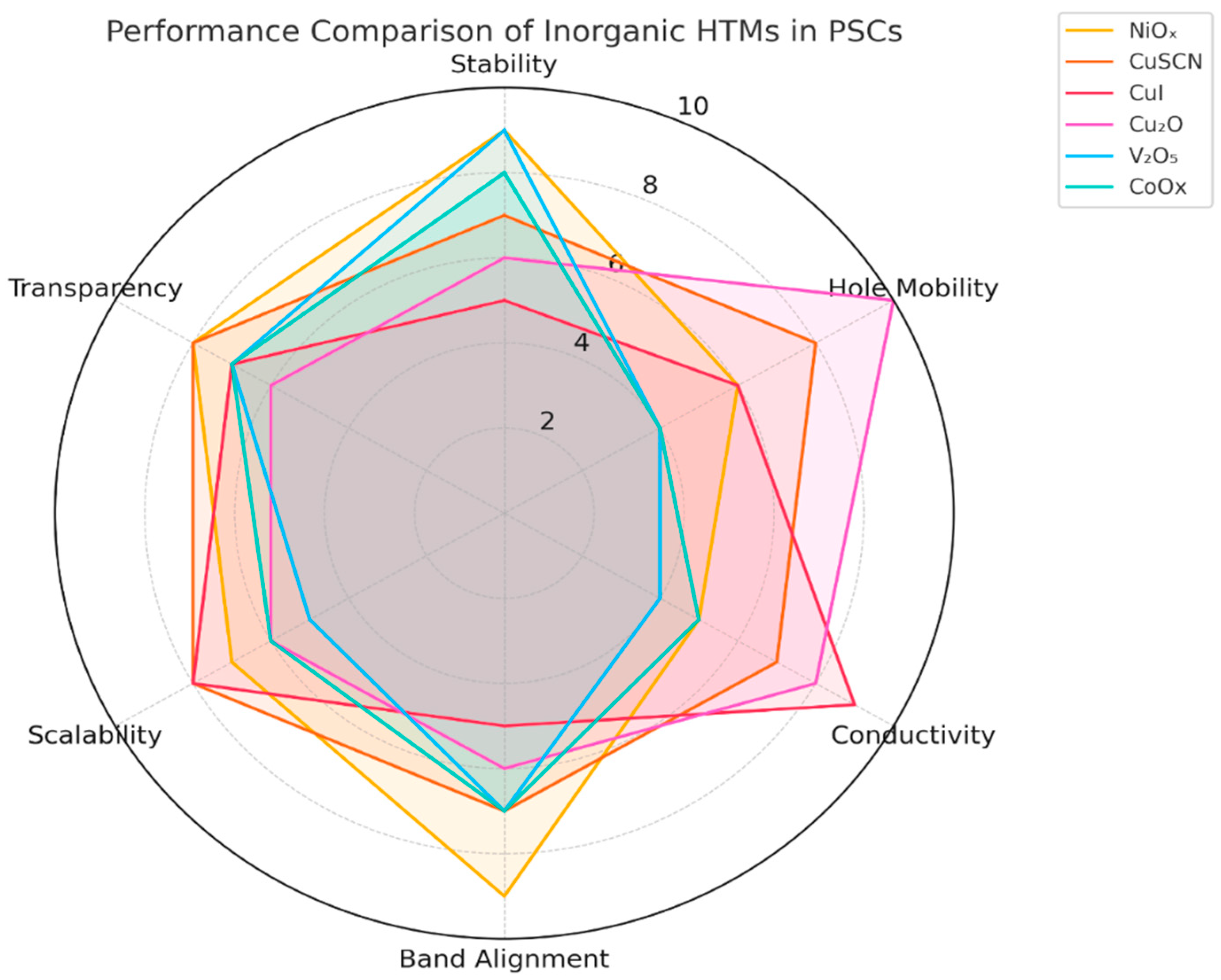
Energies 18 02374 g001
Figure 2. Rader plot of performance attributes in representative inorganic HTMs of perovskite solar devices: NiOx, CuSCN, CuI, Cu2O, V2O5, and CoOx. Literature-reported data for each parameter (stability, hole mobility, conductivity, band alignment, scalability, and transparency) are normalized to a 1–10 scale. This comparative visualization identifies trade-offs among alternative inorganic HTMs and aids in material selection for diverse PSC architectures.
Energies 18 02374 g002
Table 1. A quantitative comparison of inorganic HTMs in Table 1 shows their strengths and weaknesses in various key properties.
HTMBandgap (eV)Hole Mobility (cm2/V·s)Work Function (eV)Suitable for PSC TypeStabilityNotable Feature
NiOx+/−3.610−3–10−1~5.0Inverted (p–i–n)HighWidely used; ALD/sputtered films offer high stability [14,23,36]
CuSCN+/−3.6~10−2~5.3Normal (n–i–p)ModerateGood mobility and transparency; sensitive to humidity [34,38]
CuI~3.0–3.1~10−3~5.1Normal (n–i–p)Low–Mod.Easy processing but suffers from recombination and instability [35]
Cu2O~2.1Up to 256~5.0Normal (n–i–p)ModerateHigh hole mobility; lower absorption in the visible range [39]
V2O5~2.3–2.8~10~5.3Inverted (p–i–n)HighWide bandgap; low conductivity; often used with dopants [40]
CoOx~2.4–2.8~10~5.2Inverted (p–i–n)HighEmerging material; promising electrochemical performance [41]
Table 2. Physical, electrical, and thermal properties of prominent inorganic HTMs.
MaterialBandgap (eV)Hole Mobility (cm2/V·s)Work Function (eV)Conductivity (S/cm)ProcessabilityThermal StabilityReferences
NiOx3.6–4.010−3–10−1~5.010⁴–10−2ALD; Sputtering; Sol–GelExcellent[13,14,23]
CuSCN~3.6~10−2~5.310−2–10−3Spin-coating; ElectrodepositionGood[34,38]
CuI~3.1~10−3~5.1~1Spin-coating; Drop-castingModerate[35]
Cu2O2.0–2.2Up to 256~5.010⁴–10−2ALD; Oxidation; SputteringModerate[27,39]
V2O52.3–2.8~10~5.3LowThermal evaporation; Sol–GelHigh[40]
CoOx2.4–2.8~10~5.2ModerateSputtering; Sol–GelHigh[41]
Table 3. Suitability of HTMs in device architectures.
HTMCompatible ArchitectureTypical Deposition MethodPeak PCE Reported (%)NotesReferences
NiOxInverted (p–i–n)Sputtering; ALD; Sol–gel21.50%Most used inorganic HTM[14,23,27]
CuSCNNormal (n–i–p)Solution; Electrodeposition16.60%Transparent and cost-effective[34,38]
CuINormal (n–i–p)Spin-coating; Drop-casting~6–12%Prone to recombination[35]
Cu2ONormal (n–i–p)ALD; Oxidation13.30%High mobility and poor long-wavelength absorption[27,39]
V2O5Inverted (p–i–n)Evaporation; Sol–Gel~19%Good chemical barrier[40]
CoOxInverted (p–i–n)Sputtering; Sol–Gel~18%Still under active study[41]
Table 4. Deposition techniques for HTMs.
TechniqueTypeCostScalabilitySuitable HTMsKey NotesReferences
Spin-coatingSolution-basedLowModerateCuI, CuSCNLab-scale standard[34,35]
ElectrodepositionSolution-basedLowHighCuSCN, Cu2OLow-temperature and scalable[38,39]
Atomic Layer Deposition (ALD)Vapor-phaseHighHighNiOx, Cu2OUniform films; precise control[14,23]
SputteringPhysical vaporMediumHighNiOx, CoOx, Cu2OHigh reproducibility[27,41]
Slot-Die CoatingSolution-basedLowVery HighNiOx (sol–gel)Roll-to-roll compatible[23]
Blade CoatingSolution-basedLowVery HighNiOx, CuSCNSimple; scalable[38]
Disclaimer/Publisher’s Note: The statements, opinions and data contained in all publications are solely those of the individual author(s) and contributor(s) and not of MDPI and/or the editor(s). MDPI and/or the editor(s) disclaim responsibility for any injury to people or property resulting from any ideas, methods, instructions or products referred to in the content.

