Article

Optimization of the Boron Back Surface Field Produced with Reduced Thermal Steps in Bifacial PERT Solar Cell

by
Thais Crestani
,
Izete Zanesco
*,
Adriano Moehlecke
,
Lucas Teixeira Caçapietra Pires da Silva
and
João Victor Zanatta Britto
Solar Energy Technology Nucleus (NT-Solar), School of Technology, Pontifical Catholic University of Rio Grande do Sul (PUCRS), Porto Alegre 90619-900, RS, Brazil
*
Author to whom correspondence should be addressed.
Energies 2025, 18(9), 2347; https://doi.org/10.3390/en18092347
Submission received: 17 March 2025 / Revised: 23 April 2025 / Accepted: 30 April 2025 / Published: 3 May 2025

Abstract

:
Bifacial solar cells are the leading technology, and the number of steps in the manufacturing process influences the processing time and production cost. The goal of this paper is to optimize the boron back surface field (B-BSF) produced with reduced thermal steps and to analyze its influence on the electrical parameters and bifaciality coefficients of p-type bifacial PERT solar cells. The boron diffusion and a silicon oxide layer grown as a phosphorus diffusion barrier were carried out in a single thermal step, according to the patent granted BR102012030606-9. The sheet resistance of the emitter and B-BSF were not affected by the reduced thermal steps, demonstrating the effectiveness of the silicon oxide layer as a barrier to phosphorus diffusion in the boron-doped side. The short-circuit current density with incident irradiance on the boron-doped side was impacted by the B-BSF sheet resistance, affecting the efficiency and the maximum power bifaciality coefficient. The high recombination in the pp+ region limited the maximum power bifaciality coefficient to approximately 0.7, which is typical in p-type solar cells. Considering the achieved results, the boron and phosphorus diffusion performed with reduced thermal steps produces bifacial p-PERT solar cells with typical bifaciality, avoiding two thermal steps for silicon oxide growth and chemical etching and cleaning.

1. Introduction

The aluminum back surface field (Al-BSF) solar cell is gradually being replaced by the passivated emitter and rear solar cell (PERC) and tunnel oxide passivated contact solar cells (TOPCon). In the last decade, the dominant approach has been PERC technology, which is manufactured with p-type monocrystalline silicon wafers and passivation layers of AlOx [1,2,3] and SiNx [4,5,6], as shown in the configuration presented in Figure 1a. TOPCon solar cells manufactured with n-type monocrystalline silicon have the structure illustrated in Figure 1b. Forecasts indicate that this solar cell will gain market share in the next decade. Both solar cell structures enabled the industrial manufacturing of bifacial solar cells, which have a market share of approximately 85–90% [7].
A feature of the PERC configuration is the reduction in minority charge carrier recombination at the rear side due to the reduction in the metal/semiconductor contact area and the formation of a passivation layer. The rear passivation also increases internal reflectance, which contributes to enhanced energy conversion efficiency. The first high-efficiency PERC solar cell was reported in 1988, with an efficiency of 21.8%, as a result of a research project at the University of New South Wales. This technology has evolved, and AlOx has been found to be an effective material for passivation of the boron back surface field (B-BSF) and for producing field effect mechanisms [8].
The passivated emitter and rear totally diffused (PERT) solar cell is a device of the PERC family. To manufacture p-type bifacial PERT solar cells, which have the structure depicted in Figure 2, both phosphorus diffusion and boron diffusion are performed to form the emitter and the back surface field (BSF), respectively. Reducing the number of steps in the solar cell manufacturing process is crucial to the competitiveness of solar cell technologies. The number of steps in the manufacturing process influences the processing time and production cost. In addition, a reduction in the number of thermal steps has an impact on device quality, increasing minority carrier lifetime and decreasing process costs, such as those associated with gases and energy [8,9,10,11].
The manufacturing process of n-type PERT solar cells based on a single thermal process to form boron-doped and phosphorus-doped regions [12] was investigated with two simplifications of the thermal process. The first method involved co-diffusion of boron and phosphorus, with a gaseous phosphorus source and a boron-doped dielectric layer produced by low-frequency plasma-enhanced chemical vapor deposition (PECVD). The second process consisted of independent ion implantation of phosphorus and boron, followed by an annealing/activation step. In both cases, the open-circuit voltage (VOC) of 660–670 mV was similar to that obtained with the standard process. PERT solar cells produced with these processes in Czochralski silicon (Si-Cz) wafers achieved a conversion efficiency of 19.7% [12]. In n-PERT bifacial solar cells, rear-side passivated contacts can improve efficiency. Considering this fact, Ingenito et al. [13] reported a certified conversion efficiency of 22.8% with incident irradiance on the emitter of bifacial n-PERT solar cells. These devices were produced with a homogeneous boron emitter and phosphorus-doped polysilicon deposited by DC sputtering on thin silicon oxide.
The investigation of boron concentration as a function of depth (doping profile) produced by boron diffusion with BBr3 confirmed that better passivation was achieved in n-PERT solar cells with low surface concentration. Consequently, solar cells with higher efficiency have emitter profiles with low surface concentration and high junction depth [14]. With this solar cell configuration, Bektas et al. [15] investigated the influence of the boron doping profile produced with BBr3 on the quality of the p+ emitter and the contact resistance at the interface of the emitter and Ag/Al paste. The reduction in the boron concentration led to a decrease in carrier recombination in the noncontacted region, which diminished the saturation current. Nevertheless, a decrease in the boron concentration increased the contact resistance and recombination in the contacted areas of the emitter [15].
An alternative method to produce boron diffusion is to deposit the dopant on one face of the silicon wafer via the spin coating technique, which may reduce the number of processing steps. The boron doping profile produced by spin coating deposition presented a low surface concentration after wet oxidation [16]. Additionally, boron diffusion by the spin coating deposition to form the emitter in n-type silicon wafers resulted in a high bulk minority carrier lifetime and solar cell efficiency of 19.38%, which was similar to that obtained by boron diffusion with BBr3 [16]. With a reduction in the number of thermal steps, p-type solar cells were processed with a passivation layer of silicon oxide and spin coating deposition to form the B-BSF. An efficiency of 17.3% was obtained [17].
The doping profile of phosphorus emitters formed with POCl3 as the dopant source was investigated by Tang et al. [18]. The surface doping concentration was reduced from 6.6 × 1021 cm−3 to 3.9 × 1021 cm−3 after annealing at 700 °C, and the doping profile remained almost constant below a depth of 20 nm. The sheet resistance increased from 66 Ω/sq to 75 Ω/sq, and the uniformity of the sheet resistance was improved with an annealing step. The solar cells manufactured via mass production with an annealing step had an average conversion efficiency of 18.63%, which was 0.35% and 0.20% higher than that of devices manufactured with an emitter of ~66 Ω/sq and ~75 Ω/sq without annealing, respectively [18].
Bifacial PERC solar cells were developed with gallium-doped p-type monocrystalline silicon wafers and a SiNx/SiOxNy/SiNx stack layer for rear passivation. Efficiencies of 22.91% and 17.25% were achieved with incident solar irradiance on the phosphorus selective emitter and on the rear face, respectively. Solar cells with a stack layer presented a conversion efficiency with incident irradiance on the rear side 1.55% (absolute) greater than that of solar cells passivated with a single SiNx film. With a stack layer, the bifaciality coefficient of maximum power increased from 0.685 to 0.753 [19].
The investigation of passivation with SiO2/AlOx/SiNx stack layers revealed effective passivation of both p+ and n+ heavily doped regions due to the complementary effects of chemical passivation and field effect mechanisms [20]. The passivation configuration resulted in bifacial p-PERT solar cells industrially manufactured via ion-implanted technology with efficiencies of 20.5% (incident irradiance on the emitter) and 19.8% (incident irradiance on the rear face). These results were achieved in rear-textured solar cells, leading to a maximum power bifaciality coefficient of 0.98 [20].
In bifacial solar cells, surface passivation is crucial for reducing minority charge carrier recombination and for achieving a high bifaciality coefficient. Investigations have shown that passivation is usually more effective in the n+ emitter than in the p+ region doped with boron and that passivation with silicon oxide layers can be effective for p+ heavily doped regions [21]. The reduction in the surface recombination velocity provided by the SiO2 passivation layers impacted the history of the silicon solar cell. This dielectric allowed the development of the first advanced solar cell architectures, such as interdigitated back contact (IBC) and PERC solar cells, with efficiencies above 20% [21].
The growth of a selective epitaxial layer to reduce minority charge carrier recombination in solar cells with bifacial SiO2/AlOx/SiNx passivation on both p+ and n+ regions was investigated. A selective epitaxial growth process at 700 °C was developed, which was compatible with emitter passivation by SiO2 layers, thermal growth, or PECVD. A 500 nm p-type epitaxial layer was grown locally on the emitter contacts in a single step, with dielectric patterning via laser ablation and metallization by electroplating. Compared with the reference solar cells without an epitaxial layer, the average VOC of the bifacial devices with a p-type epitaxial layer was +6 mV, and the fill factor (FF) was +1% (absolute). With this configuration, a solar cell efficiency of 22.1% was achieved with incident irradiance on the emitter [22].
Considering the advantages of reducing thermal steps and the above discussion about sheet resistance of boron-doped regions, the goal of this paper is to optimize the sheet resistance of B-BSF, which is produced with a reduction in thermal steps, and to analyze its influence on the electrical parameters and bifaciality coefficient of p-type PERT bifacial solar cells. The main scientific contribution of this article is the development of bifacial p-PERT solar cells with sheet resistance of B-BSF experimentally optimized and produced in the same thermal step of silicon oxide growth as a phosphorus diffusion barrier, according to the patent granted BR102012030606-9 [11]. Compared to the standard diffusion of phosphorus (POCl3) and boron (BBr3), the optimized process avoids two thermal steps to grow silicon oxide layers as diffusion barriers and chemical etching and cleaning. The first suppressed thermal step is usually performed to grow a silicon oxide layer for producing the boron diffusion in only one face of the silicon wafer. The second avoided step is required to grow a silicon oxide layer on the boron-doped side to hinder the phosphorus diffusion in this face. The sheet resistance and profile of the dopant concentration as a function of depth were evaluated to demonstrate the effectiveness of the silicon oxide layer as a barrier to phosphorus diffusion on the boron-doped face, which was grown in the same thermal step of the boron diffusion. The performance of the bifacial solar cells was analyzed as a function of the sheet resistance of the B-BSF by means of the electrical parameters, bifaciality coefficients, and internal quantum efficiency.

2. Materials and Methods

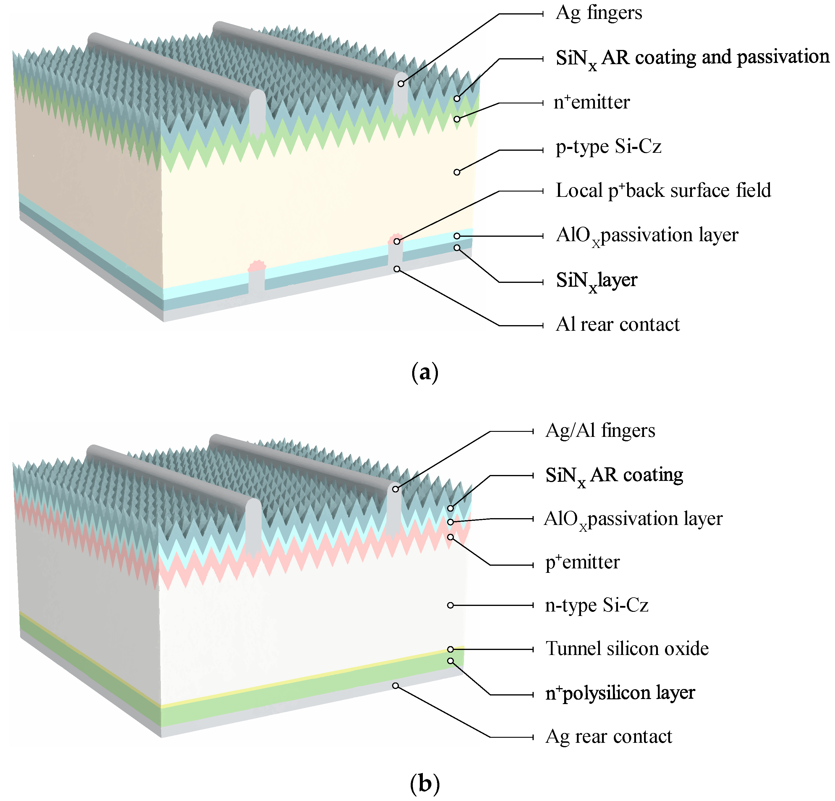
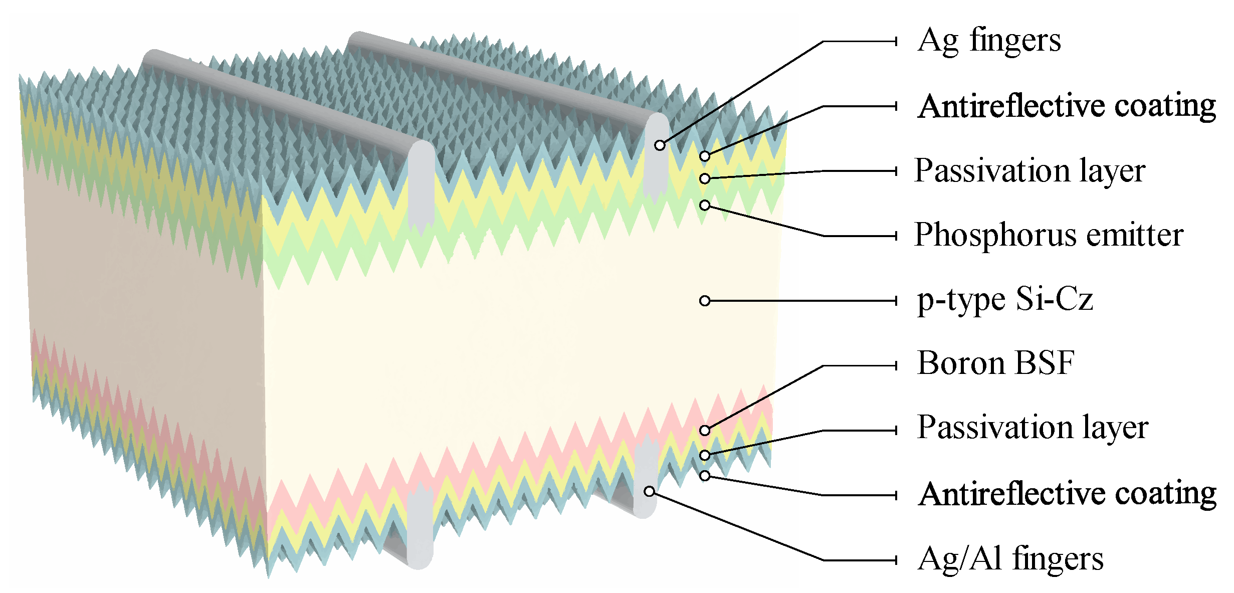
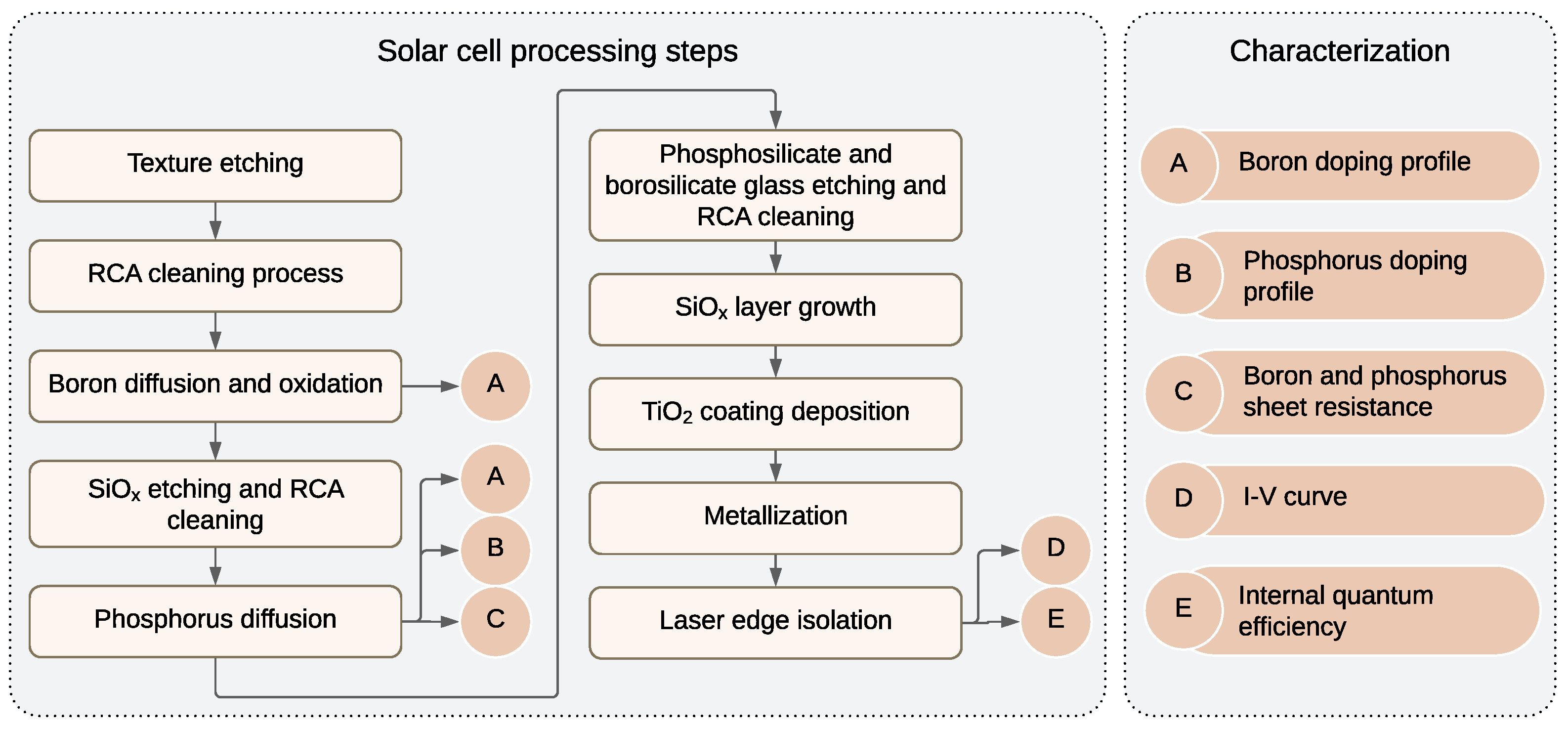
2.1. Solar Cell Production

Figure 3 shows the process sequence for manufacturing solar cells and the characterization methods adopted. Solar cells were processed in p-type Si-Cz wafers with a thickness of 200 μm, resistivity of 1 Ω.cm to 20 Ω.cm and average minority charge carrier lifetime ranging from 20 to 50 μs [23]. The structure of the n+pp+ bifacial PERT solar cells developed with a reduction in the number of thermal steps and silicon oxide passivation layers is presented in Figure 2.
Solar cell manufacturing started with an alkaline texture etching in a KOH solution. Before the thermal steps, the wafers were cleaned in RCA solution [24]. B-BSF was produced with a boron-containing liquid (PBF20, Filmtronics) via the spin coating technique to form a uniform thin layer on a surface of the silicon wafer.
After the evaporation of solvents, boron diffusion was performed in a quartz tube furnace at different temperatures from 950 °C to 980 °C, which resulted in B-BSF sheet resistance ranging from 30 to 53 Ω/sq. Considering as reference the standard boron and phosphorus diffusion in a silicon wafer to manufacture solar cells, the number of thermal steps to produce the B-BSF and phosphorus emitter were reduced, according to the process described in patent granted BR102012030606-9 [11]. In this approach, boron diffusion and silicon oxide growth as a barrier to phosphorus diffusion were carried out in a single thermal step, avoiding two high-temperature processes and reducing chemical cleaning and etching. In each batch, silicon wafers were introduced in the quartz tube at 700 °C, and the temperature was increased to 950, 960, 970, or 980 °C for the boron diffusion, which was performed with the oxygen and nitrogen concentration ratio of 1:4.5. The silicon oxide was grown on the borosilicate glass in two steps with oxygen flow in the quartz tube. In the first stage, the temperature decreased for 10 min at 900 °C, and in the second step, the temperature remained at 900 °C for 20 min. In the next step, nitrogen flow was introduced in the quartz tube, and the temperature decreased to 700 °C to extract the silicon wafers.
To produce the n+ emitter, the silicon oxide was etched in the wafer side without boron diffusion, and phosphorus was diffused at 845 °C in a quartz tube using POCl3 as the dopant source [25]. After boron and phosphorus diffusion, borosilicate and phosphosilicate glasses were removed. A thermal oxidation process at 800 °C was performed to passivate both surfaces with a silicon oxide layer [21]. The literature reported that a silicon oxide passivation layer thermally grown on the p+ emitter resulted in a higher minority charge carrier lifetime than that obtained with an AlOx/SiNx stack [26]. A TiO2 antireflective coating was deposited on both surfaces via electron beam evaporation. The thicknesses of the TiO2 thin films in the emitter and B-BSF regions were 50 nm and 90 nm, respectively [27]. Metallization was performed via screen printing of Ag/Al (p+ B-BSF) and Ag pastes (n+ emitter), which were fired at 860 °C. As the last step of the manufacturing process, before the characterization of the bifacial solar cells, the edge was isolated with a laser beam, resulting in devices with an area of 61.58 cm2.

2.2. Characterization of Solar Cells

The characterization of the samples and solar cells was performed as shown in Figure 3. The sheet resistance after boron (BSF) and phosphorus (emitter) diffusion was measured in 13 regions of a silicon wafer in each batch after the diffusion of both dopants. The average and standard deviation of the B-BSF (Rsh-B) and phosphorus emitter (Rsh-P) sheet resistances were calculated. To analyze the reproducibility of the boron diffusion performed in the same thermal step to grow silicon oxide on the borosilicate glass layer as a phosphorus diffusion barrier, three independent batches with a boron diffusion temperature (TB) of 950 °C and eight batches with a TB of 970 °C were processed. The Rsh-B was also formed at boron diffusion temperatures from 950 °C to 980 °C with a reduction in thermal steps, and after producing BSF and emitter, the boron and phosphorus sheet resistances were measured.
Profiles of boron and phosphorus concentrations as a function of depth were obtained in the same Si wafer in which the sheet resistance was measured via the ECV (electrochemical capacitance-voltage) method. The ECV is a destructive method, which consists of etching the surface of the sample with a solution of ammonium bifluoride. The silicon wafer is held on a support with two metal contacts, and a structure with a sealing ring creates an area in which the electrolyte forms an interface with the silicon wafer. The capacitance as a function of the applied voltage is measured for obtaining the concentration of dopant as a function of the depth. The accuracy of the ECV method is approximately ±10% [28]. The boron profiles obtained with the diffusion process at temperatures of 950 °C and 970 °C before and after phosphorus diffusion were compared.
The electric current as a function of voltage (I–V curve) of the bifacial solar cells with incident irradiance on the emitter and on the B-BSF was independently measured under standard conditions (1000 W/m2, AM1.5G, and 25 °C) in a class AAA solar simulator. The I–V curve of each solar cell was measured with incident irradiance on one face while the other face was kept in the dark.
The influence of Rsh-B on the short-circuit current density (JSC), open-circuit voltage (VOC), fill factor (FF), and efficiency (η) was investigated. To compare the electrical parameters, the relative values are presented. The internal quantum efficiency (IQE) with incident irradiance on the emitter and on the B-BSF of the solar cell with the highest efficiency was compared.
The bifaciality coefficients, defined in the IEC 60904-24 standard, are presented and discussed as a function of Rsh-B. Equation (1) represents the bifaciality coefficient of the output power at the point of maximum power (δPMP), which is the ratio of the maximum power output (PMP) with incident irradiance on the face with the lowest efficiency to the maximum power obtained with illumination on the side with the highest efficiency. Similarly, with (2) and (3), the bifaciality coefficients of the short-circuit current and open-circuit voltage can be calculated.
δ P M P = η B S F η e m i t t e r
δ I S C = I S C B S F I S C e m i t t e r
δ V O C = V O C B S F V O C e m i t t e r

3. Results and Discussion

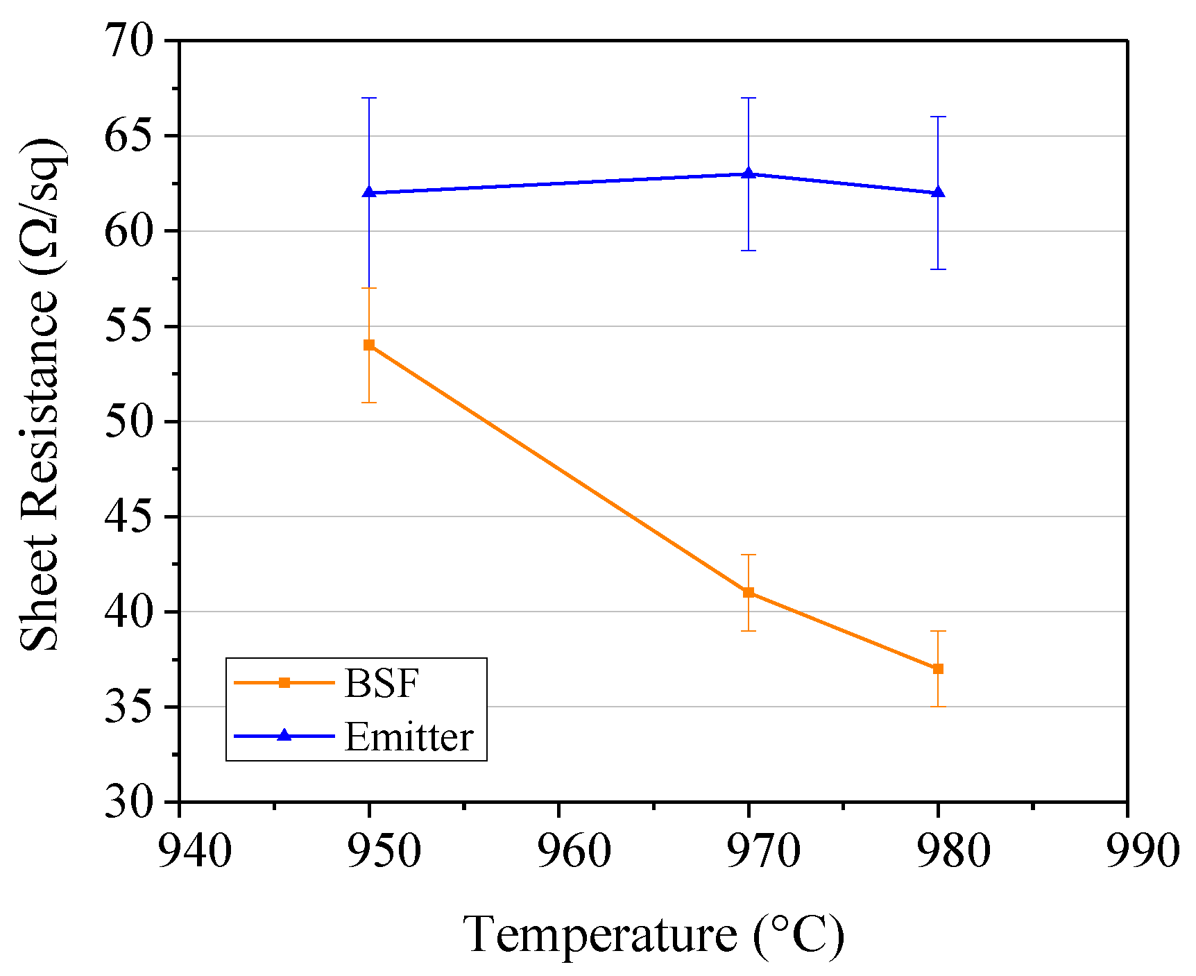
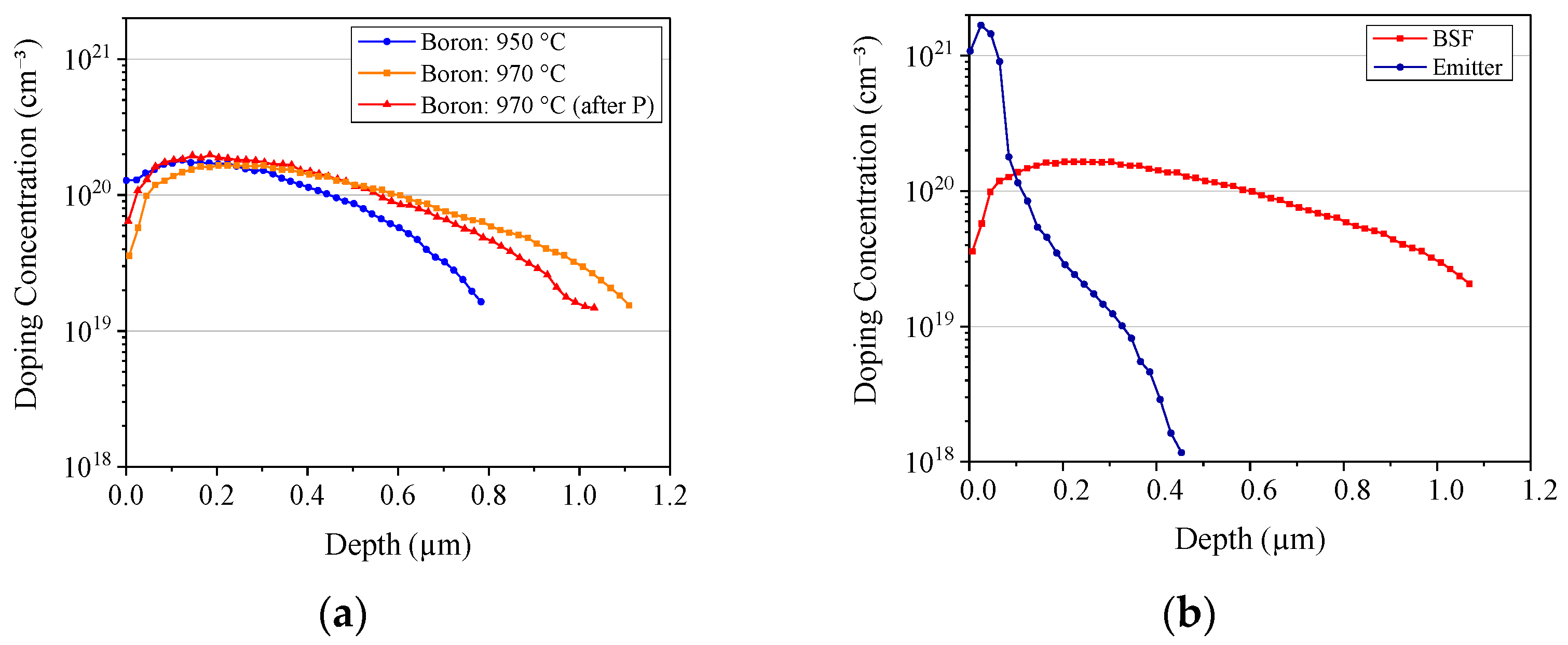
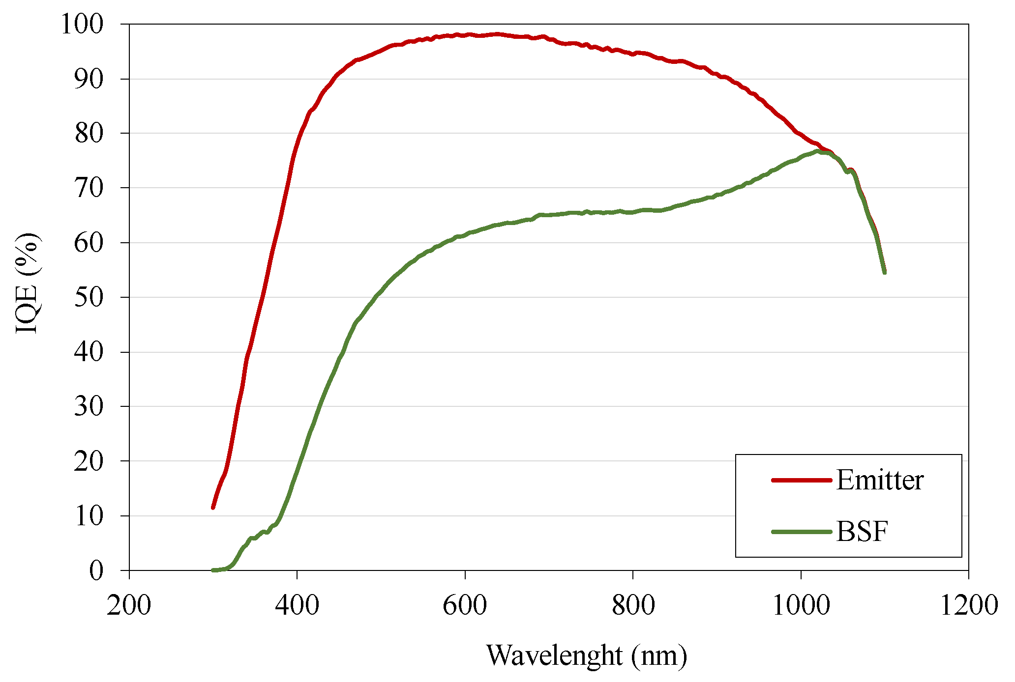
3.1. Characterization of the Back Surface Field and Emitter

Table 1 shows the average sheet resistance of B-BSF (Rsh-B) produced at temperatures of 950 °C (BTB950) and 970 °C (BTB970) in different batches. To evaluate the effectiveness of boron diffusion and the growth of a borosilicate glass layer performed at the same thermal step as a barrier to phosphorus diffusion, the average sheet resistance of the phosphorus emitter (Rsh-P) is presented.
The average sheet resistances of the B-BSF obtained at temperatures of 950 °C and 970 °C were (54 ± 3) Ω/sq and (41 ± 2) Ω/sq, respectively. The low standard deviation of 5–6% demonstrates that the boron diffusion process with a reduction in the number of thermal steps is repeatable. The value of the standard deviation obtained for the average sheet resistance is typical for boron diffusion in monocrystalline silicon wafers, regardless of the diffusion method. A nonuniformity of 5.3% was reported for a p+ emitter produced using BCl3 in a low-pressure quartz tube at 1050 °C [29]. With spin coating deposition to produce the p+ emitter, a homogeneous sheet resistance of (73 ± 5) Ω/sq was reported in the literature, which is similar to the sheet resistance of (78 ± 7) Ω/sq obtained using BBr3 [16].
The average sheet resistances of the B-BSF and phosphorus emitter as a function of boron diffusion temperature are shown in Figure 4. As expected, the B-BSF sheet resistance decreased with increasing boron diffusion temperature. The Rsh-P was not affected by the boron diffusion temperature in the range from 950 °C to 980 °C. The average Rsh-P was similar and ranged from (62 ± 5) Ω/sq (TB = 950 °C) to (63 ± 4) Ω/sq (TB = 970 °C), demonstrating the effectiveness of the phosphorus and boron diffusion processes with a reduced number of thermal steps and showing the potential of the method to produce p-type bifacial PERT solar cells.
Figure 5 shows the dopant concentration as a function of depth in the silicon wafer, and Table 2 summarizes the junction depth and surface concentration of phosphorus and boron profiles for boron diffusion temperatures (TB) of 950 °C and 970 °C.
Figure 5a indicates that the surface concentration of boron (Cs-BSF) tended to decrease with an increase in TB from 950 °C to 970 °C, and as expected, the depth of B-BSF (xjBSF) increased. For TB = 970 °C, phosphorus diffusion slightly affected the boron profile, as shown in Figure 5a. After the diffusion of boron and phosphorus, the boron surface concentration was 6.4 × 1019 cm−3, with a slight increase in the surface concentration and up to the depth of 0.3 µm. This behavior is explained by the silicon oxide layer grown in the boron-doped face of the silicon wafer as a barrier to phosphorus diffusion being rich in boron, and this dopant continued to diffuse in the silicon during phosphorus diffusion. Moreover, in phosphorus diffusion, oxygen is introduced into the quartz tube, and the oxidation process remains, increasing the barrier silicon oxide thickness on the boron-doped side. Both processes at high temperature caused a reduction in boron depletion in the surface of the BSF, which improved the performance of the bifacial solar cell [29]. The produced boron profile with reduction in the number of thermal steps was similar to those reported in the literature, where the boron surface concentration was on the order of 1019 cm−3 in the Si-Cz substrate [14,18,30]. Li et al. [30] reported values of 2.8 × 1019 cm−3 for a boron emitter in n-PERT solar cells. Therefore, the silicon oxide layer grown on the boron-doped face in the same thermal step of the boron diffusion was effective as a barrier to phosphorus diffusion.
Figure 5b shows that the surface concentration of the phosphorus emitter (CSemitter) was higher than that of the B-BSF. As presented in Table 2, the values of the CSemitter and the emitter junction depth (xjemitter) were approximately 1.1 × 1021 cm−3 and 0.5 μm, respectively. The produced phosphorus doping profile is typical for PERC solar cells [14].

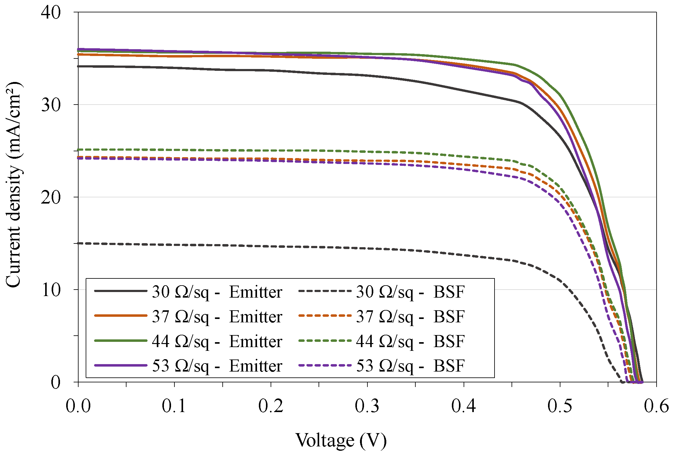
3.2. Influence of the B-BSF Sheet Resistance on Electrical Characteristics

The J–V curves of the bifacial solar cells developed with a reduction in the number of thermal steps are shown in Figure 6. The electrical characteristics were measured with incident irradiance independently on each face under standard test conditions. Figure 6 indicates that the JSC obtained with illumination of the BSF is the electrical parameter mainly affected by the B-BSF sheet resistance.
In Figure 7 and Table 3, the influence of the B-BSF sheet resistance on the relative electrical parameters of the developed bifacial PERT solar cells with incident irradiance on the emitter and on the BSF is compared.
Figure 7a confirms that the relative JSC measured with irradiance on the B-BSF is the electrical parameter most affected by the sheet resistance. Moreover, this electrical parameter obtained with incident irradiance on the BSF is lower than that measured with illumination on the emitter, which affects the relative efficiency, as shown in Figure 7d. Table 3 shows that the relative JSC was slightly affected by Rsh-B when the bifacial solar cells were characterized by illumination of the emitter, ranging from 0.97 to 1.0. However, when the developed solar cells were characterized with illumination of the B-BSF, the influence of Rsh-B was high on the relative JSC, which varied from 0.42 to 0.75. Consequently, the relative efficiency with incident irradiance on the p+ BSF ranged from 0.40 to 0.72 for a sheet resistance from 30 to 53 Ω/sq, in contrast to the variation of 0.90–1.0 with irradiance on the emitter. The reduction in JSC with irradiance on the B-BSF is due to the high minority carrier recombination, which is typical of the pp+ region, as reported in the literature [10,31].
Figure 7b,c shows that the VOC and FF with incident irradiance on the BSF are similar to the values obtained with illumination on the emitter and that these parameters are slightly affected by the B-BSF sheet resistance. Table 3 confirms the low impact of Rsh-B on the relative FF, which showed a slight decrease for the high Rsh-B because the contact resistance between the boron-doped BSF and the metal fingers increased. The relative fill factor ranged from 0.95 to 1.0 and from 0.96 to 0.99 with incident irradiance on the phosphorus emitter and on B-BSF, respectively. The relative VOC obtained with incident irradiance on the emitter and B-BSF are similar, as shown in Figure 7b and Table 3. The range of the relative VOC was 0.99 to 1.0 with illumination of the emitter and 0.97–0.98 with irradiance on the p+ region, indicating that the minority charge carrier lifetime in the bulk is suitable for producing bifacial solar cells.
The analysis of Figure 7d indicates that the sheet resistance of B-BSF of approximately 44 Ω/sq led to higher efficiency with incident irradiance on the emitter. With illumination of the BSF, the efficiency increased up to Rsh-B of 37 Ω/sq, remaining close to this value for higher sheet resistance. The efficiency with incident irradiance on the emitter of the bifacial p-type solar cells was 17.0%. This result approaches the efficiency of 19.38%, reported for n-type solar cells produced with the method of spin coating deposition of boron solution [16]. With simplifications of the thermal process, Blévin et al. reported the efficiency of 19.7% in n-PERT solar cells [12].

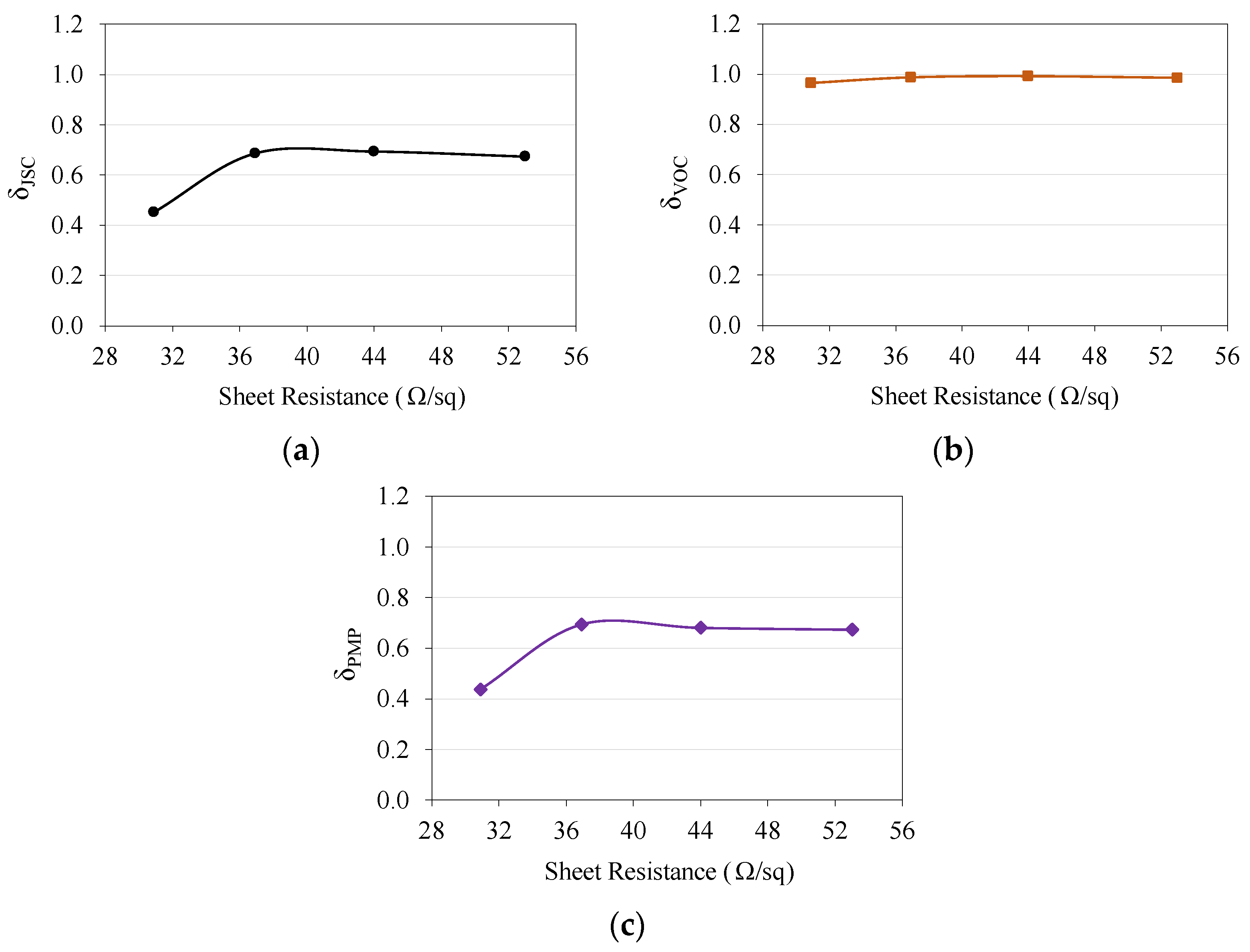
3.3. Influence of BSF Sheet Resistance on Bifaciality Coefficients

Figure 8 shows the bifaciality coefficients of the JSC, VOC, and PMP of the bifacial PERT solar cells developed with a reduction in the number of thermal steps. The sheet resistance of the B-BSF affected mainly the bifaciality coefficient of the short-circuit current density, which impacted the bifaciality coefficient of the maximum power output. Consequently, the bifaciality coefficients depicted in Figure 8a,c showed similar trends with an increasing B-BSF sheet resistance. The bifaciality coefficient of the open-circuit voltage was slightly affected by Rsh-B.
The bifaciality coefficient of JSC decreased for a sheet resistance lower than 37 Ω/sq because of higher carrier recombination in the pp+ region. Therefore, charge carrier recombination in the boron BSF is the limiting factor of the bifaciality coefficient of the short-circuit current density in p-type bifacial PERT solar cells. The maximum power bifaciality coefficient obtained with a sheet resistance higher than 37 Ω/sq is approximately 0.7, which is similar to the JSC bifaciality coefficient reported in the literature for p-type solar cells [7,10].
The internal quantum efficiency (IQE) of the solar cell with higher efficiency and incident irradiance on the B-BSF and emitter is compared in Figure 9. The IQE with incident irradiance on the emitter was low for wavelengths lower than 400 nm because of the recombination of charge carriers in the emitter with an Rsh-P of approximately 60 Ω/sq.
However, the IQE with illumination on the B-BSF was lower than that obtained for the emitter at wavelengths lower than 500 nm because of the higher recombination of minority charge carriers in the pp+ region. This result is not related to the boron diffusion process with reduced thermal steps but rather to the feature of the pp+ region doped with boron [32]. Experimental investigations demonstrated higher recombination in the p+ emitter than in the n+ emitter [32]. Two reasons may explain this result. One reason is the higher minority charge carrier recombination capture cross section of minority charge carriers (electrons) in p+ boron-doped silicon than that of the holes in the n+ emitter. Another reason for the difference in recombination in n+ and p+ heavily doped silicon is the higher surface recombination velocity of minority charge carriers (electrons) in the p+ region. In this investigation, the passivation of a silicon dioxide layer, which was thermally grown, reduced the surface recombination, but it was less effective in the boron-doped silicon than in the phosphorus-doped silicon. To improve the performance of bifacial solar cells with illumination of the pp+ region, thinner boron BSF and other dopants, such as gallium, may be explored. With respect to these approaches, effective and innovative methods of passivating the p+ surface have focused on field effect mechanisms [19,33], and the development of a floating junction [34] should be investigated.
The minority carrier lifetime in the bulk also caused the low IQE with illumination of the B-BSF. However, with incident irradiance on the emitter, the low recombination of minority carriers in the phosphorus-doped region led to higher IQE values for wavelengths longer than 400 nm [31]. This result can be explained by the fact that with illumination of the emitter and the known absorptance of silicon, many charge carriers photogenerated near the p-n junction have a high probability of being collected. On the other hand, with incident irradiance on the B-BSF, the high recombination in the p+ region reduced the concentration of photogenerated charge carriers. Therefore, the minority carriers may recombine before being collected by the faraway pn junction. At wavelengths higher than 1000 nm, the IQE with incident irradiance on the emitter is similar to that found with illumination of the BSF, confirming the low minority carrier recombination in the emitter and the high recombination in the B-BSF.

4. Conclusions

The boron diffusion and the growth of a silicon oxide layer as a barrier to phosphorus diffusion in a single thermal step to form the B-BSF in bifacial PERT solar cells is reproducible. In p-type Si-Cz wafers with resistivity ranging from 1 Ω.cm to 20 Ω.cm, the standard deviation of the B-BSF sheet resistance produced in different batches at temperatures of 950 °C and 970 °C was 5–6%. Moreover, boron diffusion did not affect the sheet resistance of the phosphorus emitter, leading to a phosphorus sheet resistance of (62 ± 5) Ω/sq for TB = 950 °C and a similar value of (63 ± 4) Ω/sq for TB = 970 °C. Phosphorus diffusion slightly affected the boron concentration profile. At a boron diffusion temperature of 970 °C, the thermal step to diffuse phosphorus slightly increased the surface boron concentration from 3.6 × 1019 cm−3 to 6.4 × 1019 cm−3, demonstrating the effectiveness of the silicon oxide layer grown in the same thermal step of the boron diffusion as a barrier to phosphorus diffusion. These results indicate that the boron diffusion process with reduced thermal steps can be used to produce p-type bifacial PERT solar cells.
The boron sheet resistance mainly affected the relative short-circuit current density with incident irradiance on the boron-doped region, leading to a low bifaciality coefficient of this parameter. The minority charge carrier recombination in the BSF region reduced mainly the relative short-circuit current density with incident irradiance in the pp+ region. However, the relative open-circuit voltage and fill factor with incident solar irradiance on the B-BSF were similar to the values found with radiation reaching the emitter and were slightly affected by the BSF sheet resistance. A boron sheet resistance of 44 Ω/sq resulted in an efficiency of 17.0% with incident irradiance on the emitter of the bifacial solar cell.
A low bifaciality coefficient of the short-circuit current density was obtained for a low boron sheet resistance because of higher recombination in the pp+ region, which impacted the bifaciality coefficient of the maximum power output. For sheet resistance higher than 36 Ω/sq a typical value reported for p-type solar cells, of approximately 0.7, was found for the bifaciality coefficient of maximum power output. On the other hand, the bifaciality coefficient of the open-circuit voltage was slightly affected by the boron sheet resistance.
The internal quantum efficiency of solar cells with incident irradiance on the emitter is greater than that with irradiance reaching the B-BSF at wavelengths between 300 and 500 nm, indicating the effectiveness of silicon oxide passivation and the low recombination of minority carriers in the emitter region. High recombination in the pp+ region reduced the internal quantum efficiency with irradiance reaching this face, as reported in the literature.
In summary, bifacial p-PERT solar cells were developed with sheet resistance of B-BSF optimized and performed with a new dopant diffusion process with a reduced number of thermal steps. The boron diffusion and silicon oxide growth as a phosphorus diffusion barrier were performed in a single thermal step, according to the patent granted BR102012030606-9 [11], which avoided two high-temperature steps and chemical etching and cleaning. The sheet resistance and profile of dopant concentration demonstrated the effectiveness of the silicon oxide layer as a barrier to phosphorus diffusion in the boron-doped side. The limitation of the bifacial p-PERT solar cell is the high recombination in the pp+ region, which affected mainly the relative short-circuit current density with incident irradiance on the B-BSF and the bifaciality coefficient of maximum power output.
In future research, we suggest optimizing the B-BSF to produce bifacial PERT solar cells in different substrates, such as n-type Si-Cz and Si-FZ, and in silicon wafers with high resistivity, which may improve the bifacial coefficients. Additionally, methods to produce the pp+ region with low minority carrier recombination, exploring other p+ dopants, boron diffusion methods, and the formation of floating junctions may be investigated. For industrial applications, the dopant diffusion process with reduced thermal steps should be investigated in a pilot plant to manufacture bifacial PERT solar cells.

Author Contributions

Conceptualization, I.Z. and T.C.; methodology, I.Z., T.C. and A.M.; formal analysis, T.C., I.Z. and J.V.Z.B.; investigation, T.C., J.V.Z.B. and L.T.C.P.d.S.; data curation, J.V.Z.B. and L.T.C.P.d.S.; writing—original draft preparation, T.C.; writing—review and editing, I.Z. and A.M.; visualization, T.C. and J.V.Z.B.; supervision, I.Z.; project administration, I.Z. and A.M.; funding acquisition, I.Z. and A.M. All authors have read and agreed to the published version of the manuscript.

Funding

This research was funded by the Brazilian funding agency CNPq (National Council for Scientific and Technological Development), grant numbers 305554/2021-2 and 306916/2017-7, and the Brazilian electric utility “Eletrosul Centrais Elétricas S.A”, grant number 1110140010. The APC was funded by National Council for Scientific and Technological Development.

Data Availability Statement

Data contained within the article.

Acknowledgments

The authors acknowledge the financial support of the Brazilian funding agency CNPq (National Council for Scientific and Technological Development), grant numbers 305554/2021-2 and 306916/2017-7, and the Brazilian electric utility “Eletrosul Centrais Elétricas S.A”, grant number 1110140010. Thais Crestani is grateful for the grant provided by CAPES (Coordination for the Improvement of Higher Education Personnel).

Conflicts of Interest

The authors declare no conflicts of interest. The funders had no role in the design of the study; in the collection, analyses, or interpretation of data; in the writing of the manuscript; or in the decision to publish the results.

References

  1. Seguini, G.; Cianci, E.; Wiemer, C.; Saynova, D.; van Roosmalen, J.A.M.; Perego, M. Si Surface Passivation by Al2O3 Thin Films Deposited Using a Low Thermal Budget Atomic Layer Deposition Process. Appl. Phys. Lett. 2013, 102, 131603. [Google Scholar] [CrossRef]
  2. Kühnhold, S.; Saint-Cast, P.; Kafle, B.; Hofmann, M.; Colonna, F.; Zacharias, M. High-Temperature Degradation in Plasma-Enhanced Chemical Vapor Deposition Al2O3 Surface Passivation Layers on Crystalline Silicon. J. Appl. Phys. 2014, 116, 054507. [Google Scholar] [CrossRef]
  3. Cho, Y.J.; Shin, W.C.; Chang, H.S. Selective Deposition Contact Patterning Using Atomic Layer Deposition for the Fabrication of Crystalline Silicon Solar Cells. Thin Solid. Film. 2014, 568, 1–5. [Google Scholar] [CrossRef]
  4. Li, J.D.; Shen, G.S.; Chen, W.L.; Li, Z.; Hong, R.J. Preparation of SiNx Multilayer Films by Mid-Frequency Magnetron Sputtering for Crystalline Silicon Solar Cells. Mater. Sci. Semicond. Process 2017, 59, 40–44. [Google Scholar] [CrossRef]
  5. Li, H.; Wenham, S.R.; Shi, Z. High Efficiency PERL Cells on CZ P-Type Crystalline Silicon Using a Thermally Stable a-Si:H/SiNx Rear Surface Passivation Stack. Sol. Energy Mater. Sol. Cells 2013, 117, 41–47. [Google Scholar] [CrossRef]
  6. Lelièvre, J.-F.; Kafle, B.; Saint-Cast, P.; Brunet, P.; Magnan, R.; Hernandez, E.; Pouliquen, S.; Massines, F. Efficient Silicon Nitride SiNx:H Antireflective and Passivation Layers Deposited by Atmospheric Pressure PECVD for Silicon Solar Cells. Prog. Photovolt. Res. Appl. 2019, 27, 1007–1019. [Google Scholar] [CrossRef]
  7. VDMA. International Technology Roadmap for Photovoltaic (ITRPV); Frankfurt am Main; VDMA: Mumbai, India, 2024. [Google Scholar]
  8. Green, M.A. The Passivated Emitter and Rear Cell (PERC): From Conception to Mass Production. Sol. Energy Mater. Sol. Cells 2015, 143, 190–197. [Google Scholar] [CrossRef]
  9. Singha, B.; Solanki, C.S. Boron-Rich Layer Properties Formed by Boron Spin on Dopant Diffusion in n-Type Silicon. Mater. Sci. Semicond. Process 2017, 57, 83–89. [Google Scholar] [CrossRef]
  10. Crestani, T. Development of P-Type PERT Bifacial Solar Cells with Floating Junction and Passivation Analysis. Ph.D. Thesis, Pontifical Catholic University of Rio Grande do Sul, Porto Alegre, Brazil, 2021. [Google Scholar]
  11. Zanesco, I.; Moehlecke, A. Dopant Diffusion Process in Silicon Wafers to Manufacture Solar Cells. BR Patent nº BR 102012030606-9, 9 February 2021. [Google Scholar]
  12. Blévin, T.; Lanterne, A.; Grange, B.; Cabal, R.; Vilcot, J.P.; Veschetti, Y. Development of Industrial Processes for the Fabrication of High Efficiency N-Type PERT Cells. Sol. Energy Mater. Sol. Cells 2014, 131, 24–29. [Google Scholar] [CrossRef]
  13. Ingenito, A.; Allebé, C.; Libraro, S.; Ballif, C.; Paviet-Salomon, B.; Nicolay, S.; Diaz Leon, J.J. 22.8% Full-Area Bifacial n-PERT Solar Cells with Rear Side Sputtered Poly-Si(n) Passivating Contact. Sol. Energy Mater. Sol. Cells 2023, 249, 112043. [Google Scholar] [CrossRef]
  14. Mojrová, B.; Comparotto, C.; Kopecek, R.; Mihailetchi, V.D. Optimization of Boron Diffusion for Screen Printed N-PERT Solar Cells. Energy Procedia 2016, 92, 474–478. [Google Scholar] [CrossRef]
  15. Bektaş, G.; Aslan, S.; Keçeci, A.E.; Özyahni, V.; Canar, H.H.; Asav, H.; Seyrek, S.; Verlinden, P.J.; Turan, R. Influence of Boron Doping Profile on Emitter and Metal Contact Recombination for N-PERT Silicon Solar Cells. Sol. Energy Mater. Sol. Cells 2024, 272, 112886. [Google Scholar] [CrossRef]
  16. Barth, S.; Doll, O.; Koehler, I.; Neckermann, K.; Blech, M.; Lawerenz, A.; Edler, A.; Kopecek, R.; Schneider, J.J. 19.4 Efficient Bifacial Solar Cell with Spin-on Boron Diffusion. Energy Procedia 2013, 38, 410–415. [Google Scholar] [CrossRef]
  17. Moehlecke, A.; Zanesco, I. Development of Silicon Solar Cells and Photovoltaic Modules in Brazil: Analysis of a Pilot Production. Mater. Res. 2012, 15, 581–588. [Google Scholar] [CrossRef]
  18. Tang, L.; Li, W.; Tian, Y.; Xue, F.; Xin, Z.; Jiang, Q.; Pan, S. Post Annealing to Improve the Sheet Resistance and Uniformity of Emitter for Enhancing Conversion Efficiency of Mass-Produced Mc-Si Solar Cells. Mater. Sci. Semicond. Process 2022, 138, 106316. [Google Scholar] [CrossRef]
  19. Wei, P.; Tong, R.; Liu, X.; Wei, Y.; Zhang, Y.; Liu, X.; Dai, J.; Yin, H.; Liu, D. Optimization of Rear-Side Passivation for Enhancing the Performance of Bifacial PERC+ Solar Cells. Mater. Sci. Semicond. Process 2024, 170, 107947. [Google Scholar] [CrossRef]
  20. Huang, H.; Modanese, C.; Sun, S.; von Gastrow, G.; Wang, J.; Pasanen, T.P.; Li, S.; Wang, L.; Bao, Y.; Zhu, Z.; et al. Effective Passivation of P+ and N+ Emitters Using SiO2/Al2O3/SiNx Stacks: Surface Passivation Mechanisms and Application to Industrial p-PERT Bifacial Si Solar Cells. Sol. Energy Mater. Sol. Cells 2018, 186, 356–364. [Google Scholar] [CrossRef]
  21. Glunz, S.W.; Feldmann, F. SiO2 Surface Passivation Layers—A Key Technology for Silicon Solar Cells. Sol. Energy Mater. Sol. Cells 2018, 185, 260–269. [Google Scholar] [CrossRef]
  22. Recamán Payo, M.; Li, Y.; Russell, R.; Singh, S.; Kuzma Filipek, I.; Duerinckx, F.; Szlufcik, J.; Poortmans, J. Efficiency Gain in Plated Bifacial N-Type PERT Cells by Means of a Selective Emitter Approach Using Selective Epitaxy. Sol. Energy Mater. Sol. Cells 2020, 204, 110173. [Google Scholar] [CrossRef]
  23. Pinto, J.L. Optimization and Comparison of Processes to Form the Back Surface Field with Boron in Solar Cells. Ph.D. Thesis, Pontifical Catholic University of Rio Grande do Sul, Porto Alegre, Brazil, 2012. [Google Scholar]
  24. Kern, W. The Evolution of Silicon Wafer Cleaning Technology. J. Electrochem. Soc. 1990, 137, 1887. [Google Scholar] [CrossRef]
  25. Wehr, G.; Zanesco, I.; Moehlecke, A. Influence of Diffusion Parameters on Electrical Characteristics of Mc-Si Solar Cells with Aluminum and Phosphorus Diffusion Performed in the Same Thermal Step. Mater. Res. 2019, 22, e20180443. [Google Scholar] [CrossRef]
  26. Park, C.; Shim, G.; Balaji, N.; Park, J.; Yi, J. Correlation between Boron-Silicon Bonding Coordination, Oxygen Complexes and Electrical Properties for n-Type c-Si Solar Cell Applications. Energies 2020, 13, 3057. [Google Scholar] [CrossRef]
  27. Model, J.C.M.; Moehlecke, A.; Zanesco, I.; Ly, M.; Marcondes, T.L. TiO2 Antireflection Coating Deposited by Electro-Beam Evaporation: Thin Film Thickness Effect on Weighted Reflectance and Surface Passivation of Silicon Solar Cells. Mater. Res. 2022, 25, e20220245. [Google Scholar] [CrossRef]
  28. Bock, R.; Altermatt, P.P.; Schmidt, J. Accurate Extraction of Doping Profiles from Electrochemical Capacitance Voltage Measurements. In Proceedings of the 23rd European Photovoltaic Solar Energy Conference, Valencia, Spain, 1–5 September 2008; p. 1510. [Google Scholar]
  29. Peng, M.; Wang, Q.; Zhang, M.; Xi, X.; Liu, G.; Wang, L.; Chen, L. Optimization of Boron Depletion for Boron-Doped Emitter of n-type TOPCon Solar Cells. Mater. Sci. Semicond. Process 2024, 178, 108424. [Google Scholar] [CrossRef]
  30. Li, Y.; Shen, H.; Hou, Z.; Wei, Q.; Ni, Z.C.; Hu, D. Formation of Emitter by Boron Spin-on Doping from SiO2 Nanosphere and Properties of the Related n-PERT Solar Cells. Sol. Energy 2021, 225, 317–322. [Google Scholar] [CrossRef]
  31. Eisenberg, Y.; Kreinin, L.; Bordin, N.; Eisenberg, N. Effective Surface Recombination of p+ Layers Doped Using Ion Implantation or Surface Deposited B Sources. Energy Procedia 2016, 92, 16–23. [Google Scholar] [CrossRef]
  32. Siddiqui, A.; Bektaş, G.; Nasser, H.; Turan, R.; Usman, M. Impact of Ion Implantation and Annealing Parameters on Bifacial PERC and PERT Solar Cell Performance. Sustain. Energy Technol. Assess. 2022, 53, 102583. [Google Scholar] [CrossRef]
  33. Min, K.H.; Hwang, J.M.; Chen, C.; Choi, W.J.; Upadhyaya, V.D.; Bounsaville, B.; Rohatgi, A.; Ok, Y.W. Enhanced Passivation and Stability of Negative Charge Injected SiNx with Higher Nitrogen Content on the Boron Diffused Surface of N-Type Si Solar Cells. Sol. Energy Mater. Sol. Cells 2024, 273, 112922. [Google Scholar] [CrossRef]
  34. De Wolf, S.; Duerinckx, F.; Agostinelli, G.; Beaucarne, G. Low-Cost Rear Side Floating Junction Solar-Cell Issues on Mc-Si. Sol. Energy Mater. Sol. Cells 2006, 90, 3431–3437. [Google Scholar] [CrossRef]
Figure 1. Configuration of a monofacial (a) PERC and (b) TOPCon solar cells.
Energies 18 02347 g001
Figure 2. Structure of a bifacial p-PERT solar cell.
Energies 18 02347 g002
Figure 3. Process sequence to develop bifacial p-PERT solar cells with a reduction in the number of thermal steps and characterization methods.
Energies 18 02347 g003
Figure 4. Average sheet resistance of the B-BSF and phosphorus emitter as a function of the boron diffusion temperature, which was produced with a reduction in the number of thermal steps.
Energies 18 02347 g004
Figure 5. Dopant concentration as a function of depth in silicon wafer (doping profile) of the (a) B-BSF produced with a reduction in the number of thermal steps at temperatures of 950 °C and 970 °C and after phosphorus diffusion. (b) Doping profile of the phosphorus emitter and boron BSF (TB = 970 °C) after phosphorus diffusion.
Energies 18 02347 g005
Figure 6. J–V curves of developed bifacial solar cells with incident irradiance on the emitter compared with electrical characteristics obtained with illumination on the B-BSF for different B-BSF sheet resistance.
Energies 18 02347 g006
Figure 7. Relative (a) short-circuit current density (Jsc), (b) open-circuit voltage (Voc), (c) fill factor (FF), and (d) efficiency (η) of bifacial p-PERT solar cells as a function of B-BSF sheet resistance, measured with incident irradiance on the emitter and on the B-BSF.
Energies 18 02347 g007
Figure 8. Bifaciality coefficients of the (a) short-circuit current density (δJSC), (b) open-circuit voltage (δVOC) and (c) maximum power output (δPMP) found in p-type bifacial PERT solar cells, which were produced with a reduction in the number of thermal steps.
Energies 18 02347 g008
Figure 9. Internal quantum efficiency, with incident irradiance on the emitter and B-BSF, of the bifacial solar cell with the Rsh-B of 44 Ω/sq (TB = 970 °C) and silicon oxide passivation.
Energies 18 02347 g009
Table 1. Average sheet resistance of the boron BSF (RSH-B) produced at thermal step to grow a borosilicate glass layer as a barrier to phosphorous diffusion and average sheet resistance of the phosphorous emitter (RSH-P).
ProcessCellRSH-B
(Ω/sq)
RSH-P
(Ω/sq)
BTB950P3C13α53 ± 360 ± 5
P4C3α55 ± 364 ± 4
P10C4α54 ± 361 ± 6
Average 54 ± 362 ± 5
BTB970P1C10α44 ± 362 ± 2
P3C16α40 ± 158 ± 9
P6C15α39 ± 362 ± 4
P10C14α42 ± 161 ± 3
P12C10α39 ± 262 ± 3
P13C4α44 ± 267 ± 3
P13C10α42 ± 271 ± 2
P14C10α39 ± 163 ± 4
Average 41 ± 263 ± 4
Table 2. Surface concentration and junction depth of the B-BSF and phosphorous emitter. Boron diffusion was performed at 950 °C and 970 °C, and the results were obtained before and after phosphorous diffusion.
ProcessTB
(°C)
CS-BSF
(cm−3)
xj-BSF
(cm−3)
CS-emitter
(cm−3)
xj-emitter
(cm−3)
BTB950
(B diffusion)
9501.3 × 10200.8--
BTB970
(B diffusion)
9703.6 × 10191.2--
BTB970-PTB845
(B and P diffusion)
6.4 × 10191.01.1 × 10190.5
Table 3. Relative short-circuit current density (Jsc), open-circuit voltage (Voc), fill-factor (FF), and efficiency (η) of bifacial p-PERT solar cells with incident irradiance on the B-BSF compared with the electrical parameters obtained with irradiance on the emitter as a function of B-BSF sheet resistance.
RSH-B
(Ω/sq)
IrradianceJSCVOCFFη
30Emitter0.951.000.970.94
BSF0.430.970.970.41
37Emitter0.980.990.970.95
BSF0.670.980.990.66
44Emitter1.000.991.001.00
BSF0.690.980.990.68
53Emitter0.990.990.950.94
BSF0.660.970.960.63
Disclaimer/Publisher’s Note: The statements, opinions and data contained in all publications are solely those of the individual author(s) and contributor(s) and not of MDPI and/or the editor(s). MDPI and/or the editor(s) disclaim responsibility for any injury to people or property resulting from any ideas, methods, instructions or products referred to in the content.

