Article

Indirect Electrostatic Discharge (ESD) Effects on Shielded Components Installed in MV/LV Substations

by
Giuseppe Attolini
,
Salvatore Celozzi
* and
Erika Stracqualursi
Electrical Engineering Division of DIAEE, University of Rome “Sapienza”, Via Eudossiana 18, 00184 Rome, Italy
*
Author to whom correspondence should be addressed.
Energies 2025, 18(5), 1056; https://doi.org/10.3390/en18051056
Submission received: 7 January 2025 / Revised: 17 February 2025 / Accepted: 19 February 2025 / Published: 21 February 2025
(This article belongs to the Section F3: Power Electronics)

Abstract

:
Standards describing the test procedures recommended to investigate the shielding effectiveness of enclosures have two major issues: they generally prescribe the assessment of the electromagnetic field of empty cavities, and they do not deal with very small enclosures. However, the dimensions of some very common shielded apparatus are smaller than those considered in the standards and the electromagnetic field distribution inside the shielded structure is strongly affected by the enclosure content. In this paper, both issues have been investigated for two components commonly used in medium voltage/low voltage (MV/LV) substations: a mini personal computer used to store, process, and transmit relevant data on the status of the electric network, with these aspects being essential in smart grids, and an electronic relay which is ubiquitous in MV/LV substations. Both components are partially contained in a metallic enclosure which provides a certain amount of electromagnetic shielding against external interferences. It is observed that an electrostatic discharge may cause a failure and/or a loss of data, requiring an improvement of shielding characteristics or a wise choice of the positions where the most sensitive devices are installed inside the enclosure. Since the dimensions of very small enclosures, fully occupied by their internal components, do not allow for the insertion of sensors inside the protected volume, numerical analysis is considered as the only way for the appraisal of the effects induced by a typical source of interference, such as an electrostatic discharge.

1. Introduction

Electrostatic discharge (ESD) is a phenomenon that can produce serious damage because of the electric charge transferred, the speed with which this transfer occurs, and the place where it occurs [1,2]. A recent review of electrostatic standards is reported in [3], while the Technical Committee 77 of the IEC is the competent body in the framework of electromagnetic compatibility issues.
In the specific context of the susceptibility of electronic devices [4,5,6], the reliability of devices installed in power network substations has become extremely important for a number of functionalities introduced for their better performance. In fact, nowadays, the so-called smart grids represent a new paradigm in either high voltage and medium (or low) voltage systems: the electronic and telecommunications apparatus integrated in the energy transmission, distribution, and utilization systems are ubiquitous and essential for the proper and safe functioning of the electric networks [7]. For this reason, immunity and protection from ESD is worthy of careful analysis in order to guarantee a reliable and continuous service of both mission critical devices, like protection relays [8,9], and of control, measurement, and management systems [10,11].
In the past, in addition to the control and mitigation of electrostatic risks in explosive atmospheres [12], the focus was on the protection of electronic components during production, packaging, and storage, in order to not compromise their reliability before sale and commissioning. Scenarios have changed over the years, and with technological evolution the standards have had to adapt accordingly. For instance, the anesthetic gases used in the medical field have been replaced by less flammable substances and with them many of the standards and recommendations (grounding of equipment and patients, antistatic floors and clothing) have been discontinued. Instead, the focus has shifted to the protection of electronic devices from ESD due to the increasingly miniaturized and complex components used in relation to the increased performance required. Therefore, they are more sensitive to electrostatic events. Finally, new waveforms have been conceived for more realistic testing of the actual levels of immunity.
The first 1998 edition of the IEC 61340-5-1 standard, which was recently updated [13], originated in the electronics industry and examined exhaustively through recommendations, guidelines, and test standards the possible threat for electronic and electric systems. They describe the phenomenology, antistatic materials, earthing, ionizers, storage, and packaging systems for power and electronic apparatus and systems. The ever-increasing diffusion of miniaturized and high-performance electronic devices has suggested the study of extending IEC 61340 to offices and public spaces. In the industrial sector, in addition to a whole new series of regulations on rigid or flexible containers capable of producing electrostatic discharges and the ever-present attention to electrostatic phenomena in explosive atmospheres, the standards evolved for the suppression or mitigation of electrostatic phenomena in all electronic devices which are now widely present in the industrial sector: programmable logic controllers (PLCs), local area network (LAN) devices, internet of things (IOTs) remote monitoring technologies, and industrial drives.
The protection of the equipment [14] can take place directly through devices used for the control of overvoltages (protection from transient peaks: e.g., transient voltage suppressor (TVS) diodes) or through metal shielding enclosures equipped with adequate conductive foam gaskets, the effectiveness of which must be evaluated in relation to the presence of apertures for wiring and ventilation. This latter way of mitigating the ESD threats is the subject of the present work. In fact, since sensitive electronic devices are very often contained is some sort of enclosure, before resorting to additional components it is wise to check whether the protection level guaranteed by existing boxes is sufficient or if it may be improved and made sufficient at a limited and reasonable cost. An alternative is represented by the placement of the most sensitive components in the most protected areas of the shielding enclosure [15,16].
The main contributions of this paper are as follows:
(i)
the proposal of a new analytical expression for the ESD current waveform, stemming from measured data available in the literature and proved to be more severe than those proposed by the standards;
(ii)
the analysis of two actual shielding enclosures with physical dimensions smaller than the minimum value considered in the relevant standards, considering all the constructive details;
(iii)
the general conclusion that the interference levels due to an indirect ESD may be of the same order of magnitude as the functioning signals at the specific positions where the critical devices are installed inside typical small enclosures.
The motivation for the first contribution is due to the interest in simulating ESD, which may be more severe than those described by standards.
The second contribution is aimed at demonstrating the suitability of a numerical analysis to investigate the electromagnetic (EM) field distribution inside loaded small enclosures with very complex and irregular geometries.
The third noteworthy result is aimed at providing evidence for how harmful an indirect ESD may be for mission critical devices installed in MV/LV substations. Consequently, a careful check of their protection is advisable and, on the side of constructors, a wise positioning of the most sensitive components inside the enclosures is recommended.
The paper is organized as follows: in Section 2, a literature overview and the main source characteristics are presented; in Section 3, the performance of a single planar conductive and perforated grid is presented; in Section 4, the behavior of two typical enclosures is numerically investigated: the first is a typical mini personal computer, the second is the case of an MV circuit breaker electronic relay. Finally, in Section 5, some conclusions are drawn.

2. Literature Overview on the Shielding Effectiveness of Small Enclosures and ESD Electromagnetic Interference Characteristics

In this paper the following twofold problem has been considered:
(i)
how to estimate the shielding effectiveness of small enclosures, i.e., those whose minimum dimensions are smaller than 0.1 m [17];
(ii)
how to take into account the actual content, since the EM behavior of enclosures strongly depends on their load [18].
As to the first aspect, the issue is open: sensors cannot be inserted inside such a limited volume without a strong coupling with the enclosure altering the measurements. For instance, IEEE Std. 299.1 recommends that an antenna having a maximum dimension smaller than one third of the minimum side should be considered and placed in the center of the enclosure under test. However, this recommendation applies only to void enclosures and is not applicable to very small ones. Moreover, the center of the enclosure may not coincide with that of the victim(s) and thus, may not be representative of the actual situation. In [19,20,21,22] a solution to this critical issue has been proposed, resorting to accurate numerical analysis. However, the configurations considered are rather general and simple and are without the complex details characterizing actual enclosures like the different shape and position of apertures and metallic bodies, such as screws and partial shields. Another proposal to solve the second issue has been given in [23,24], where some representative contents have been studied to check the shielding effectiveness of enclosures once loaded with materials which mimic their internal devices. However, the insertion of metallic components inside an enclosure may alter the EM field distribution and the “representative content” may be not representative enough for all the possible situations. Thus, in our opinion the most appropriate approach is represented by the analysis of the loaded enclosures on a case-by-case basis.

2.1. Electrostatic Discharge Characterization

Various graphical or analytical waveforms for the current, flowing as a consequence of a discharge of electrostatic energy stored on a charged body, have been recommended in popular standards [25] or proposed in the literature [26,27]. It is remarkable that recently [28] it has been observed that currents more severe than those commonly considered can be experienced in critical environments under some circumstances. After all, the problem at hand is typically stochastic and margins accounting for the susceptibility of mission critical devices are generally applied. Thus, in the perspective of worst-case analysis, careful attention should be paid to the selection of the test conditions, and, in particular, to the ESD current waveform. From a computational point of view, it may also be convenient to apply Prony’s algorithm to obtain an equivalent circuit capable of reproducing the requested waveform [29]. However, a full 3D EM modeling of the configuration under investigation may be implemented in actually available commercial software and so this is the approach pursued in this work.
Currently, the proposed test waveforms are as follows:
  • IEC 60749-26—HBM. The human body model simulates a person becoming charged and discharging through the circuit under test. Humans are a source of ESD.
  • IEC 60749-27—MM. The machine model simulates a machine or metal tool discharging through a device to ground. (This standard has been discontinued). It does not offer any additional information to that of the HBM and the charged device model (CDM) below.
  • IEC 60749-28—CDM. The charged device model simulates an integrated circuit becoming charged and discharging to a grounded metal surface.
The model proposed by IEC 61000-4-2 must be added to these waveforms, as Figure 1 shows, where the CDM and the HBM waveforms are also reported.
In this work the test waveforms are as follows:
  • A model proposed by IEC 61000-4-2, with an air discharge, level 1, and test voltage 2 kV (Table 1 and Table 2)
This waveform is described by means of a transient current source (with internal impedance of 50 Ω) flowing from the tip of a conic antenna to the center point of the ground plane. The current source may be described by the following expression [25]:
i 2 ( t ) = I 1 · e t τ 2 e τ 1 τ 2 n τ 2 τ 1 1 n · t τ 1 n 1 + t τ 1 n + I 2 · e t τ 4 e τ 3 τ 4 n τ 4 τ 3 1 n · t τ 3 n 1 + t τ 3 n
where the constants required to match the given characteristics of the standard waveform at 2 kV are the four time constants τ 1 = 1.1   ns ,   τ 2 = 2   ns ,   τ 3 = 12   ns ,   τ 4 = 37   ns , the two current amplitudes I 1 = 8.3   A ,   I 2 = 4.65   A , and the fitting exponent n = 1.8.
2.
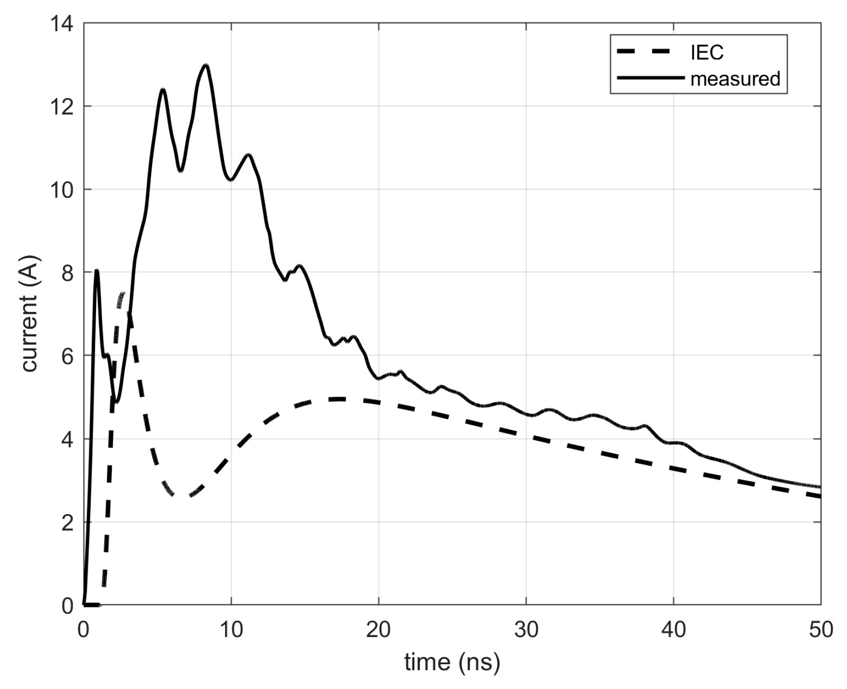
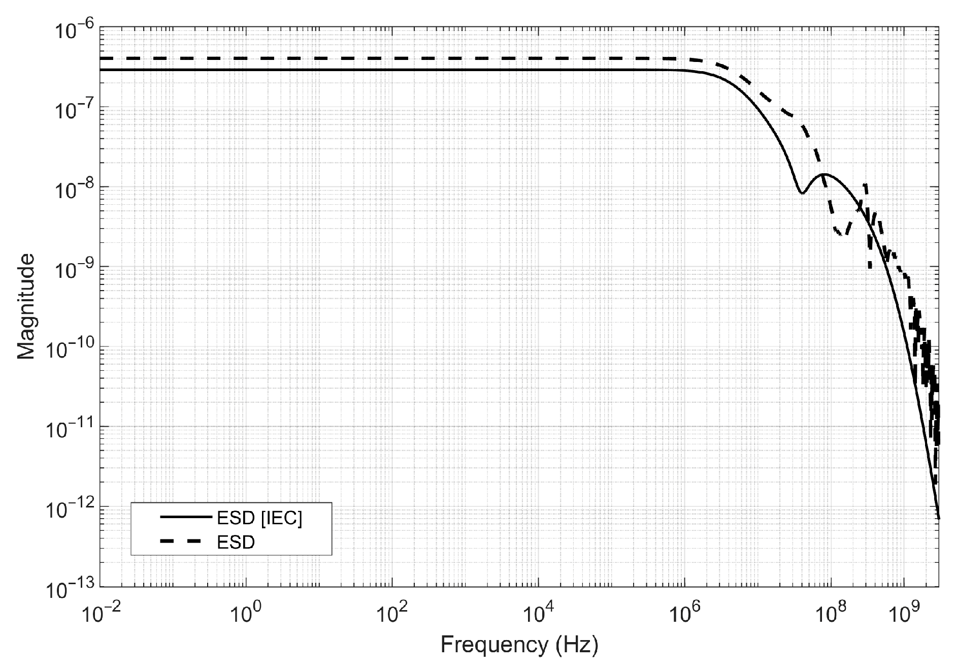
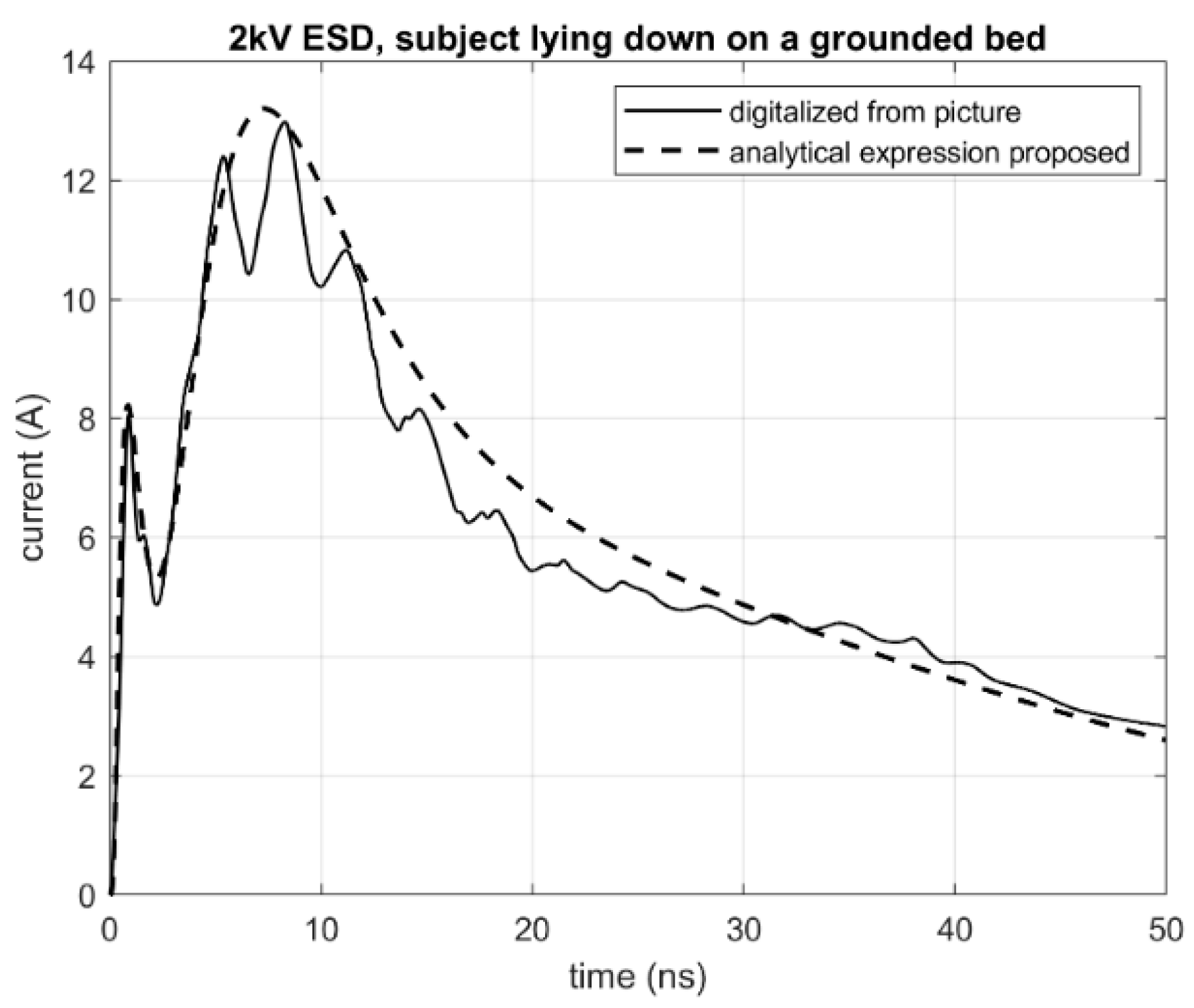
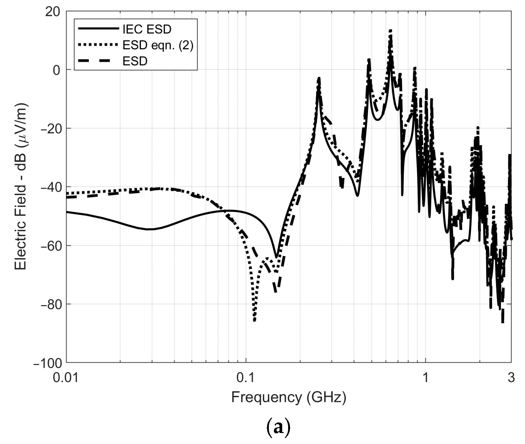
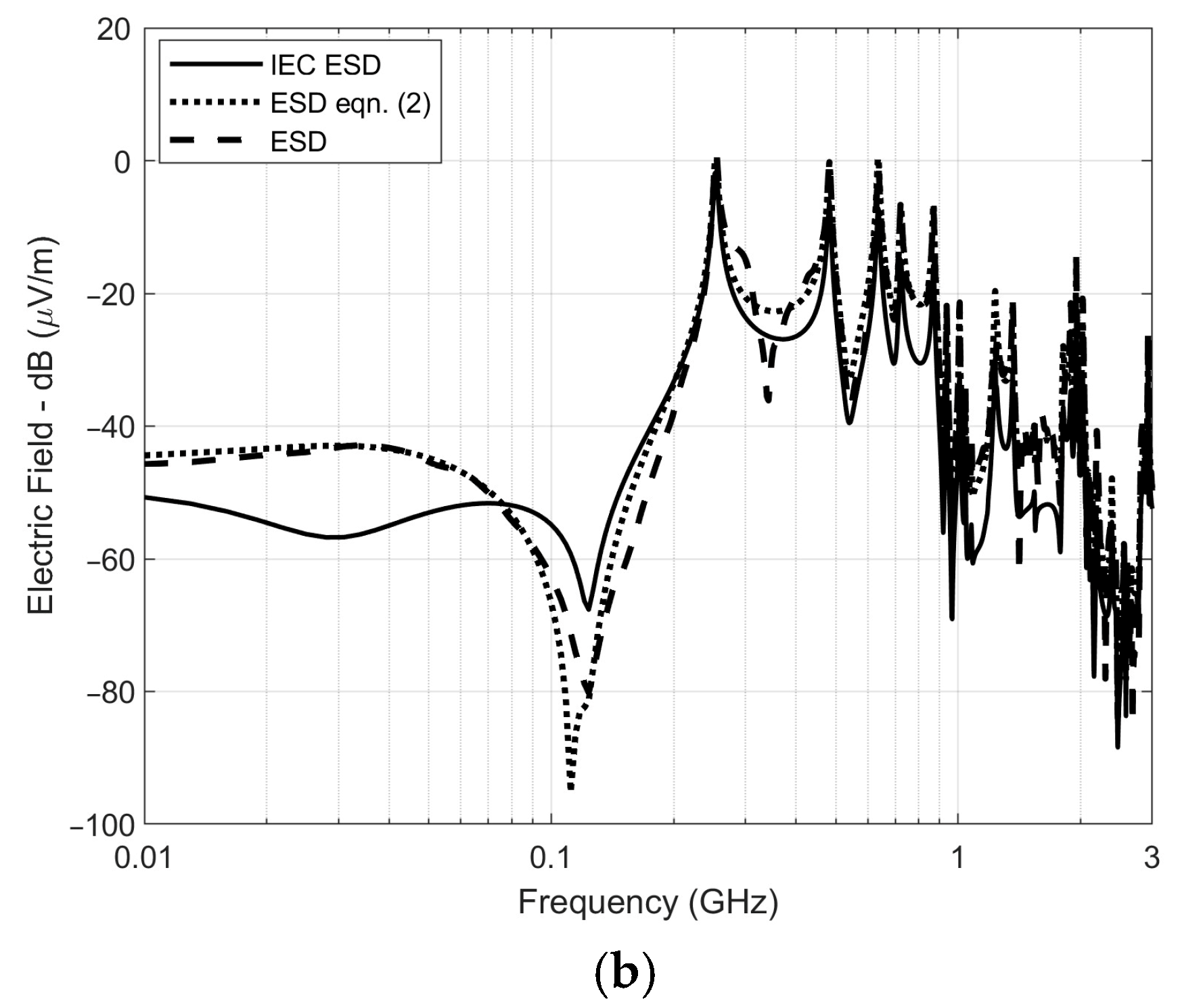
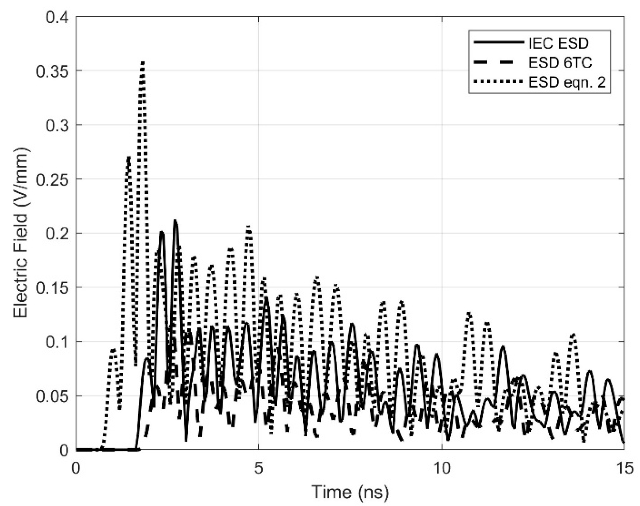
This model is 2 kV ESD, considering a subject lying down on a grounded bed [28], with air discharge. This waveform has been numerically digitalized from the measured data and is seen in Figure 2 where the standard IEC 61000-4-2 for the same voltage drop is also reported for comparison and to demonstrate that a current much larger than that reported by the standard may occur in practice. Figure 3 reports the corresponding frequency spectra, and they are similar, despite the remarkable differences in the time domain, apart from a larger frequency content above some hundreds of MHz.
An analytical fitting of these measured data is proposed here, adopting an approach similar to that proposed in [26], as Figure 4 shows, where the comparison between the measured waveform and the analytical fitting is reported. The fitting is obtained by means of the new following expression, with values of the relevant parameters (i.e., six time constants τk, with k = 1,…,6; three current amplitudes, I0, I1, I2; three fitting exponents, p, q, r) reported in Table 3.
i ( t ) = I 0 1 e t τ 1 p · e t τ 2 + I 1 1 e t τ 3 q · e t τ 4 + I 2 1 e t τ 5 r · e t τ 6
The comparison between waveforms in Figure 2 provides evidence that actual ESD may present a risetime shorter than that recommended by the IEC standard, with a double (multiple) peak occurrence. As a consequence, the frequency spectrum has a higher content above a few hundred MHz, with respect to the IEC waveform. Figure 3 shows this, in which the frequency spectra is reported on a logarithmic scale.

2.2. Physical Source Numerical Modeling

The simulation of the source has been pursued by means of a numerical approach [29,30,31,32,33]: a transient lumped current source (with internal impedance of 50 Ω, length 0.5 mm, radius = 0.5 mm) is placed in the middle between the central point of a microstrip line (W = 1 mm, L = 49.5 mm, placed at a distance of 25 cm from another microstrip line with W = 1 mm, L = 50 mm) and the center point of the ground plane (W = L = 50 mm). The ground plane is modeled as a perfect electric conductor, while copper is considered for the microstrip lines. Some details and improvements of the original model were presented in [34,35].
An alternative approach based on neural networks and aimed at determining the incident field due to an indirect ESD has been proposed in [36], but in this case a fully numerical method has been preferred because of the need to also simulate the victim.

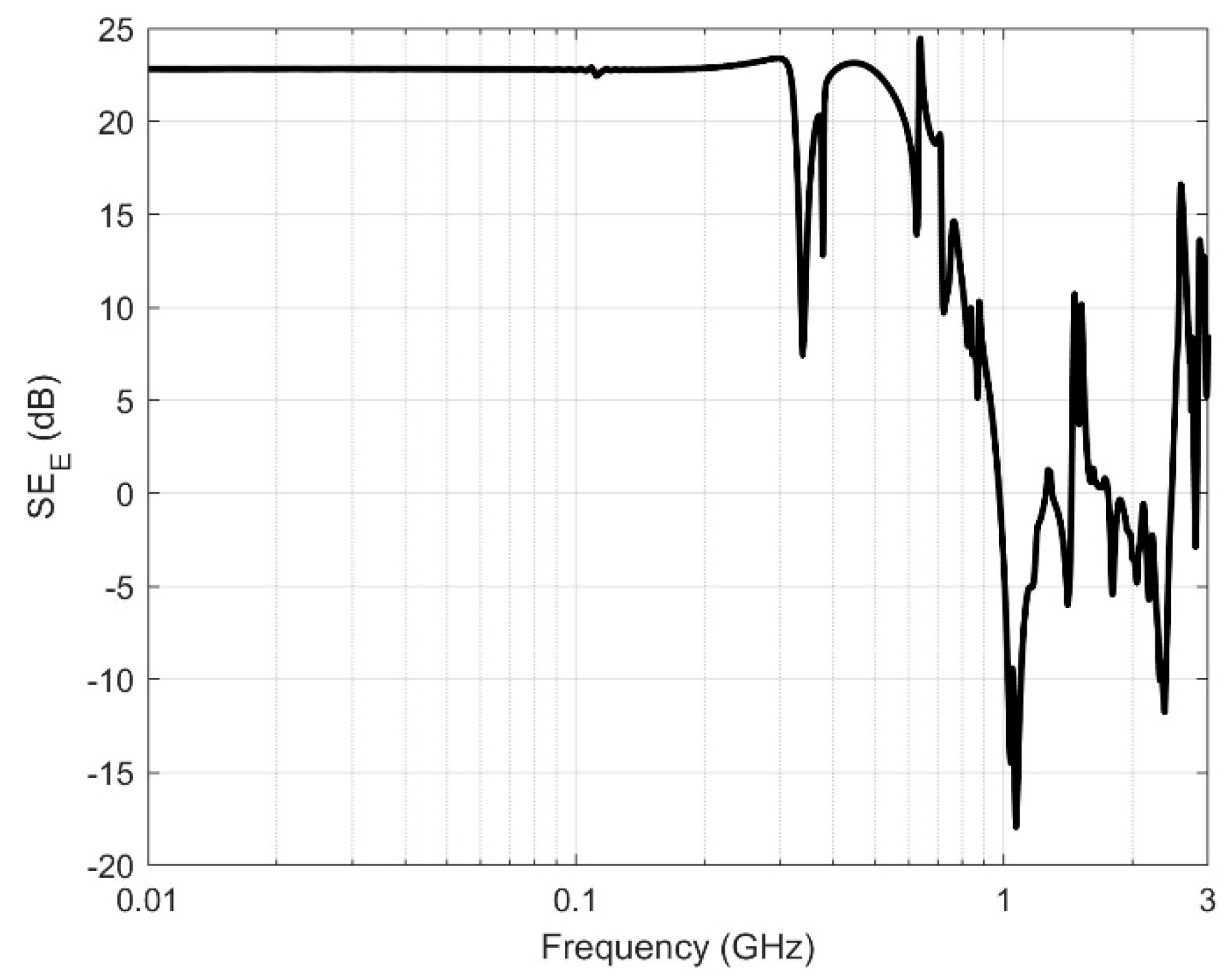
3. Shielding Performance of a Planar Grid

In the past [37], it has been demonstrated that the numerical prediction of the shielding performance in the case of a planar perforated shield is reliable, and it compares well with measured data. Recently, in the same canonical configuration, the influence of various geometrical and physical parameters, and that of the source modeling, have been thoroughly investigated [38], recording evidence of the important differences ensuing from the choice of the characteristics of the considered victim. In the following example, the influence of the grid dimensions on the shielding performance is evaluated in terms of the electric or magnetic field attenuation.
The source is an ESD occurring at a distance of 30 mm from a conductive planar shield (Figure 5a) where a square grid of square apertures is present (Figure 5b). The observation point is symmetrical to the source with respect to the shield. Of course, the larger the dimensions of the grid the lower the shielding performance is, as Figure 6 shows, with a minimum value of about 20–25 dB around 400–600 MHz.
However, such information about the shielding performance in planar configurations is unsuitable for the prediction of the field incident on victims protected by enclosures with apertures, as will be shown in the next section, where the numerical approach is exploited to accurately simulate apertures having different dimensions and irregular spacing among those.

4. Numerical Simulations of Shielding Enclosures

Two typical configurations have been selected to investigate the susceptibility to ESD of components installed in an MV/LV substation. The first is a mini computing unit suitable for elaborating and transmitting relevant data for the status of a smart grid. The second component is a typical electronic protection relay (often referred to as an IED, intelligent electronic device).

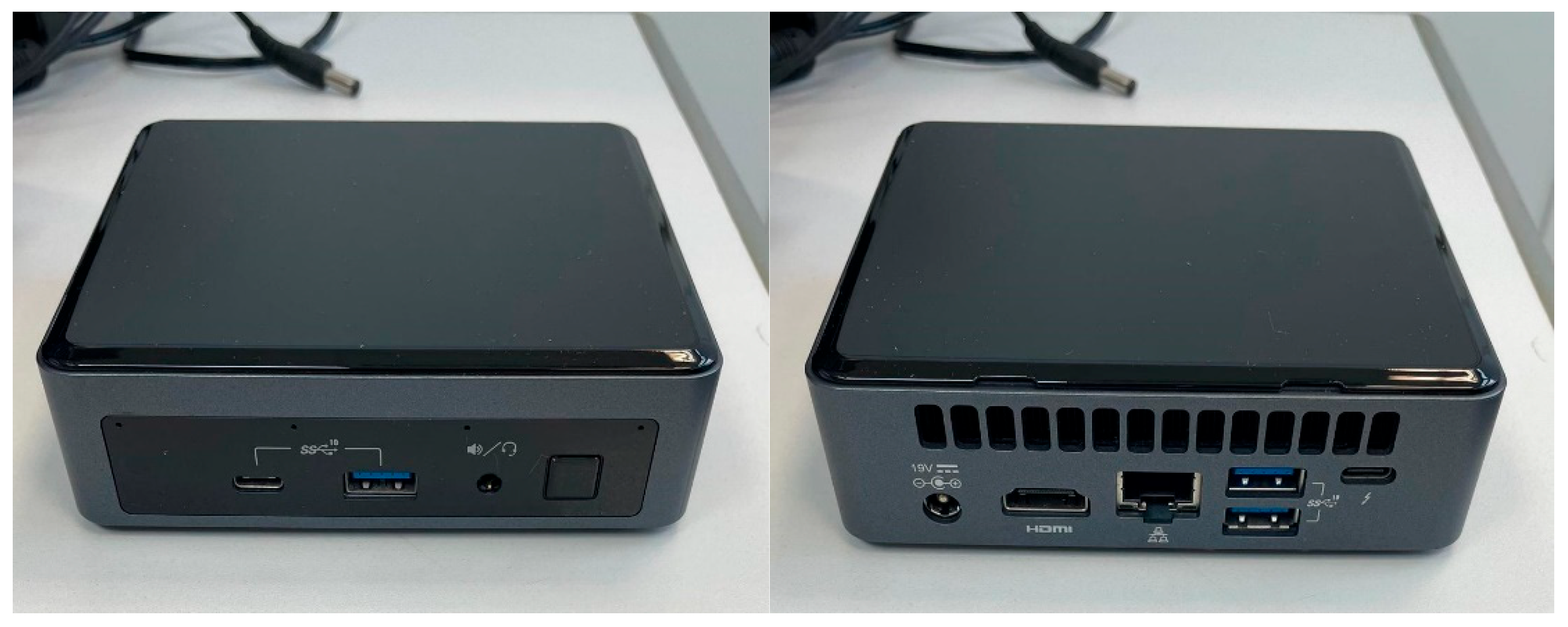
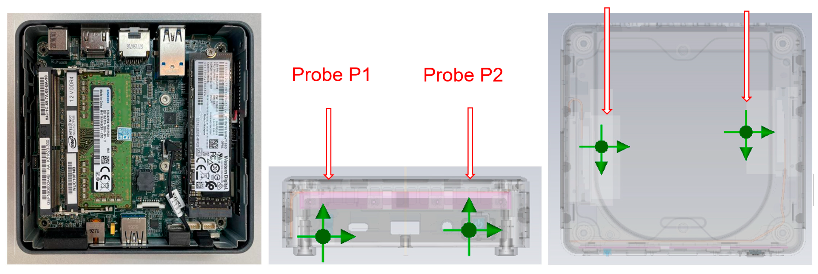
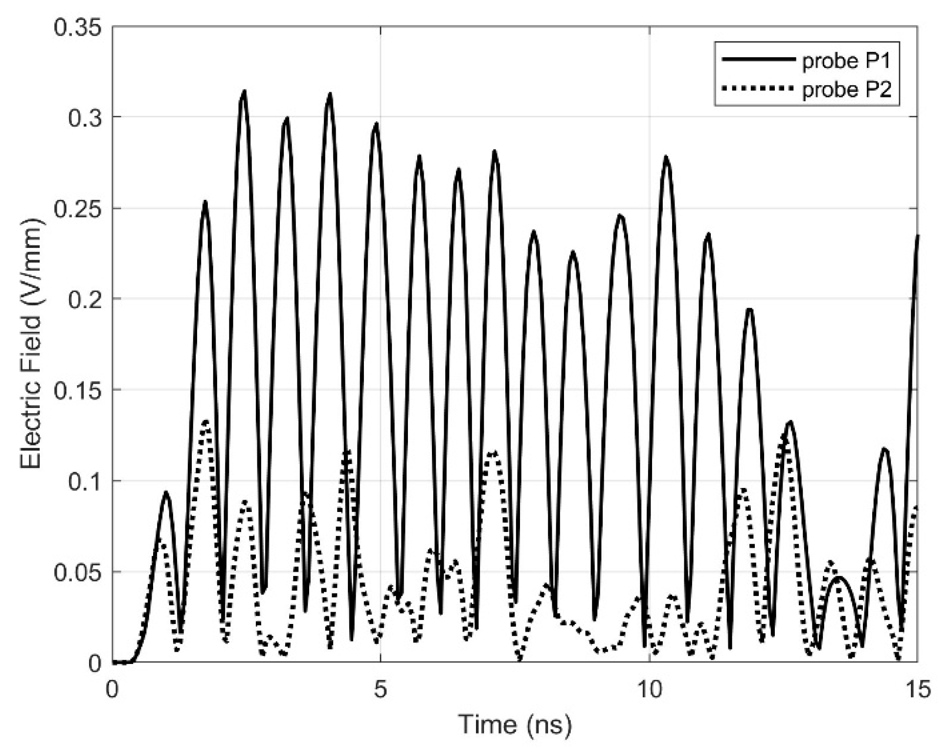
4.1. First Device Under Test: Mini Computing Unit

The first configuration considered is a real device, available on the market and often adopted for processing and transmitting the data collected by the various measurement apparatus and sensors equipping an MV/LV substation.
Such a tiny PC (in our test an Intel (Santa Clara, CA, USA) NUC, Next Computing Unit model NUC10i7FNK [39]) has a variety of apertures for ventilation and for cable input/output connections: three USB-3 ports, two USB type C ports, one HDMI interface, one RJ-45 connector, one microphone jack, a ventilation grid, and a connector for the dc adapter. The arrangement of the apertures depends on the layout of the internal components and therefore does not follow a well-defined geometric pattern. Figure 7 shows the device, and its 3D drawing has been imported into CST Studio Suite [40]:
external dimensions: 112.6 mm × 117 mm × 37.7 mm;
a total of 64 types of different internal components;
discretization: 24,000,000 tetrahedral mesh cells.
In Figure 8 the details of the exterior of the imported geometry are also shown, while Figure 9 shows the actual content of the enclosure with the positions of the two considered observation points indicated by red arrows.
Classical open boundary conditions have been applied. The discretization has been increased until the results remained practically constant.
The observation points have been located in an almost symmetrical position with respect to the pulse source, in particular: the left probe (P1, located at x = −39 mm, y = 9 mm, z = −53 mm, being the x-axis origin at the center of the enclosure, the y-axis coordinate is 0 at the bottom, and z = 0 is on the front surface) is close to the SSD M.2 disk (supply voltage 3.3 V), and the right one (P2, located at x = 30 mm, y = 12 mm, z = −60 mm) is near the RAM (supply voltage 1.2 V).
The ESD source has been positioned at 30 mm from the front side of the device being tested to simulate a discharge occurring between a charged body and the open metallic rack where generally the device being tested is placed.
In Figure 10a,b the frequency spectra of the electric field in the two observation points P1 and P2 are shown, evaluated as a consequence of the time domain results reported in Figure 11. Units have been set in V/mm for an immediate comparison and appraisal of the possible interference with typical signals involving the two susceptible components close to the observation points.
In fact, the relevant pins of the two potential victims are far from each other, being about 0.5–1 mm away, and thus, an additional waveform, whose maximum value is comparable with the nominal signals, is surely harmful [41] for the correct functioning of the device being tested.
It should be noted that such a small enclosure is not covered by the relevant IEEE Std. 299-1 [17] because its dimensions are less than 0.1 m. Moreover, the case is so full of components that the insertion of test probes is not feasible; however, measurements conducted in a void enclosure, apart from the difficulties arising from the capacitive coupling with the case, are not representative of the EM behavior as described in the cited standard. Figure 12 presents the shielding effectiveness of the enclosure, and some resonances are present: at these frequencies, the electric field inside the enclosure being tested is higher than that observed in the absence of the enclosure.
Furthermore, hardware/software failures/damages depend also on the level of the applied ESD voltage, which, in the following examples, has been fixed at its minimum value equal to 2 kV in order to ascertain whether even the less severe ESD might be potentially harmful.
Moreover, it is interesting to analyze the significant differences existing between the EM fields in the two observation points. In the time domain, the most important peaks in P1 are up to four times greater than the corresponding peaks observed in P2. In the frequency domain, in both of the observation points, the most critical frequencies are characterized by almost the same level of enhancement of the field with respect to the incident value (evaluated in the absence of the enclosure).
In Figure 13 the maps ensuing from an ESD described by (2) are reported, considering the three planes passing through the observation point P1, while in Figure 14 the cut planes are those passing through P2. The electric field maps are plotted at the time instant when the current exhibits its peak value.
Several areas exhibit an electric field in the order of 1 V/mm, capable of interfering with the normal operating conditions of most electronic devices. This occurrence is more pronounced at the lower level of the y-coordinate (y = 9 mm) with respect to y = 12 mm, i.e., the SSD is more solicited than RAM. “Quiet” areas are also present: there the perturbation caused by a frontal ESD is practically irrelevant and the installation of sensitive components is convenient.
When analyzing Figure 13 and Figure 14 in detail it is possible to note the effects of metal bodies: at their sharp corners, an enhancement of the electric field occurs, as evident, e.g., in the x-y plane cut of Figure 13 and Figure 14 (at the bottom, on the left). As a consequence, the possible insertion of a partial shield to protect some specific components would increase the EM field in the area immediately adjacent to the protected one.

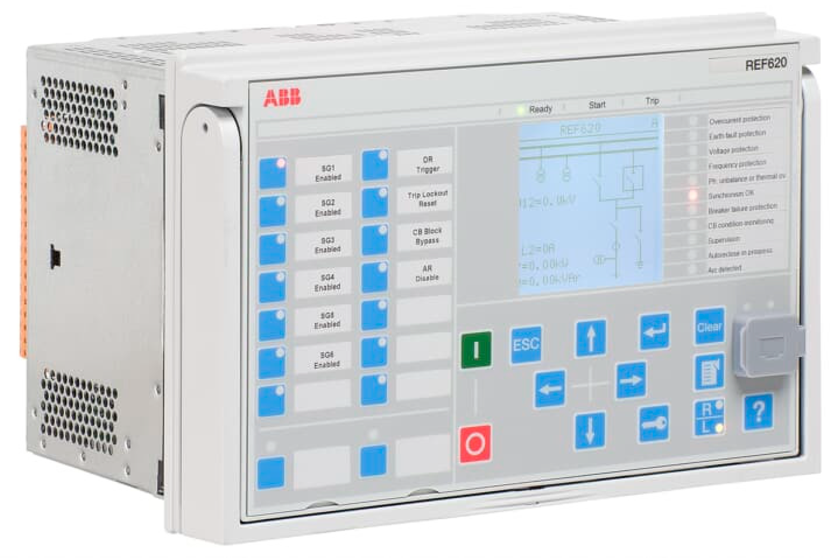
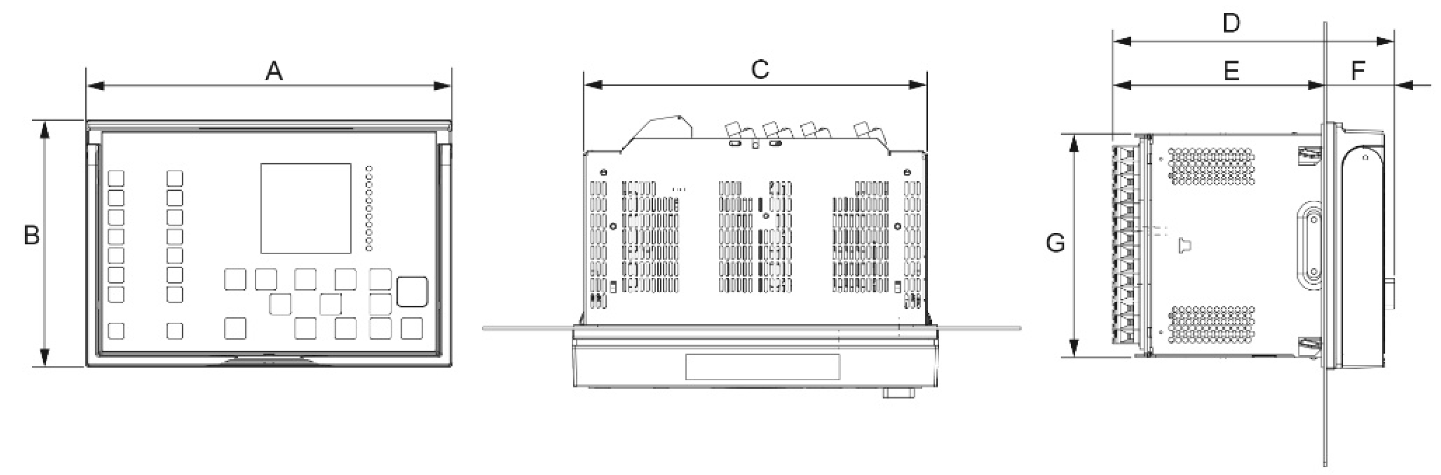
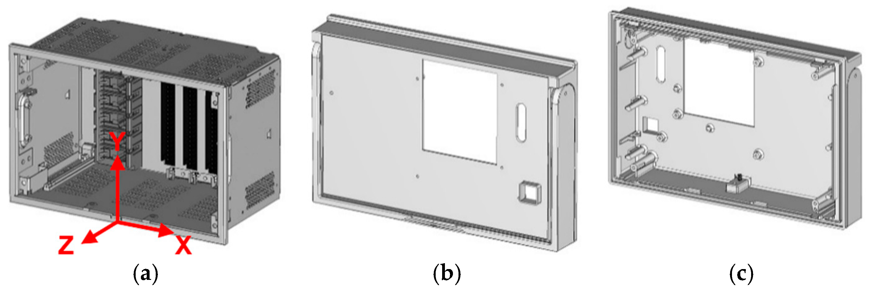
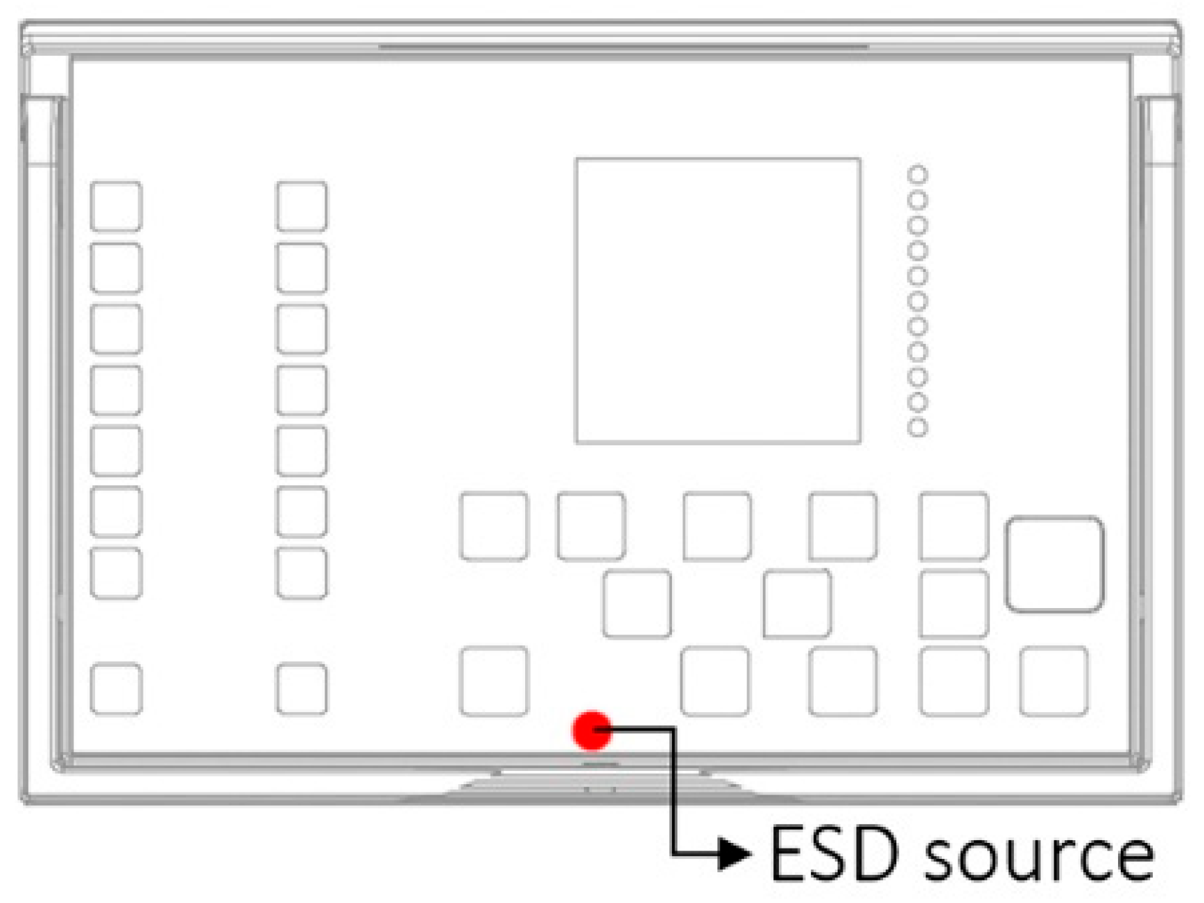
4.2. Second Device Under Test: Relay Model ABB REF 620

The second device being tested is a dedicated feeder management relay for protection, control, measurement, and supervision in utility and industrial power distribution systems [42,43]; the ABB (Zurich, Switzerland) model REF 620, as shown in Figure 15, Figure 16 and Figure 17, has been considered because of its large diffusion. The dimensions are larger than the minimum allowed by IEEE Std. 299.1; however, the room within the enclosure is not large enough to host a receiving antenna, thus, numerical investigation is the only feasible way to approach the analysis.
Once the 3D drawing of ABB REF 620 has been imported into CST Studio Suite, and a discretization of the domain is performed, one obtains the following:
external dimensions: 262.2 mm × 177 mm × 201 mm;
properties: 137 internal solids—11 different materials;
discretization: approximately 183,000,000 tetrahedral mesh cells.
Although the external dimensions are all larger than 0.1 m, standard 299.1 is not applicable because the internal volume is smaller, and, thus, sensors or antennas cannot be inserted inside the shielded volume.
For this simulation, the probe has been positioned in the middle of the case, close to the printed circuit board where the electronic components at the basis of the relay operation are installed.
The ESD source is placed 30 mm from the front of the REF 620, in correspondence to the keys, where a charged finger will very likely approach the device. Figure 18 shows this configuration.
Figure 19 shows the electric field computed at the observation point for the different waveforms already considered. Again, the ESD waveform recently measured, as in [28], may yield to a threat significantly more severe than that commonly considered according to the standards, either in terms of the field peak value and in terms of the time derivative.
As can be noticed, the values of the electric field may generate harmful signals, in terms of voltage drops, between pins whose distance is in the order of 1 mm. As well, by analyzing Figure 20 it can be observed that internal reflections may yield to negative values of the shielding effectiveness [44,45,46,47] at some frequency intervals.
In the following Figure 21, the maps ensuing from an ESD described by (2) are reported, considering the three planes passing through the observation point. The electric field maps are plotted in correspondence of the time instant in which the current exhibits its peak value. It is interesting to observe that the order of magnitude of the voltage drop between two pins due to an ESD at some positions may reach levels comparable with the normal signals, determining possible malfunctioning conditions or even failures.
In this latter configuration, the most critical area is that close to the large aperture hosting the graphical display unit: in its proximity is the printed circuit board and such a reduced distance (about 15 mm) may represent a risk factor for the electronic components of the relay.
Some general remarks may be obtained from the two particular cases analyzed, which are as follows:
-
very often the apertures shape and position are determined by functional constraints and no (or very limited) degrees of freedom exist at the design stage, apart from their possible interchanging;
-
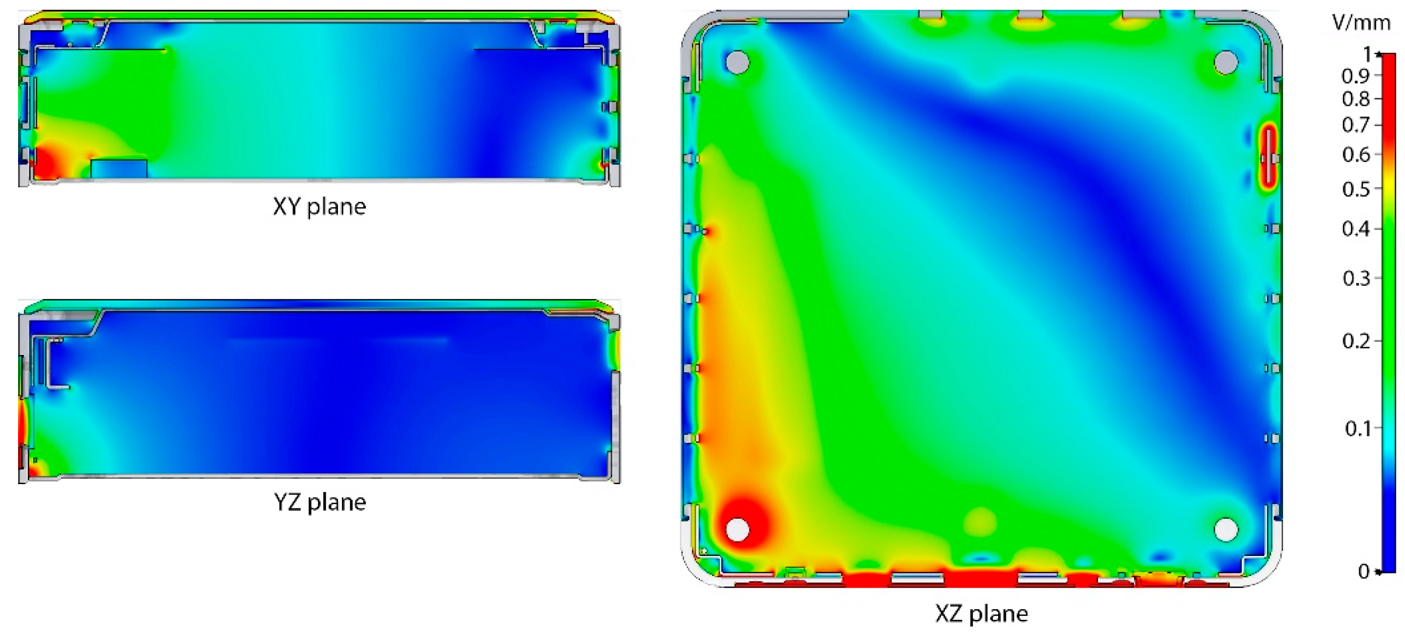
the EM field distribution inside the enclosure is highly non-uniform and strongly dependent on the presence of components, especially metallic ones, i.e., loaded actual enclosures behave very differently from empty ones;
-
as a consequence, inferring general conclusions from the analysis of ideal configurations is potentially misleading, especially if they refer to simplified enclosure geometries or void protected volumes;
-
great attention should be paid to metallic bodies (like screws [48,49], heatsinks [50,51], pins, connectors [52,53], etc.) inside the enclosure: they can re-radiate the impinging EM field and often present some high-intensity field areas near sharp corners;
-
due to the very large number of degrees of freedom associated with the positioning of the main components inside the enclosure, it is suggested that the design stage should be divided into five phases to be faced with on a case-by-case basis, i.e., considering actual configurations and not ideal ones, void enclosures.
(1) As such, consider first the most convenient configuration from a functional point of view for both apertures and internal components (including electronic and structural metallic bodies like screws and heatsinks);
(2) analyze the EM field distribution and check whether the induced effects on the most important components (this individuation requires a separate investigation) are harmful or not.
If some critical situations occur then do the following:
(3) design some partial internal shields around the areas identified as critical and/or,
(4) explore the positioning of the most susceptible components in the “quite” areas,
(5) analyze again (and eventually repeat phases 3–5 if necessary).
Finally, it can be observed that conducting all the investigations in the time domain is convenient because it is very difficult to estimate the peak level (and the time derivative of the waveforms, when they are relevant) of induced effects from frequency domain masks.

5. Conclusions

In this paper, two main issues concerning the shielding performance of small enclosures (i.e., those whose dimensions are smaller than 0.1 m) have been investigated considering an ESD as the electromagnetic field source:
(a)
the accurate modeling of the enclosure taking into account the exact shape and position of all the apertures and that of all the internal metallic and/or dielectric parts;
(b)
the influence of the internal components (loading) on the electromagnetic field distribution.
The results ensuing from a numerical procedure aimed at assessing the effects of an ESD on two typical devices installed in MV/LV substations have been presented. In fact, because of the absence of space to host a receiving antenna or sensor, no experimental tests may be conducted in loaded enclosures; moreover, the limited dimensions of the devices being tested do not allow for the insertion of sensors into their void enclosures while avoiding coupling with the walls and the internal components, making the measurements largely inaccurate. On the contrary, numerical predictions have been demonstrated to be reliable in a number of similar configurations.
In particular, the less severe discharge current waveform described by standards has been considered, i.e., that associated with a 2 kV voltage drop existing between the extremities of the arc, by proposing a new analytical waveform stemming from experimental data available in the literature. The two typical devices were analyzed: a mini computer unit, and a relay for protection and control of the distribution network. In both cases, the exact layout of internal components and the characteristics (either physical and geometrical for, respectively, more than 60 and more than 130 different bodies) have been simulated in order to accurately account for the actual behavior of the most critical devices.
As a result of this investigation, it has been demonstrated that:
(a)
ESD is a potentially harmful event which should be considered in the protection of devices installed in modern MV/LV substations where electronic components are tightly linked with proper functionality of the distribution network;
(b)
a numerical investigation is suitable for the accurate appraisal of the electromagnetic performance of shielding enclosures, allowing for their complex geometries and content to be taken into account;
(c)
an informed positioning of the most critical victims inside enclosures is useful to avoid areas where the electromagnetic field is more intense due to the non-uniform field distribution.

Author Contributions

Software, methodology, investigation, formal analysis, and visualization, G.A.; conceptualization, investigation, writing—original draft preparation, and supervision, S.C.; formal analysis, and writing—review and editing, E.S. All authors have read and agreed to the published version of the manuscript.

Funding

This research received no external funding.

Data Availability Statement

The dataset is available on request from the authors.

Conflicts of Interest

The authors declare no conflicts of interest.

References

  1. Voldman, S.H. The ESD Handbook; John Wiley & Sons: Hoboken, NJ, USA, 2021. [Google Scholar]
  2. Mardiguian, M. Electrostatic Discharge: Understand, Simulate, and Fix ESD Problems; John Wiley & Sons: Hoboken, NJ, USA, 2011. [Google Scholar]
  3. Holdstock, P. A review of electrostatic standards. J. Electrost. 2022, 115, 103652. [Google Scholar] [CrossRef]
  4. Concannon, A. Evolution of ESD Robust IC Design: How ESD design and ESD control have changed our industry. IEEE Solid-State Circuits Mag. 2023, 15, 58–63. [Google Scholar] [CrossRef]
  5. Zhang, J.; Zeng, D.; Feng, D.; Liao, J.; Chen, Z.; Ding, R.; Zhou, R.; Chen, J.; Shao, W. Testing and Analysis of DC/DC Circuit Boards Based in ESD Interference Sources. In Proceedings of the 2024 IEEE 7th International Conference on Electronic Information and Communication Technology (ICEICT), Xi’an, China, 31 July–2 August 2024; IEEE: Piscataway, NJ, USA, 2024; pp. 362–365. [Google Scholar]
  6. Gizatullin, Z.; Shkinderov, M. Increasing the noise immunity of the access monitoring and control system under the influence of electrostatic discharge. In Proceedings of the 2021 International Conference on Industrial Engineering, Applications and Manufacturing (ICIEAM), Sochi, Russia, 17–21 May 2021; IEEE: Piscataway, NJ, USA, 2021; pp. 515–519.
  7. Keebler, P.F. Meshing power quality and electromagnetic compatibility for tomorrow’s smart grid. EEE Electromagn. Compat. Mag. 2012, 1, 100–103. [Google Scholar] [CrossRef]
  8. Kulikov, A.; Loskutov, A.; Bezdushniy, D. Relay Protection and Automation Algorithms of Electrical Networks Based on Simulation and Machine Learning Methods. Energies 2022, 15, 6525. [Google Scholar] [CrossRef]
  9. Majeed, A.A.; Altaie, A.S.; Abderrahim, M.; Alkhazraji, A. A Review of Protection Schemes for Electrical Distribution Networks with Green Distributed Generation. Energies 2023, 16, 7587. [Google Scholar] [CrossRef]
  10. Hasan, M.K.; Habib, A.A.; Islam, S.; Balfaqih, M.; Alfawaz, K.M.; Singh, D. Smart Grid Communication Networks for Electric Vehicles Empowering Distributed Energy Generation: Constraints, Challenges, and Recommendations. Energies 2023, 16, 1140. [Google Scholar] [CrossRef]
  11. Kaleybar, H.J.; Brenna, M.; Foiadelli, F.; Fazel, S.S.; Zaninelli, D. Power Quality Phenomena in Electric Railway Power Supply Systems: An Exhaustive Framework and Classification. Energies 2020, 13, 6662. [Google Scholar] [CrossRef]
  12. IEC TS 60079-32-1; Explosive Atmospheres—Part 32-1: Electrostatic Hazards, Guidance. IEC: Geneva, Switzerland, 2013.
  13. IEC 61340-5-1:2024; Electrostatics—Part 5-1: Protection of Electronic Devices from Electrostatic Phenomena—General Requirements. IEC: Geneva, Switzerland, 2024.
  14. Hyatt, H. ESD: Standards, Threats and System Hardness Fallacies. In Proceedings of the 2002 Electrical Overstress/Electrostatic Discharge Symposium, Charlotte, NC, USA, 6–10 October 2002; IEEE: Piscataway, NJ, USA, 2002; pp. 178–185. [Google Scholar]
  15. Stepins, D.; Asmanis, A.; Asmanis, G.; Ribickis, L.; Audze, J. Effect of Shielding and Component Placement in DM EMI Filters on a Power Supply’s Conducted EMI. In Proceedings of the 2018 20th European Conference on Power Electronics and Applications (EPE’18 ECCE Europe), Riga, Latvia, 17–21 September 2018; pp. P.1–P.5. [Google Scholar]
  16. Joshi, M.; Agarwal, V. Component placement for improved EMI performance in power electronic circuits. In Proceedings of the APEC’98 Thirteenth Annual Applied Power Electronics Conference and Exposition, Anaheim, CA, USA, 15–19 February 1998; IEEE: Piscataway, NJ, USA, 1998; Volume 2, pp. 911–917. [Google Scholar]
  17. IEEE 299.1-2013; IEEE Standard Method for Measuring the Shielding Effectiveness of Enclosures and Boxes Having All Dimensions between 0.1 m and 2 m. IEEE: Piscataway, NJ, USA, 15 January 2014. [CrossRef]
  18. Bergsma, H.; Clemens, C.; Leferink, F. Shielding Effectiveness of Cabinets using IEEE 299 and IEEE 299.1 and Effect of Loading. In Proceedings of the 2022 International Symposium on Electromagnetic Compatibility—EMC Europe, Gothenburg, Sweden, 5–8 September 2022; pp. 59–63. [Google Scholar]
  19. Kubík, Z.; Skála, J. Shielding effectiveness simulation of small perforated shielding enclosures using FEM. Energies 2016, 9, 129. [Google Scholar] [CrossRef]
  20. Budnarowska, M.; Mizeraczyk, J.; Bargieł, K. Development of the EM Field in a Shielding Enclosure with Aperture after Interference Caused by a Subnanosecond High-Power Parallelly Polarized EM Plane Wave Pulse. Energies 2023, 16, 585. [Google Scholar] [CrossRef]
  21. Budnarowska, M.; Mizeraczyk, J. Determination of shielding effectiveness of a subnanosecond high-power EM interference by an enclosure with aperture using time domain approach. Energies 2023, 16, 1931. [Google Scholar] [CrossRef]
  22. Chen, Z.; Catrysse, J.; Claeys, T.; Pissoort, D. Evaluation of Shielding Effectiveness of Physically Small Enclosures Using Different Types of Receiving Antennas via Full-wave Simulation. In Proceedings of the 2024 International Symposium on Electromagnetic Compatibility–EMC Europe, Bruges, Belgium, 2–5 September 2024; IEEE: Piscataway, NJ, USA, 2024; pp. 612–616. [Google Scholar]
  23. Marvin, A.C.; Dawson, J.F.; Ward, S.; Dawson, L.; Clegg, J.; Weissenfeld, A. A proposed new definition and measurement of the shielding effect of equipment enclosures. IEEE Trans. Electromagn. Compat. 2004, 46, 459–468. [Google Scholar] [CrossRef]
  24. Flintoft, I.D.; Bale, S.J.; Marvin, A.C.; Ye, M.; Dawson, J.F.; Wan, C.; Zhang, M.; Parker, S.L.; Robinson, M.P. Representative contents design for shielding enclosure qualification from 2 to 20 GHz. IEEE Trans. Electromagn. Compat. 2017, 60, 173–181. [Google Scholar] [CrossRef]
  25. IEC 61000-4-2; EMC—Part 4-2: Testing and Measurement Techniques—Electrostatic Discharge Immunity Test. IEC: Geneva, Switzerland, 2009.
  26. Yuan, Z.; Li, T.; He, J.; Chen, S.; Zeng, R. New mathematical descriptions of ESD current waveform based on the polynomial of pulse function. IEEE Trans. Electromagn. Compat. 2006, 48, 589–591. [Google Scholar] [CrossRef]
  27. Javor, V. New Function for Representing IEC 61000-4-2 Standard Electrostatic Discharge Current; Series: Electronics and Energetics; Facta Universitatis: Niš, Serbia, 2014; Volume 27, pp. 509–520. [Google Scholar] [CrossRef]
  28. Kohani, M.; Meiguni, J.; Pommerenke, D.J.; Pecht, M.G. ESD Events to Wearable Medical Devices in Healthcare Environments—Part 1: Current Measurements. IEEE Trans. Electromagn. Compat. 2023, 65, 954–959. [Google Scholar] [CrossRef]
  29. Katsivelis, P.K.; Fotis, G.P.; Gonos, I.F.; Koussiouris, T.G.; Stathopulos, I.A. Electrostatic discharge current linear approach and circuit design method. Energies 2010, 3, 1728–1740. [Google Scholar] [CrossRef]
  30. Zhang, J.; Beetner, D.G.; Moseley, R.; Herrin, S.; Pommerenke, D. Modelling electromagnetic field coupling from an ESD gun to an IC. In Proceedings of the 2011 IEEE International Symposium on Electromagnetic Compatibility, Long Beach, CA, USA, 14–19 August 2011; IEEE: Piscataway, NJ, USA, 2011; pp. 553–558. [Google Scholar]
  31. Fotis, G. Electromagnetic fields radiated by electrostatic discharges: A review of the available approaches. Electronics 2023, 12, 2577. [Google Scholar] [CrossRef]
  32. Pommerenke, D. ESD: Transient fields, arc simulation and rise time limit. J. Electrost. 1995, 36, 31–54. [Google Scholar] [CrossRef]
  33. Wang, K.; Pommerenke, D.; Chundru, R.; Van Doren, T.; Drewniak, J.L.; Shashindranath, A. Numerical modeling of electrostatic discharge generators. IEEE Trans. Electromagn. Compat. 2003, 45, 258–271. [Google Scholar] [CrossRef]
  34. Marathe, S.; Li, D.; Hosseinbeig, A.; Rezaei, H.; Wei, P.; Zhou, J.; Pommerenke, D. On secondary ESD event monitoring and full-wave modeling methodology. In Proceedings of the 2017 39th Electrical Overstress/Electrostatic Discharge Symposium (EOS/ESD), Tucson, AZ, USA, 10–14 September 2017; IEEE: Piscataway, NJ, USA, 2017; pp. 1–6. [Google Scholar]
  35. Luo, G.X.; Huang, B.C.; Huang, K.; Mi, R.; Pommerenke, D. Human Metal ESD: Design of a Full-Wave Model and an Improved Compact Generator. IEEE Trans. Electromagn. Compat. 2023, 65, 634–642. [Google Scholar] [CrossRef]
  36. Ekonomou, L.; Fotis, G.P.; Maris, T.I.; Liatsis, P. Estimation of the electromagnetic field radiating by electrostatic discharges using artificial neural networks. Simul. Model. Pract. Theory 2007, 15, 1089–1102. [Google Scholar] [CrossRef]
  37. Araneo, R.; Lovat, G.; Celozzi, S. Shielding effectiveness of periodic screens against finite high-impedance near-field sources. IEEE Trans. Electromagn. Compat. 2011, 53, 706–716. [Google Scholar] [CrossRef]
  38. Attolini, G.; Celozzi, S.; Stracqualursi, E. Influence of the Experimental Setup on the Shielding Performance of Perforated Grids Against an Indirect Electrostatic Discharge. In Proceedings of the 2024 IEEE International Conference on Environment and Electrical Engineering and 2024 IEEE Industrial and Commercial Power Systems Europe (EEEIC/I&CPS Europe), Rome, Italy, 17–20 June 2024; IEEE: Piscataway, NJ, USA, 2024; pp. 1–6. [Google Scholar]
  39. Intel NUC Products NUC10i3FN, NUC10i5FN and NUC10i7FN Technical Product Specification; Intel Corporation: Santa Clara, CA, USA, 2021.
  40. CST Studio Suite, version 2024.02; Software for electromagnetic field computation; Dassault Systèmes: Vélizy-Villacoublay, France, 2025.
  41. ABB Relion® Protection and Control 620 Series Installation Manual; ABB Nanjing SAC Power Grid Automation Co., Ltd.: Nanjing, China, 2019.
  42. ABB Relion® Protection and Control 620 series ANSI Installation Manual; ABB Inc.: Lake Mary, FL, USA, 2019.
  43. Hwang, J.H.; Park, H.H.; Hyoung, C.H.; Kwon, J.H. Consistent shielding effectiveness measurements for small enclosures in reverberation and semianechoic chambers. IEEE Trans. Instrum. Meas. 2022, 71, 1–13. [Google Scholar] [CrossRef]
  44. Celozzi, S.; Araneo, R. TD-Shielding effectiveness of enclosures in presence of ESD. In Proceedings of the 2013 IEEE International Symposium on Electromagnetic Compatibility, Denver, CO, USA, 5–9 August 2013; pp. 541–544. [Google Scholar]
  45. Araneo, R.; Attolini, G.; Celozzi, S.; Lovat, G. Time-domain shielding performance of enclosures: A comparison of different global approaches. IEEE Trans. Electromagn. Compat. 2016, 58, 434–441. [Google Scholar] [CrossRef]
  46. Duvvury, C.; Gossner, H. (Eds.) System Level ESD Co-Design; John Wiley & Sons: Hoboken, NJ, USA, 2015. [Google Scholar]
  47. Yousaf, J.; Faisal, M.; Youn, J.; Nah, W. Design of Experiment (DOE) Analysis of System Level ESD Noise Coupling to High-Speed Memory Modules. Electronics 2019, 8, 210. [Google Scholar] [CrossRef]
  48. Chen, L.; Ning, F.; Jiao, C. Research on the influence of screw spacing on magnetic shielding effectiveness of a shielding cabin. In Proceedings of the E3S Web of Conferences, Virtual, 22–24 July 2020; EDP Sciences: Les Ulis, France, 2020; Volume 185, p. 01083. [Google Scholar]
  49. Kunkel, G.M. Shielding of Electromagnetic Waves; Springer International Publishing: Cham, Switzerland, 2020. [Google Scholar]
  50. Jin, H.; Zhang, L.; Yang, X.L.; Cheng, P.; Li, E.P.; Zhang, Y.J. A novel heatsink with mushroom-type EBG structure for EMI radiation suppression. In Proceedings of the 2018 IEEE International Symposium on Electromagnetic Compatibility and 2018 IEEE Asia-Pacific Symposium on Electromagnetic Compatibility (EMC/APEMC), Singapore, 14–18 May 2018; IEEE: Piscataway, NJ, USA, 2018; pp. 772–775. [Google Scholar]
  51. Genc, A.; Helhel, S. The comparison of em characteristics of the heatsinks with equal base area depending on the various geometries. In Proceedings of the 10th International Symposium on Intelligent Manufacturing and Service Systems, Sakarya, Turkey, 9–11 September 2019; pp. 979–985. [Google Scholar]
  52. Hoeft, L.O.; Hofstra, J.S. Measured electromagnetic shielding performance of commonly used cables and connectors. IEEE Trans. Electromagn. Compat. 1988, 30, 260–275. [Google Scholar] [CrossRef]
  53. Li, J.; Fan, J. Radiation physics and design guidelines of high-speed connectors. IEEE Trans. Electromagn. Compat. 2016, 58, 1331–1338. [Google Scholar] [CrossRef]
Figure 1. Typical waveforms of an ESD, as described by IEC standards.
Energies 18 01056 g001
Figure 2. ESD proposed by IEC 61000-4-2, air discharge, level 1, test voltage 2 kV, and 2 kV ESD, as measured in [28].
Energies 18 01056 g002
Figure 3. Frequency spectra of ESD proposed by IEC 61000-4-2, air discharge, level 1, test voltage 2 kV, and a measured [28] 2 kV-ESD waveform.
Energies 18 01056 g003
Figure 4. 2 kV ESD: comparison between the waveform digitalized from measured data in [28] and that produced by the proposed analytical expression.
Energies 18 01056 g004
Figure 5. (a) Configuration under analysis; source-to-shield distance: 30 mm, shield-to-observation point (P) distance: 30 mm; shield (S) dimensions: 2500 mm × 2500 mm, grid dimensions (G): 50 mm × 50 mm or 125 mm × 125 mm. (b) Square grid of square apertures with an edge of 3 mm, separated by 1 mm of conductive material.
Energies 18 01056 g005
Figure 6. Shielding effectiveness in terms of electric (a) and magnetic field (b) for two grid dimensions: 50 mm × 50 mm or 125 mm × 125 mm.
Energies 18 01056 g006
Figure 7. Intel NUC NUC10i7FNK. Front view (left) and rear view (right).
Energies 18 01056 g007
Figure 8. Sketch of the (void) NUC model in CST Studio: external chassis cutaway (left) and internal shield (right), front (up), and rear (down) view.
Energies 18 01056 g008
Figure 9. Actual content of the (loaded) mini PC enclosure and probe positions in CST Studio. SSD (left, P1) and RAM (right, P2).
Energies 18 01056 g009
Figure 10. Frequency spectra of the electric field at the observation points P1 (a) and P2 (b) for the different considered ESD waveforms.
Energies 18 01056 g010aEnergies 18 01056 g010b
Figure 11. Time trend of the electric field measured by probes P1 and P2.
Energies 18 01056 g011
Figure 12. Shielding effectiveness at the observation points P1 and P2.
Energies 18 01056 g012
Figure 13. Electric field maps in the three cut planes passing through P1.
Energies 18 01056 g013
Figure 14. Electric field maps in the three cut planes passing through P2.
Energies 18 01056 g014
Figure 15. Second device under test: relay ABB REF 620.
Energies 18 01056 g015
Figure 16. Dimensions of ABB REF 620. A = 262.2 mm, B = 177 mm, C = 246 mm, D = 201 mm, E = 153 mm, F = 48 mm, G = 160 mm.
Energies 18 01056 g016
Figure 17. ABB REF 620 in CST Studio Suite: case (a), front (b), and rear (c) view of the plug-in unit.
Energies 18 01056 g017
Figure 18. Position of the ESD source.
Energies 18 01056 g018
Figure 19. Time trend of the electric field at the observation point.
Energies 18 01056 g019
Figure 20. Electric field shielding effectiveness (SE) at the observation point.
Energies 18 01056 g020
Figure 21. Electric field maps in the three cut planes passing through the observation point.
Energies 18 01056 g021
Table 1. IEC 61000 4-2 test levels.
Contact DischargeAir Discharge
LevelTest Voltage (kV)LevelTest Voltage (kV)
1212
2424
3638
48415
Table 2. Peak current per IEC 61000 4-2 ESD standards.
Applied Voltage (kV)Peak Current (A)
27.5
415
622.5
830
1037.5
Table 3. Values of the fitting constants in (2).
I0 = 21.00 Aτ1 = 0.27 nsτ2 = 1.17 nsp = 5
I1 = 51.60 Aτ3 = 2.67 nsτ4 = 6.47 nsq = 5
I2 = 17.40 Aτ5 = 12.13 nsτ6 = 26.84 nsr = 3
Disclaimer/Publisher’s Note: The statements, opinions and data contained in all publications are solely those of the individual author(s) and contributor(s) and not of MDPI and/or the editor(s). MDPI and/or the editor(s) disclaim responsibility for any injury to people or property resulting from any ideas, methods, instructions or products referred to in the content.

