
A Novel Structure of Variable Inductance High-Frequency Transformer for Power Level Enhancement in Dual-Active-Bridge Converters

 , , ,
, , ,
Abstract
1. Introduction
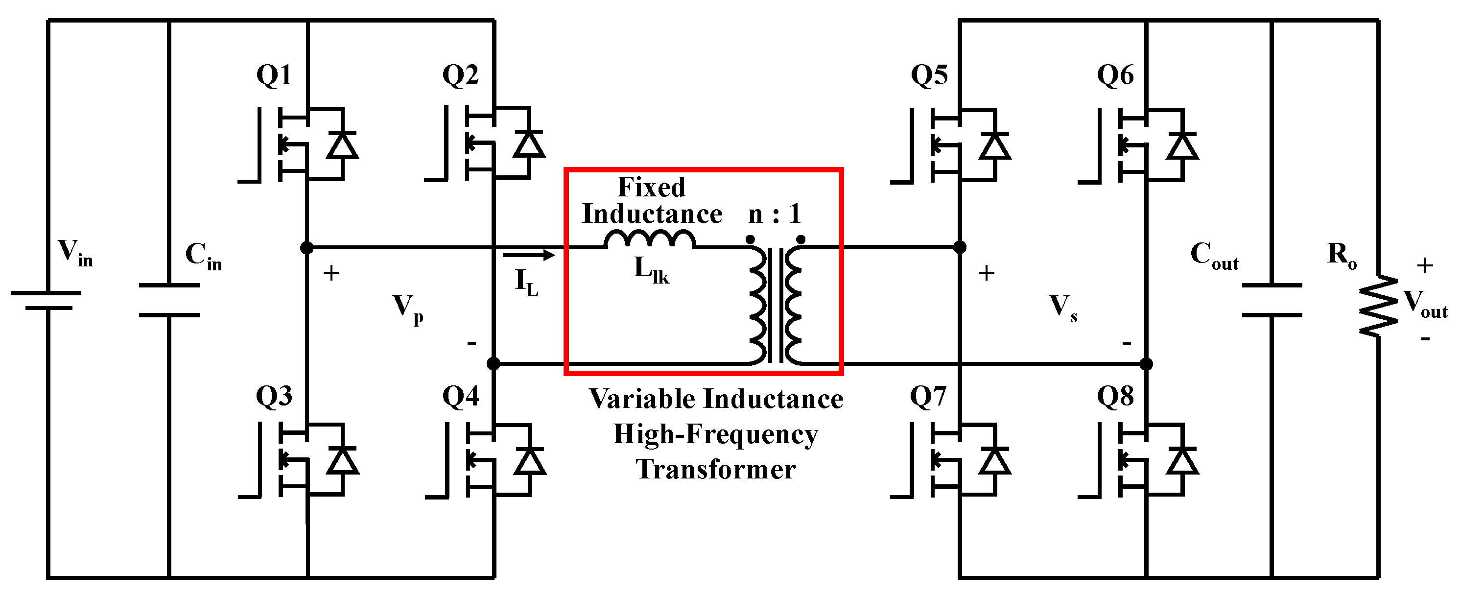
2. Proposed Variable Inductance Transformer
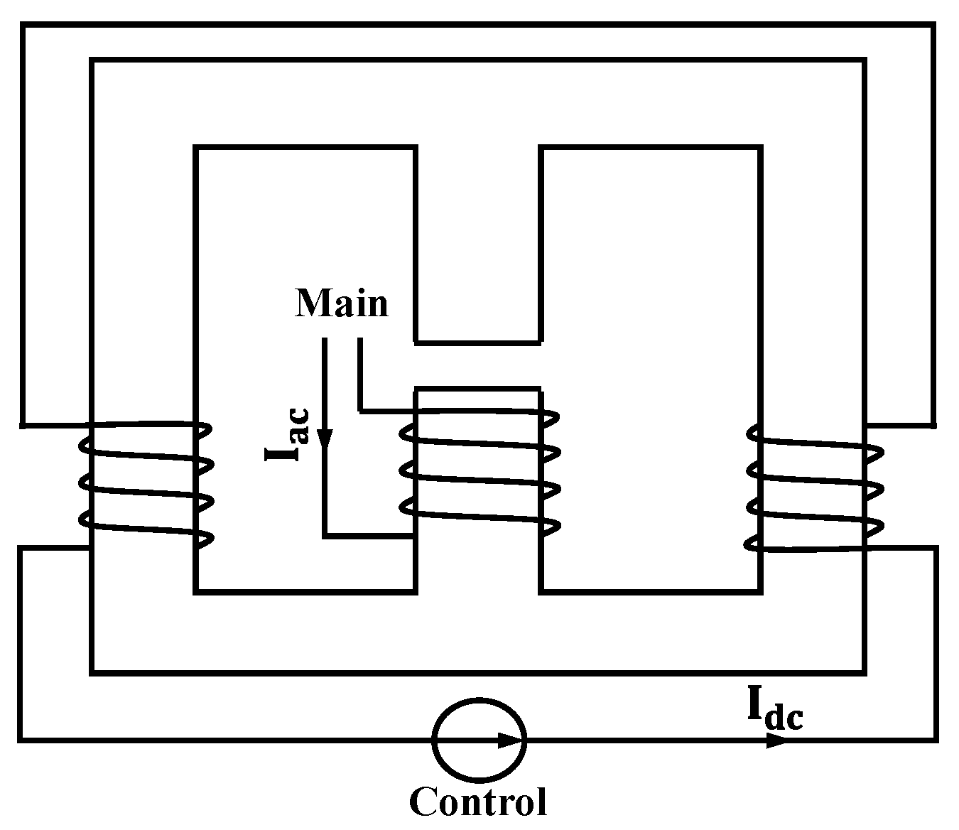
2.1. Conventional Variable Inductance Method
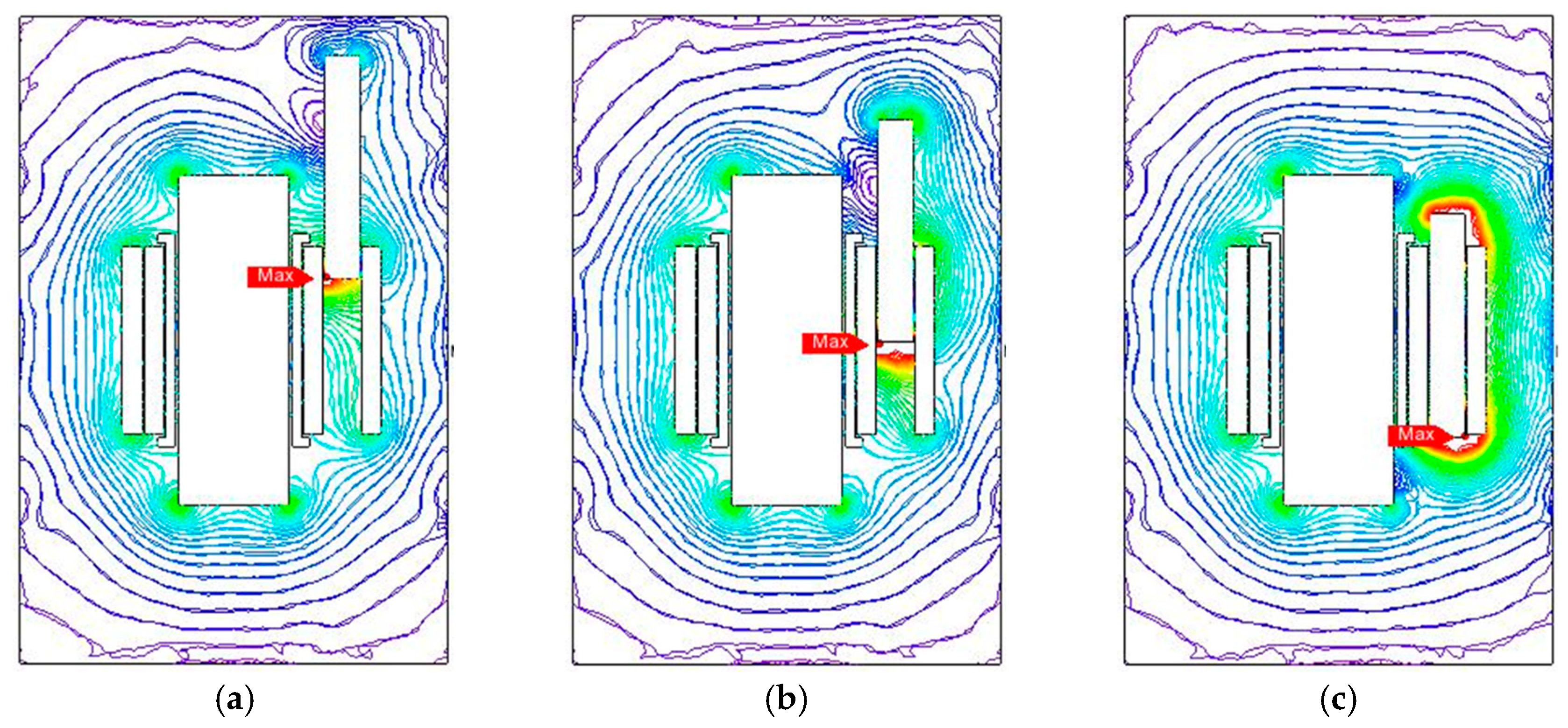
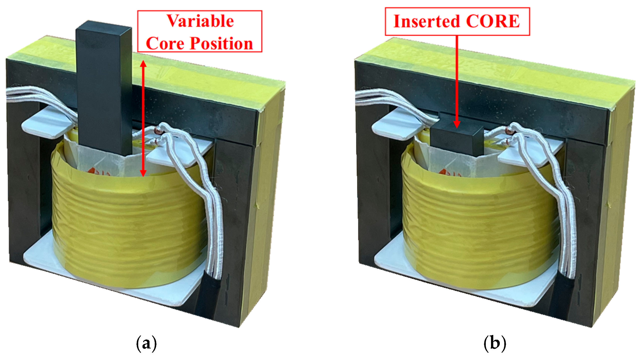
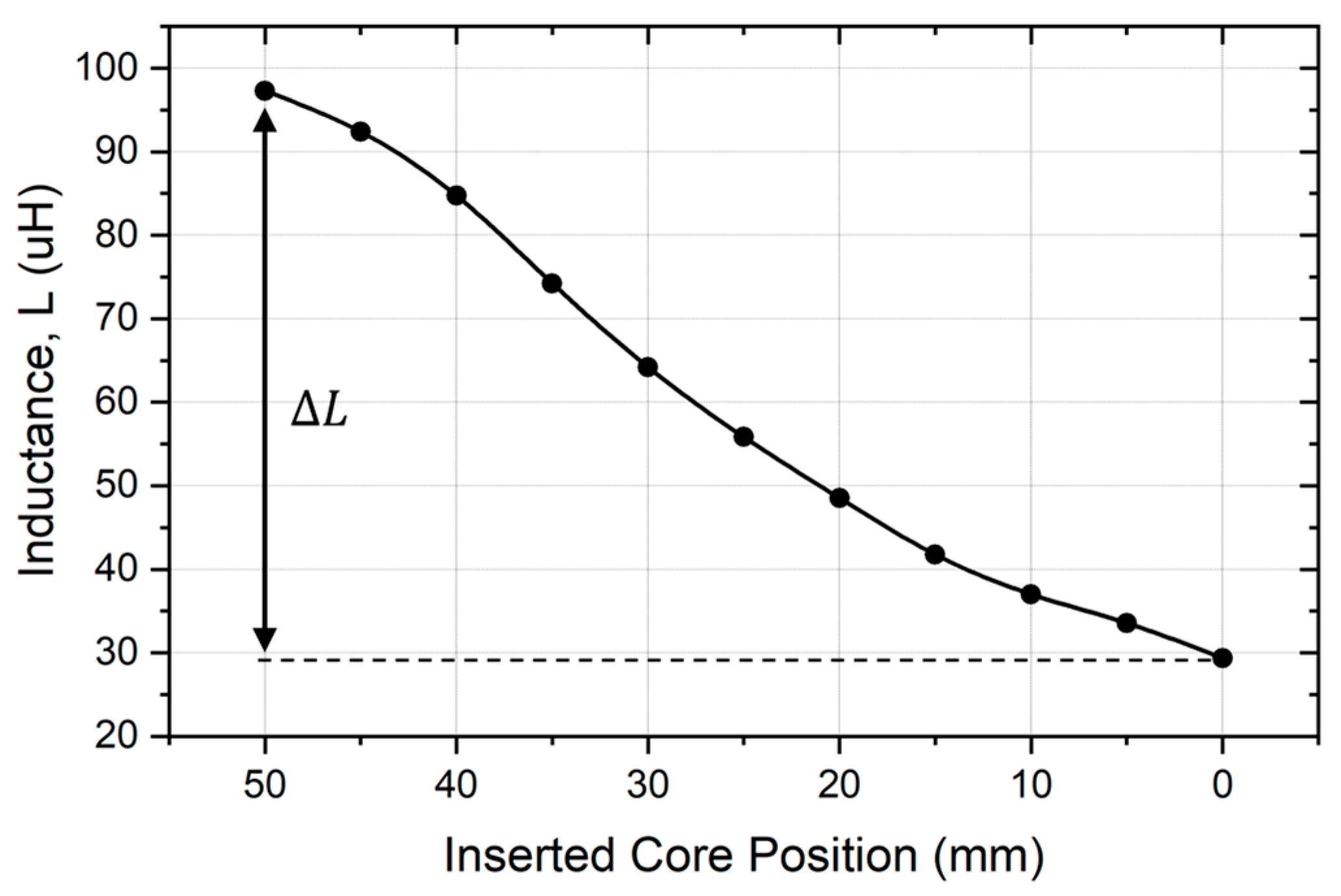
2.2. Proposed High-Frequency Transformer with Variable Inductance
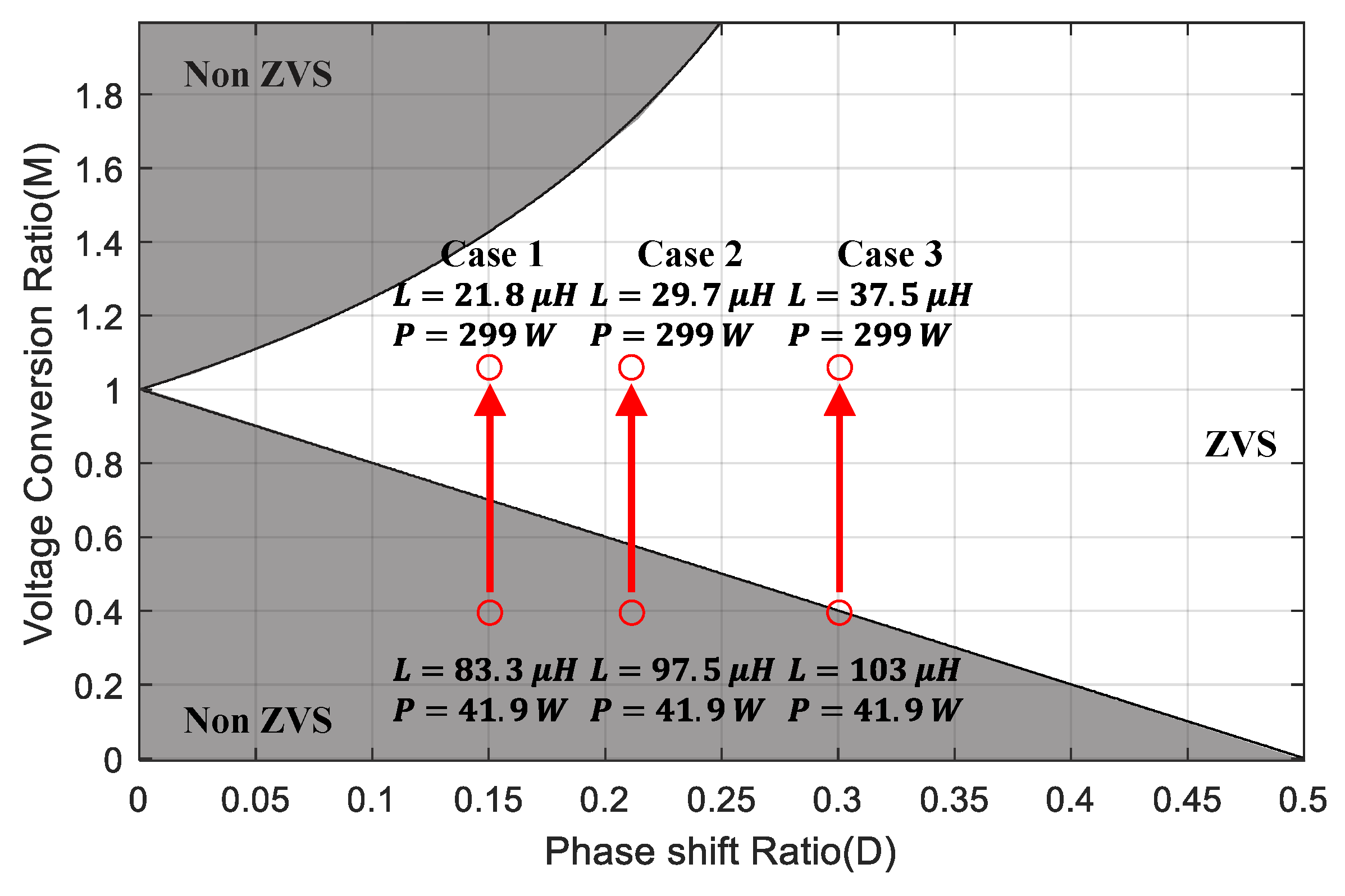
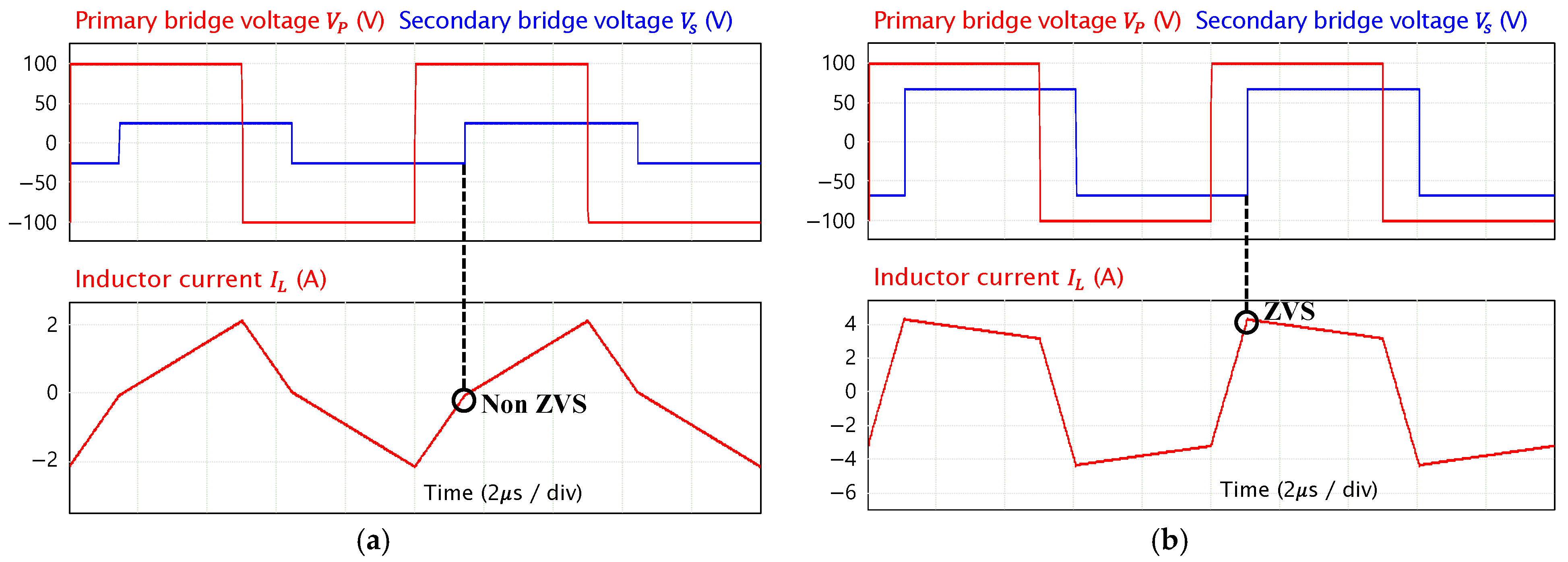
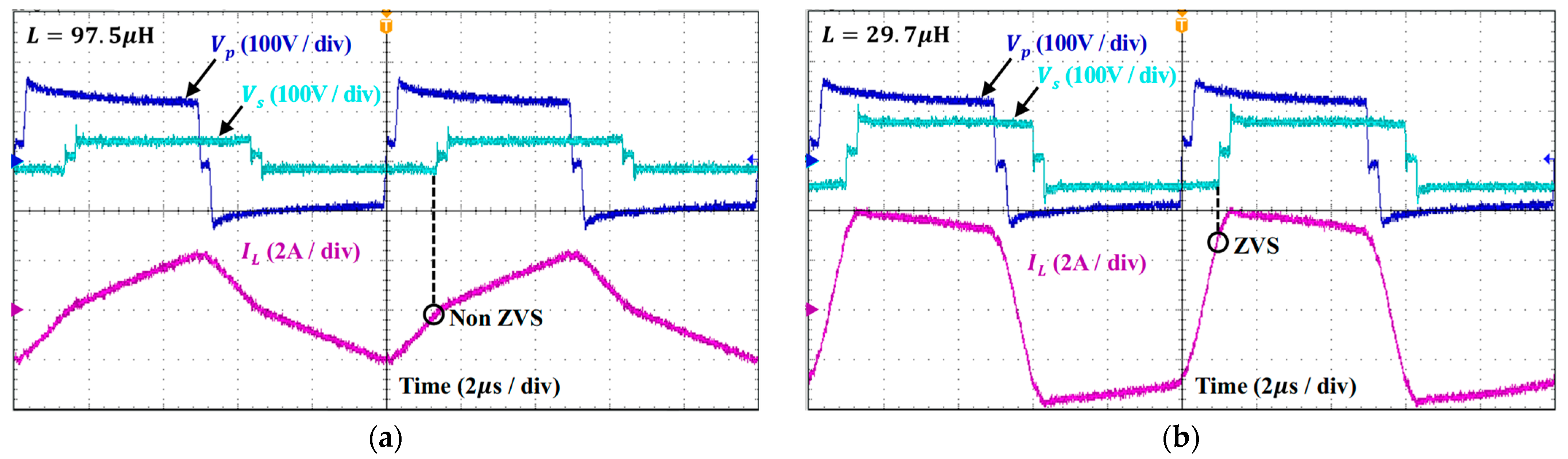
2.3. Zero-Voltage Switching Operation of DAB Converter
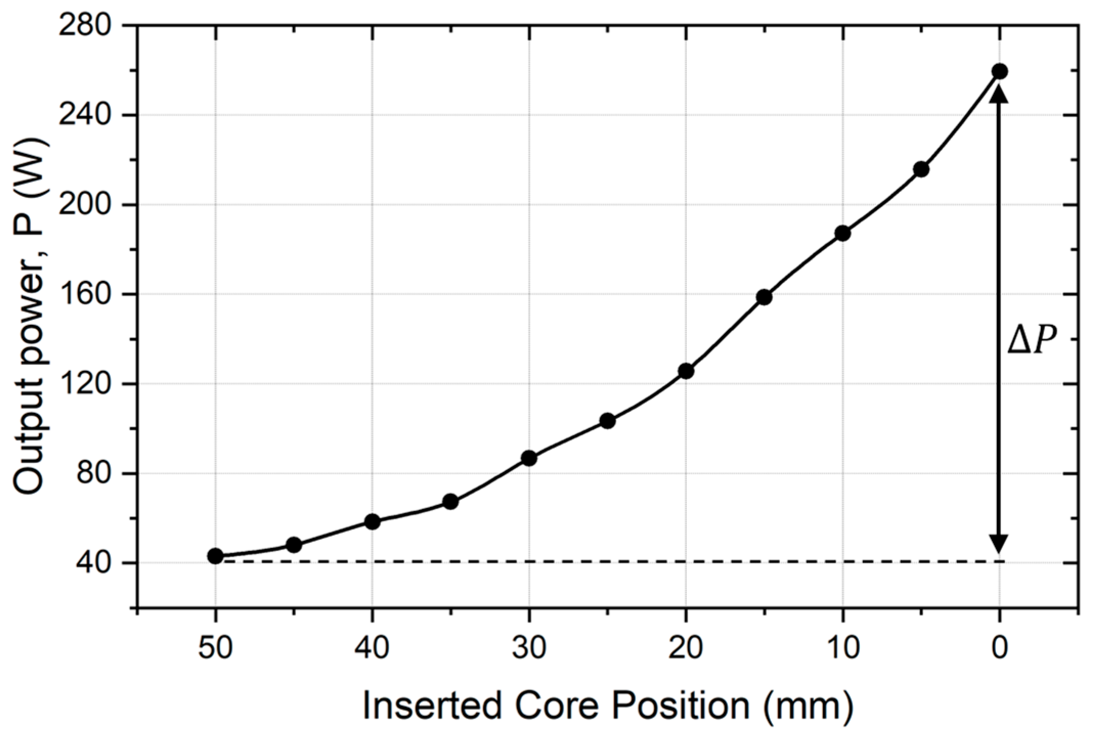
3. Simulation and Experimental Results
4. Conclusions
Author Contributions
Funding
Data Availability Statement
Conflicts of Interest
References
- Zhao, T.; Wang, G.; Bhattacharya, S.; Huang, A.Q. Voltage and Power Balance Control for a Cascaded H-Bridge Converter-Based Solid-State Transformer. IEEE Trans. Power Electron. 2013, 28, 1523–1532. [Google Scholar] [CrossRef]
- Parihar, K.S.; Pathak, M.K. Dual Mode Control Scheme for DAB Based Solid-State Transformer. IEEE Trans. Power Electron. 2024, 39, 3144–3155. [Google Scholar] [CrossRef]
- Lee, E.S.; Park, J.H.; Kim, M.Y.; Lee, J.S. High Efficiency Integrated Transformer Design in DAB Converters for Solid-State Transformers. IEEE Trans. Veh. Technol. 2022, 71, 7147–7160. [Google Scholar] [CrossRef]
- Becerra-Nuñez, G.; Castillo-Atoche, A.; Vazquez-Castillo, J.; Datta, A.; Quijano-Cetina, R.G.; Peña-Alzola, R.; Carrasco-Alvarez, R.; Osorio-De-La-Rosa, E. An FPGA Kalman-MPPT Implementation Adapted in SST-Based Dual Active Bridge Converters for DC Microgrids Systems. IEEE Access 2020, 8, 202946–202957. [Google Scholar] [CrossRef]
- de Doncker, R.W.; Divan, D.M.; Kheraluwala, M.H. A three-phase soft-switched high-power-density dc/dc converter for high-power applications. IEEE Trans. Ind. Appl. 1991, 27, 63–73. [Google Scholar] [CrossRef]
- Ataullah, H.; Iqbal, T.; Khalil, I.U.; Ali, U.; Blazek, V.; Prokop, L.; Ullah, N. Analysis of the Dual Active Bridge-Based DC-DC Converter Topologies, High-Frequency Transformer, and Control Techniques. Energies 2022, 15, 8944. [Google Scholar] [CrossRef]
- Turzyński, M.; Bachman, S.; Jasiński, M.; Piasecki, S.; Ryłko, M.; Chiu, H.-J.; Kuo, S.-H.; Chang, Y.-C. Analytical Estimation of Power Losses in a Dual Active Bridge Converter Controlled with a Single-Phase Shift Switching Scheme. Energies 2022, 15, 8262. [Google Scholar] [CrossRef]
- Khanzadeh, B.; Thiringer, T.; Kharezy, M. Multilevel Dual Active Bridge Leakage Inductance Selection for Various DC-Link Voltage Spans. Energies 2023, 16, 859. [Google Scholar] [CrossRef]
- Fan, H.; Li, H. High-frequency transformer isolated bidirectional DC–DC converter modules with high efficiency over wide load range for 20 kVA solid-state transformer. IEEE Trans. Power Electron. 2011, 26, 3599–3608. [Google Scholar] [CrossRef]
- Li, J.; Luo, Q.; Mou, D.; Wei, Y.; Sun, P.; Du, X. A Hybrid Five-Variable Modulation Scheme for Dual-Active-Bridge Converter With Minimal RMS Current. IEEE Trans. Ind. Electron. 2022, 69, 336–346. [Google Scholar] [CrossRef]
- Shi, H.; Wen, H.; Chen, J.; Hu, Y.; Jiang, L.; Chen, G.; Ma, J. Minimum-Backflow-Power Scheme of DAB-Based Solid-State Transformer with Extended-Phase-Shift Control. IEEE Trans. Ind. Appl. 2018, 54, 3483–3496. [Google Scholar] [CrossRef]
- Yazdani, F.; Zolghadri, M. Design of dual active bridge isolated bi-directional DC converter based on current stress optimization. In Proceedings of the 2017 8th Power Electronics, Drive Systems & Technologies Conference (PEDSTC), Mashhad, Iran, 14–16 February 2017. [Google Scholar]
- Perdigão, M.S.; Menke, M.; Seidel, A.R.; Pinto, R.A.; Alonso, J.M. A review on variable inductors and variable transformers: Applications to lighting drivers. In Proceedings of the 2014 IEEE Industry Application Society Annual Meeting, Vancouver, BC, Canada, 5–9 October 2014. [Google Scholar]
- Saeed, S.; Garcia, J.; Georgious, R. Dual-Active-Bridge Isolated DC–DC Converter with Variable Inductor for Wide Load Range Operation. IEEE Trans. Power Electron. 2021, 36, 8028–8043. [Google Scholar] [CrossRef]
- Saeed, S.; Georgious, R.; Garcia, J. Modeling of Magnetic Elements Including Losses—Application to Variable Inductor. Energies 2020, 13, 1865. [Google Scholar] [CrossRef]
- Jo, C.-H.; Kim, D.-H. A Novel Integrated OBC and LDC System with Improved Cross-Regulation Performance for Electric Vehicles. IEEE Trans. Ind. Electron. 2025, 72, 1452–1465. [Google Scholar] [CrossRef]
- Choi, D.; Lee, M.; Kim, T.; Kim, J.-S.; Moon, G.-W. Offset Current Modulation Technique for Wide ZVS Range in Dual Active Bridge (DAB) DC-DC Converter. IEEE Trans. Ind. Electron. 2024, 71, 8741–8751. [Google Scholar] [CrossRef]
- Buitrago, C.S.; Cobaleda, D.B.; Martinez, W. Dual Active Bridge Converter With Variable Transformer for Wide Voltage and Wide Load Range Operation. in IEEE Access 2023, 11, 90980–90998. [Google Scholar] [CrossRef]
- Choi, C.-W.; So, J.-H.; Ko, J.-S.; Kim, D.-K. Study on High-Frequency Transformer with Variable Inductance for Extending the Maximum Power Level of DAB Converter. In Proceedings of the 2024 IEEE 21st Biennial Conference on Electromagnetic Field Computation (CEFC), Jeju, Republic of Korea, 2–5 June 2024; pp. 1–2. [Google Scholar]
- Scirè, D.; Lullo, G.; Vitale, G. Assessment of the Current for a Non-Linear Power Inductor Including Temperature in DC-DC Converters. Electronics 2023, 12, 579. [Google Scholar] [CrossRef]
- Scirè, D.; Vitale, G.; Ventimiglia, M.; Lullo, G. Non-Linear Inductors Characterization in Real Operating Conditions for Power Density Optimization in SMPS. Energies 2021, 14, 3924. [Google Scholar] [CrossRef]
- Mi, C.; Bai, H.; Wang, C.; Gargies, S. Operation, design and control of dual H-bridge-based isolated bidirectional DC-DC converter. IET Power Electron. 2008, 1, 507–517. [Google Scholar] [CrossRef]
- Rodriguez, A.; Vazquez, A.; Lamar, D.G.; Hernando, M.M.; Sebastian, J. Different purpose design strategies and techniques to improve the performance of a dual active bridge with phase-shift control. IEEE Trans. Power Electron. 2015, 30, 790–804. [Google Scholar] [CrossRef]


| Core Depth | Parameter | Joule Loss | Iron Loss | Hysteresis Loss | Total Loss |
|---|---|---|---|---|---|
| Transformer Core | |||||
| Inserted Core | |||||
| Transformer Core | |||||
| Inserted Core | |||||
| Transformer Core | |||||
| Inserted Core | |||||
| Transformer Core | |||||
| Inserted Core | |||||
| Transformer Core | |||||
| Inserted Core | |||||
| Transformer Core | |||||
| Inserted Core |
| Parameter | Value |
|---|---|
| Transformer Core Type | ) |
| Transformer Core Magnetic Material | PM11 |
| Inserted Core Type | ) |
| Inserted Core Magnetic Material | PM11 |
| Winding Type | Litz wire |
| Primary (1st) Winding Turns | 29 |
| Secondary (2nd) Winding Turns | 18 |
| Turns Ratio | 1.61 (29:18) |
| Parameter | Unit | Value |
|---|---|---|
| Input Voltage | V | 100 |
| Output Voltage | V | 40~62.5 |
| Switching Frequency | kHz | 100 |
| Leakage Inductance | μH | 29.7~97.5 |
| Dead Time | ns | 380 |
| Load Resistance | Ω | 25 |
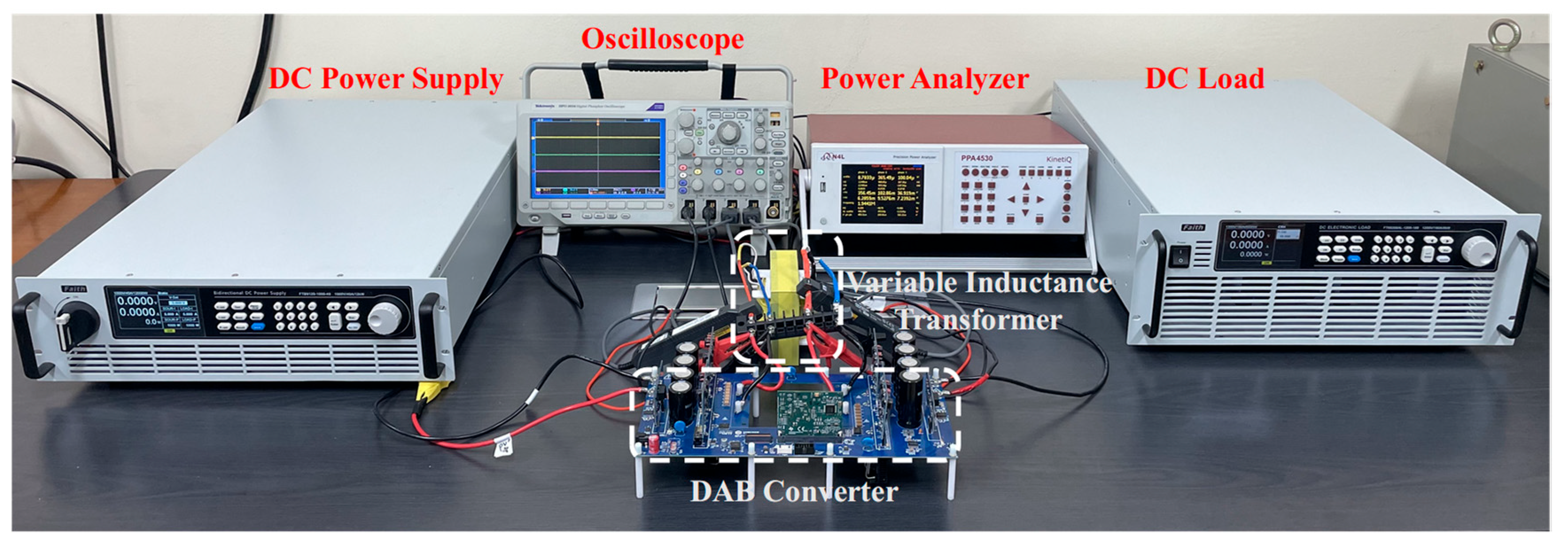
| Equipment Name | Manufacturer | Model Number |
|---|---|---|
| DC Power Supply | Faith (Shenzhen, China) | FTB9120-1000-40 |
| Oscilloscope | Tektronix (Beaverton, OR, USA) | DPO3034 |
| Power Analyzer | N4L (Leicester, UK) | PPA4530 |
| DC Load | Faith (Shenzhen, China) | FT68206AL-1200-180 |
Disclaimer/Publisher’s Note: The statements, opinions and data contained in all publications are solely those of the individual author(s) and contributor(s) and not of MDPI and/or the editor(s). MDPI and/or the editor(s) disclaim responsibility for any injury to people or property resulting from any ideas, methods, instructions or products referred to in the content. |
© 2025 by the authors. Licensee MDPI, Basel, Switzerland. This article is an open access article distributed under the terms and conditions of the Creative Commons Attribution (CC BY) license (https://creativecommons.org/licenses/by/4.0/).
Share and Cite
Choi, C.-W.; Ko, J.-S.; Yoon, K.-Y.; Park, Y.-U.; Kang, Y.-S.; Kim, D.-K. A Novel Structure of Variable Inductance High-Frequency Transformer for Power Level Enhancement in Dual-Active-Bridge Converters. Energies 2025, 18, 1043. https://doi.org/10.3390/en18051043
Choi C-W, Ko J-S, Yoon K-Y, Park Y-U, Kang Y-S, Kim D-K. A Novel Structure of Variable Inductance High-Frequency Transformer for Power Level Enhancement in Dual-Active-Bridge Converters. Energies. 2025; 18(5):1043. https://doi.org/10.3390/en18051043
Chicago/Turabian StyleChoi, Cheol-Woong, Jae-Sub Ko, Keun-Yong Yoon, Yong-Un Park, Yun-Soo Kang, and Dae-Kyong Kim. 2025. "A Novel Structure of Variable Inductance High-Frequency Transformer for Power Level Enhancement in Dual-Active-Bridge Converters" Energies 18, no. 5: 1043. https://doi.org/10.3390/en18051043
APA StyleChoi, C.-W., Ko, J.-S., Yoon, K.-Y., Park, Y.-U., Kang, Y.-S., & Kim, D.-K. (2025). A Novel Structure of Variable Inductance High-Frequency Transformer for Power Level Enhancement in Dual-Active-Bridge Converters. Energies, 18(5), 1043. https://doi.org/10.3390/en18051043