1. Introduction
Modular and multilevel converters are extensively used in high-power applications, such as high-voltage direct current (HVDC) transmission systems and medium-voltage drives. These converters offer significant advantages, including lower switching losses and improved power quality. By utilizing low-power rating switches, modular and multilevel converters facilitate the development of high-power rating systems while minimizing voltage stress (dv/dt) and challenges related to electromagnetic interference. They also help reduce total harmonic distortion and enable a lower switching frequency, further decreasing voltage stress levels and switching losses. One of the most critical features of modular converters is their ability to operate under fault conditions, although their power rating may be reduced if they are unable to tolerate these faults [
1,
2,
3,
4,
5,
6,
7,
8,
9,
10,
11,
12,
13,
14,
15]. Beyond the high-power DC-DC focus of this work, modular converter principles are also being advanced for complex multi-source/load systems, such as in AC nanogrids, where novel modulation strategies like dynamic weighted-selection are being developed to manage power flow among multiple renewable sources and loads [
16]. Since most modular and multilevel converters are designed for high-power applications, it is essential to implement fault-tolerant techniques to address any faults that may occur during normal operation [
12,
13,
14,
15]. Research on power converter faults primarily focuses on capacitors and switching transistors, which account for a significant portion of failures. Common fault types include open circuits, short circuits, and component degradation. To address these issues, various fault detection and diagnosis methods have been developed, such as sliding mode observers, support vector machines, and higher-order harmonic analysis. Additionally, statistical techniques are employed to analyze component behavior and identify anomalies. These studies underscore the importance of effective fault detection and diagnosis in enhancing the reliability of power converters [
4,
12,
17]. The study referenced in [
18] utilized the duty–cycle ratio, input and output voltages, and inductor current to detect MOSFET degradation. In [
19], electrical measurements were combined with an adaptive model and machine learning algorithms to monitor the on-state resistance of power gallium nitride (GaN) transistors. Additionally, the research in [
5] employed available electrical measurements of the converter alongside machine leaning algorithms to identify MOSFET degradation. However, measurements of the inputs and outputs of the converter alone are insufficient to determine its health. It is essential to include link converter measurements to provide a complete picture of the converter’s condition. A major issue of how to restore the power converter to a healthy state after faults occur remains, highlighting the importance of knowing how to tolerate and manage faults in power converters. Fault-tolerant design for high-voltage modular DC-DC converters faces several challenges and limitations. Key challenges include the complexity of designing systems that can manage various faults without degrading performance and developing reliable, real-time fault detection and isolation techniques. Achieving a balance between component reliability and redundancy while maintaining cost, size, and efficiency is critical. The integration of modular designs into existing systems, scalability, and flexibility are also significant challenges [
20,
21,
22,
23].
Table 1 summarizes fault-tolerant solutions for DC open-circuit and short-circuit faults in the literature. The fault-tolerant solutions for DC open-circuit and short-circuit faults in Multilevel Modular Converters (MMCs) exhibit a clear trade-off between hardware complexity and system resilience. For open-circuit faults, software-based strategies (e.g., PWM reference adjustments) require no additional switches [
24,
25], while hardware redundancy (e.g., spare submodules or MMCCC integration) introduces 2–4 extra switches per redundant SM [
26,
27]. In contrast, short-circuit fault mitigation demands more aggressive hardware modifications: full-bridge SMs (4 switches/SM), clamp-diode SMs (5 switches/SM), or cross-connected SMs (6 switches/SM) double or triple the switch count compared to standard half-bridge SMs, alongside external breaker solutions (2–6 switches per branch). Hybrid approaches (e.g., partial FBSM adoption) and cold/spinning reserve configurations strike a balance between fault tolerance and cost, though at the expense of increased control complexity and losses. These findings underscore the need for application-specific optimization to align reliability goals with economic and operational constraints [
28,
29]. Adding more switches improves the fault tolerance but raises cost, losses, and control complexity. Hence, hybrid solutions that could balance performance and cost are required. Limitations include the high cost of fault-tolerant features, technological constraints such as sensor precision and semiconductor durability, and the lack of standardization, which can lead to compatibility issues. Testing and validation are complex due to the difficulty in simulating all fault conditions. Additionally, advanced control algorithms and communication protocols can introduce overhead and latency, impacting system performance. Addressing these issues requires ongoing innovation to ensure robust and cost-effective designs that enhance system reliability and longevity [
30,
31,
32,
33,
34,
35,
36,
37]. The author in [
38,
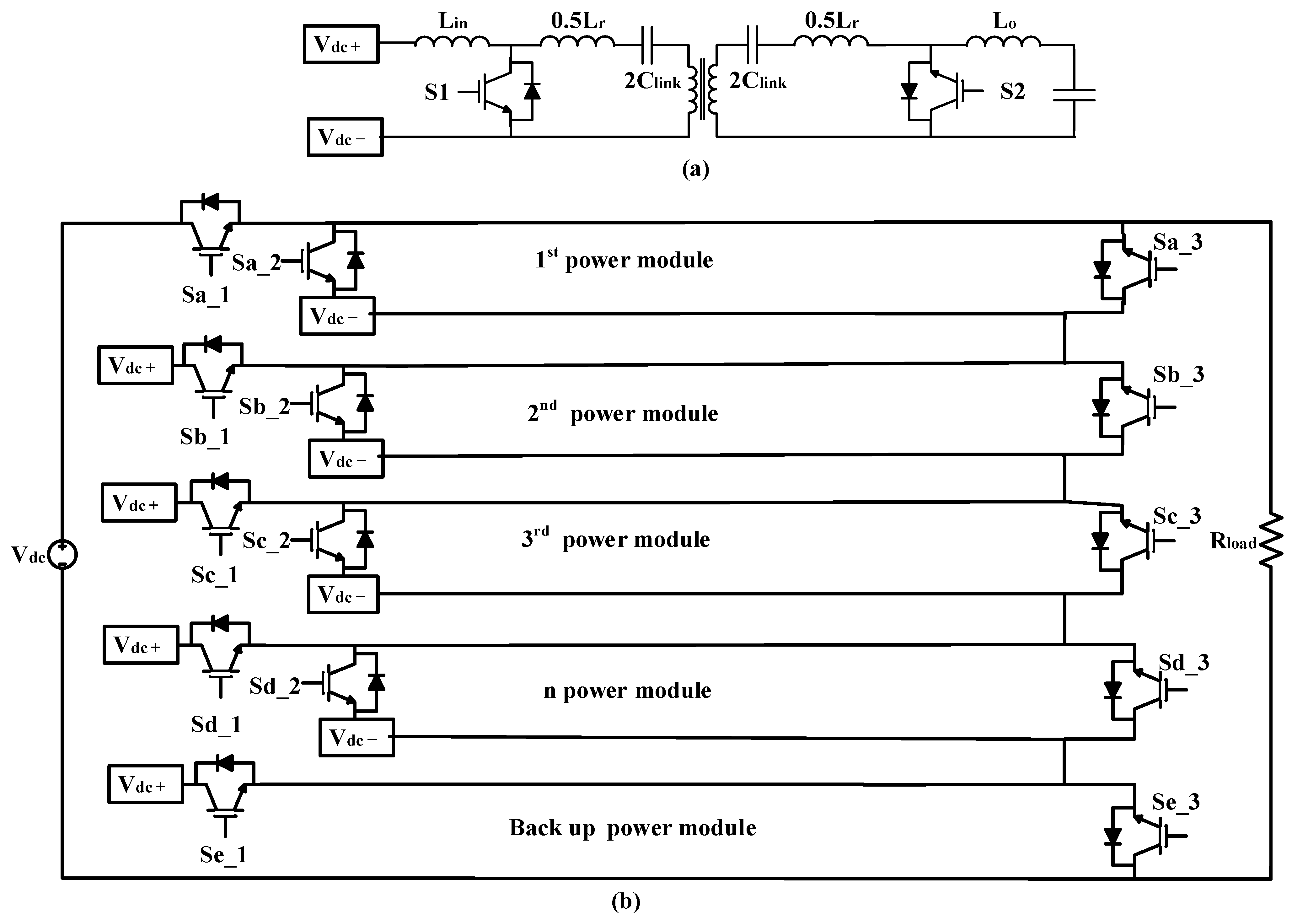
39] introduces a modular DC-DC converter for high-power applications, designed to use two small film capacitors in each power module for power transfer from the source to the load, as shown in
Figure 1a. The design eliminates the need for large electrolytic capacitors, which are known for high failure rates and temperature sensitivity, thereby reducing potential faults.
Each module operates as an isolated converter with a high-frequency transformer, leveraging its leakage inductance for zero current turn-off and soft turn-on, which results in low conduction losses. These modular converters can be configured in series or parallel to achieve voltage or current sharing in high-power scenarios. The focus of the paper is on an input-parallel output-series (IPOS) configuration that enhances voltage blocking capability and accommodates high input currents.
A novel fault-tolerant method tailored for this modular converter architecture is presented in [
38,
39], covering its operation, design, and analysis as displayed in
Figure 1b. The effectiveness of the approach is validated through simulations. Notably, the proposed method is applicable to a wide range of modular converters used in high-power applications. The advanced control technique can transform a faulty system into a fully operational one without requiring human intervention. An example demonstrates the algorithm in action, applied to the converter topology outlined in [
38,
39]. Representing a significant advancement in power electronics, the control-driven fault-tolerant strategy enhances reliability, efficiency, and durability of modular DC-DC converters—qualities essential for critical applications such as renewable energy systems, electric vehicles, and distributed power generation. The main contributions of the paper include the following:
A novel framework integrating real-time fault detection (open-circuit, short-circuit) and autonomous reconfiguration via advanced control algorithms, eliminating the need for system shutdown.
A hybrid approach combining redundant power modules, reconfigurable interconnections, and optimized semiconductor switches to isolate faults while maintaining continuous operation.
A scalable topology validated through simulations, adaptable to diverse high-power applications (e.g., HVDC, renewable energy).
2. The Principle of Operation
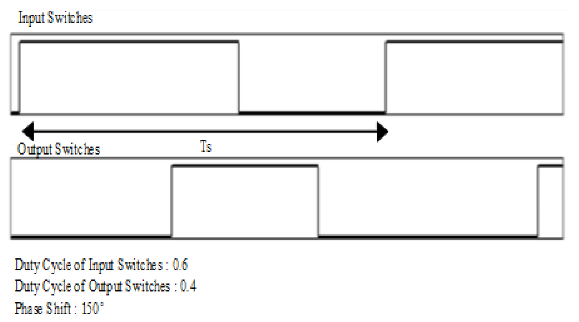
The operation of all modules follows the same principle: the input-side switches of all power modules are synchronized, turning on and off simultaneously. Likewise, the output-side switches of each power module are activated and deactivated at the same time, as illustrated in
Figure 1b. The corresponding duty cycles for both the input and output switches are shown in
Figure 2.
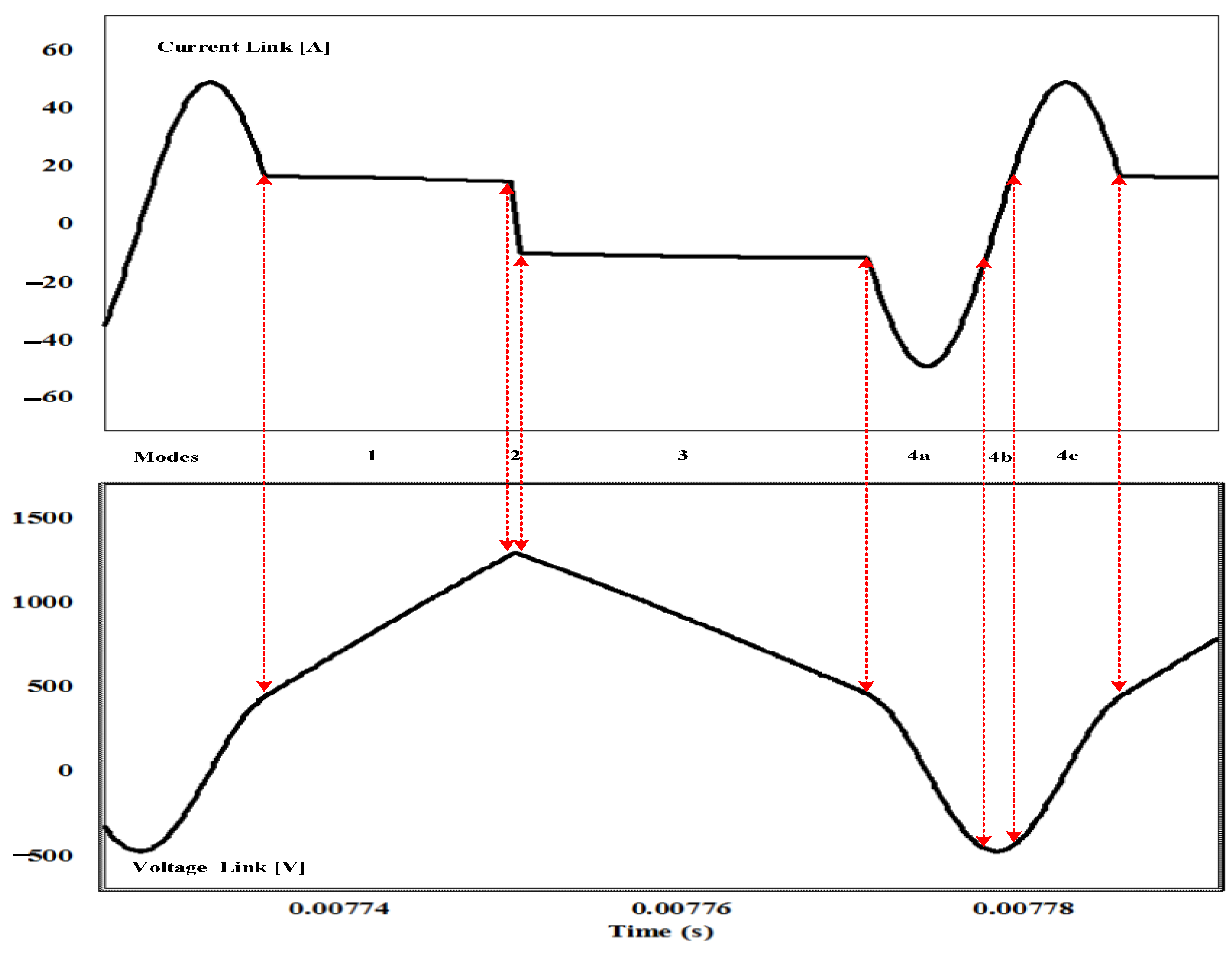
The converter operates in four different modes. In Mode 1, called the charging mode, both switches are off, and the output diode allows current to pass from the input to the output, which charges the link capacitors and results in a linear increase in link voltage. Mode 2 is a resonant mode where both the input switch and output diode conduct, forming a resonant circuit with the link components. During this phase, the input-switch current rises while the output-diode current falls, eventually causing the link current to reverse direction. Mode 3, the discharging mode, involves link current flowing from the output back to the input, discharging the link capacitors and reducing the link voltage. It is crucial to stop this mode before the capacitors are fully discharged. Mode 4 is a more complex resonant mode consisting of three stages: first, both switches conduct, leading to a negative increase and subsequent decrease in the link current; next, the output switch turns off, allowing the link current to rise positively; finally, the input switch turns off, and the link current continues to rise until it matches the input current before starting to decrease.
The transition between modes is governed by the resonant parameters and switching timing. For instance, the resonant frequency in Mode 2 is critical for soft switching and is derived as follows:
where
and
are the link inductor and capacitor values, respectively. The chosen duty cycles
= 0.6,
= 0.4 optimize energy transfer while minimizing switching losses, validated by the following condition:
where
is the dead time and
is the switching period. The Transformer’s leakage inductance (
) is selected to ensure zero-current turn-off, calculated as follows:
The timing and behavior of these modes depend on the component values and the types of switches used. All modes of operations can be seen in
Figure 3 where
is the peak link current.
3. Design and Analysis
Equations (4) and (5) can be used to describe the behavior of the circuit during charge and discharge modes, assuming that the converter link capacitors operate at the boundary of continuous conduction mode and discontinuous conduction mode, and that the turn ratio of the transformer is 1:1.
where
are the average input and output voltages of each power module,
and
are the durations of charging and discharging modes,
is the switching frequency, and
is the total link peak voltage as displayed in
Figure 3. Hence, the peak voltage across each switch and diode of a power module will be equal to
.
If the turn ratio of the transformer is
, the number of required power modules N is the number of power modules,
Iin and
Iout are the input and output currents of the primary and secondary power modules as follows:
The V
in and V
o for each primary and secondary power module can be determined by Equations (12) and (13) as follows:
Hence, the value of the primary link capacitors will be affected by a as follows:
The value of the capacitor for each primary and secondary power module can be determined from Equation (15) when
as follows:
The peak voltage across the switches in primary and secondary side of the power module,
, can be obtained from this equation as follows:
The number of required power modules,
N, can be determined by (18) as follows:
The voltage stress across switches (
) scales with the turn ratio
a. For
a =1,
necessitating 1200 V-rated SiC MOSFETs for a 500 V input system. Current stress during faults is mitigated by the backup module’s activation time (<50 µs), ensuring safe operation within safe operation area limits. The design scales linearly with power: for N > 4 modules, the redundancy overhead decreases from 25% (N + 1) to 10% (N + 2), while maintaining <1.5% voltage dip. Conduction losses increase by 0.3% per redundant path, but total efficiency remains >98% due to ZCS. Given that all modules operate identically during both charging and discharging modes, adding a backup power module would enhance system reliability. This backup module, isolated from the main converter, could be deployed in the event of a fault. Additionally, input and output switches should be integrated into each power module to isolate faulty units and safely divert faulty current to the ground, as illustrated in
Figure 4. The fault-tolerant strategy can be described as follows:
The presented analysis and simulations utilize idealized components to clearly demonstrate the operational principles and fault-tolerant capability of the proposed converter. In a practical implementation, parasitic elements such as capacitor ESR, MOSFET and transformer losses (core and copper) would impact the overall efficiency and thermal profile. The conduction losses from ESR and would contribute to the overall power loss, slightly reducing the simulated efficiency. The resonant trajectories would experience damping due to these resistances, requiring minor adjustments to the timing to maintain soft switching. These effects are mitigated by the selection of high-performance components: low-ESR film capacitors, SiC MOSFETs with low and a transformer designed with Litz wire and a low-loss ferrite core to minimize magnetic losses at high frequency. A comprehensive thermo-electronic co-simulation including these parasitics is reserved for future work focused on prototype development and optimization.
In
Figure 4, the modular DC-DC converter introduced in [
38,
39] consists of four power modules. To enhance reliability, an additional power module is incorporated into the circuit to serve as a backup. Each power module is also equipped with two input-side switches and one output-side switch. In the event of a failure in any of the four original power modules, the backup module is activated, and the faulty module is isolated.
During normal, fault-free operation, the input-side switches Sa_1 to Sd_1 remain engaged to interconnect each power module, while the switches Sa_2 to Sd_2 on the input side and Sa_3 to Sd_3 on the output side remain off. In this state, the backup module is kept on standby by turning off Se_1 and keeping Se_3 on.
If a fault occurs in any power module, whether it is a short-circuit or open-circuit fault, the system can isolate the defective module. To achieve this, the respective input-side switch (Sa_1 to Sd_1) is turned off, and the corresponding switches Sa_2 (input) and Sa_3 (output) are turned on. For example, if the topmost power module fails, Sa_1 is turned off while Sa_3 is turned on to isolate the faulty module. Additionally, Sa_2 is turned on to safely discharge the faulty module’s energy to the ground. Simultaneously, the backup module is brought online by turning on Se_1 and turning off Se_3, allowing the system to continue normal operation.
To further optimize this fault-tolerant mechanism, advanced control including advanced control algorithms, is integrated into the process. These advanced control-driven algorithms continuously monitor the health of each power module, predict potential faults, and automate the switching process to ensure seamless operation and minimize downtime. The application of an advanced control algorithm is illustrated in
Figure 5. This intelligent advanced control approach enhances the system’s resilience and overall efficiency by ensuring the timely isolation of faulty modules and the smooth activation of backup power. The proposed advanced control algorithm begins by continuously collecting operational data (voltages, currents) from the modular converter, which is analyzed in real time to detect anomalies like voltage fluctuations or current spikes. When a fault is suspected, the system immediately determines whether it is an open-circuit or short-circuit fault based on predefined thresholds (e.g., zero current with an active gate signal for open-circuit, or near-zero voltage with current surge for short-circuit). Once a fault is confirmed, the algorithm isolates the faulty module by disabling its input switch, activating a discharge path to safely release stored energy, and connecting the output isolation switch. Simultaneously, a backup module is seamlessly activated to restore full system operation within 500 μs, ensuring uninterrupted power delivery. Post-recovery, the system validates output stability before resuming normal operation. This deterministic, rule-based approach ensures fast, reliable fault mitigation through advanced control, as demonstrated in the simulation results (
Figure 6,
Figure 7,
Figure 8,
Figure 9,
Figure 10,
Figure 11,
Figure 12 and
Figure 13).
- (a)
Remark on Cybersecurity and FDI Attacks: The advanced control algorithm presented in this work is designed for resilience against physical component faults and internal electrical transients. Its efficacy is predicated on the integrity of the sensor data and control signals. The algorithm does not incorporate specific mechanisms to detect or mitigate stochastic False Data Injection (FDI) cyber-attacks, where an adversary maliciously alters sensor readings or command signals. In such a scenario, the trust-based logic of the fault detection could be deceived. Extending this framework to be robust against cyber-physical attacks represents an important direction for future research, potentially involving cryptographic signal authentication, model-based residual analysis, and cross-correlation with hardware-level fingerprints that are more difficult to spoof.
Figure 5.
Advanced control algorithm applied to the proposed configuration.
Figure 5.
Advanced control algorithm applied to the proposed configuration.
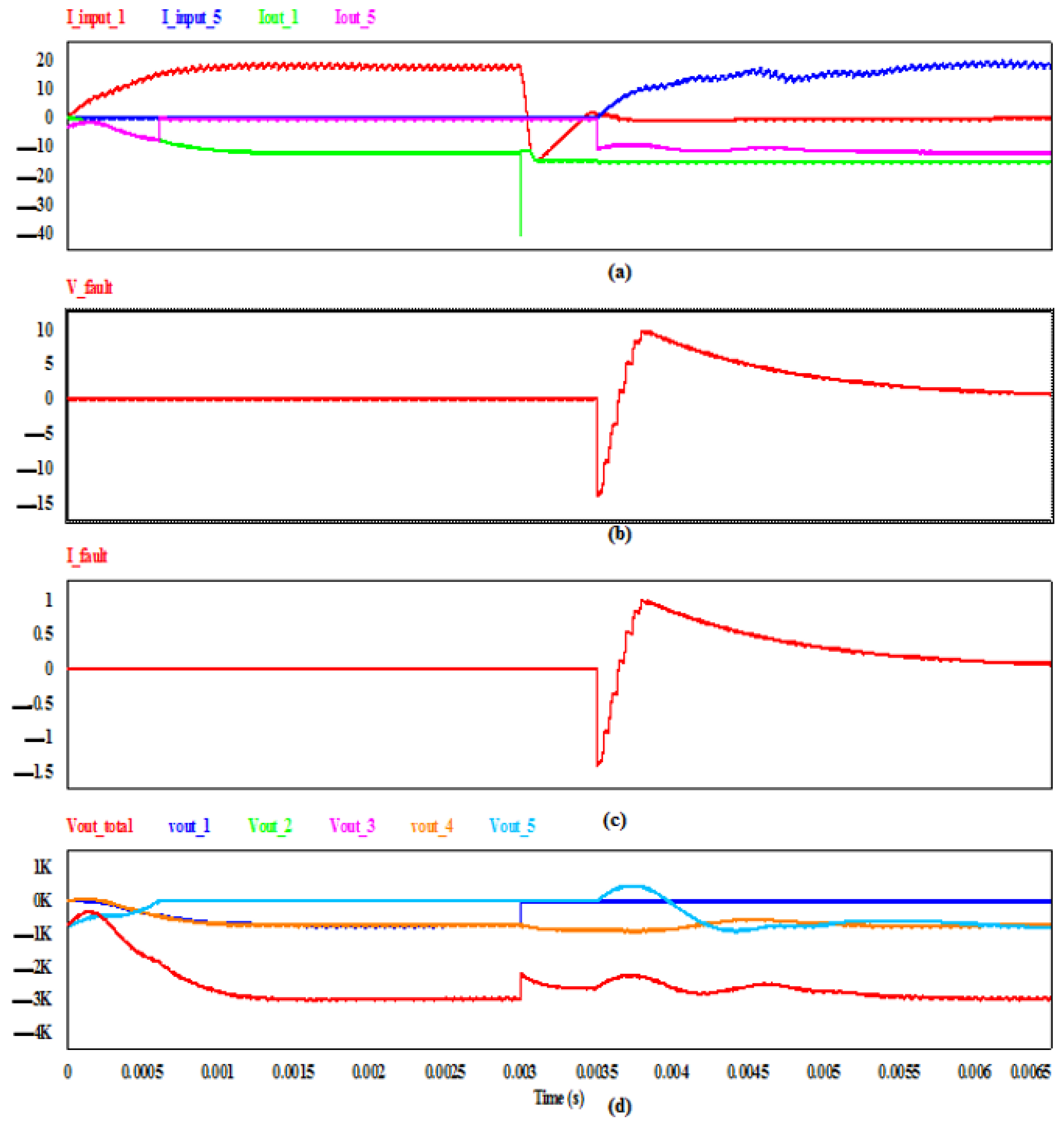
Figure 6.
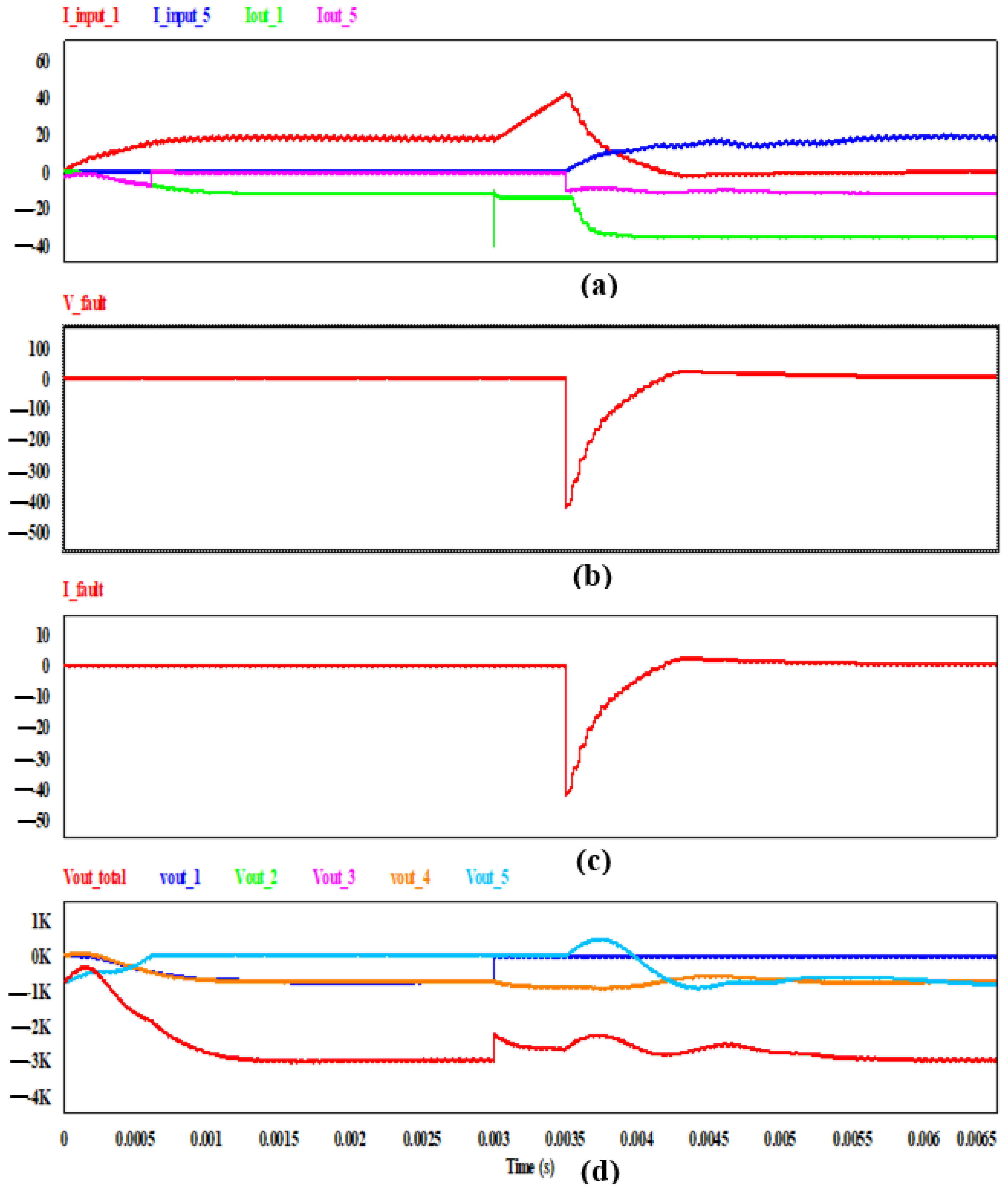
The behavior of the converter during healthy and faulty conditions for case 1: (a) input and output currents (b) the faulty voltage (c) the faulty current, and (d) output voltages and total output voltages.
Figure 6.
The behavior of the converter during healthy and faulty conditions for case 1: (a) input and output currents (b) the faulty voltage (c) the faulty current, and (d) output voltages and total output voltages.
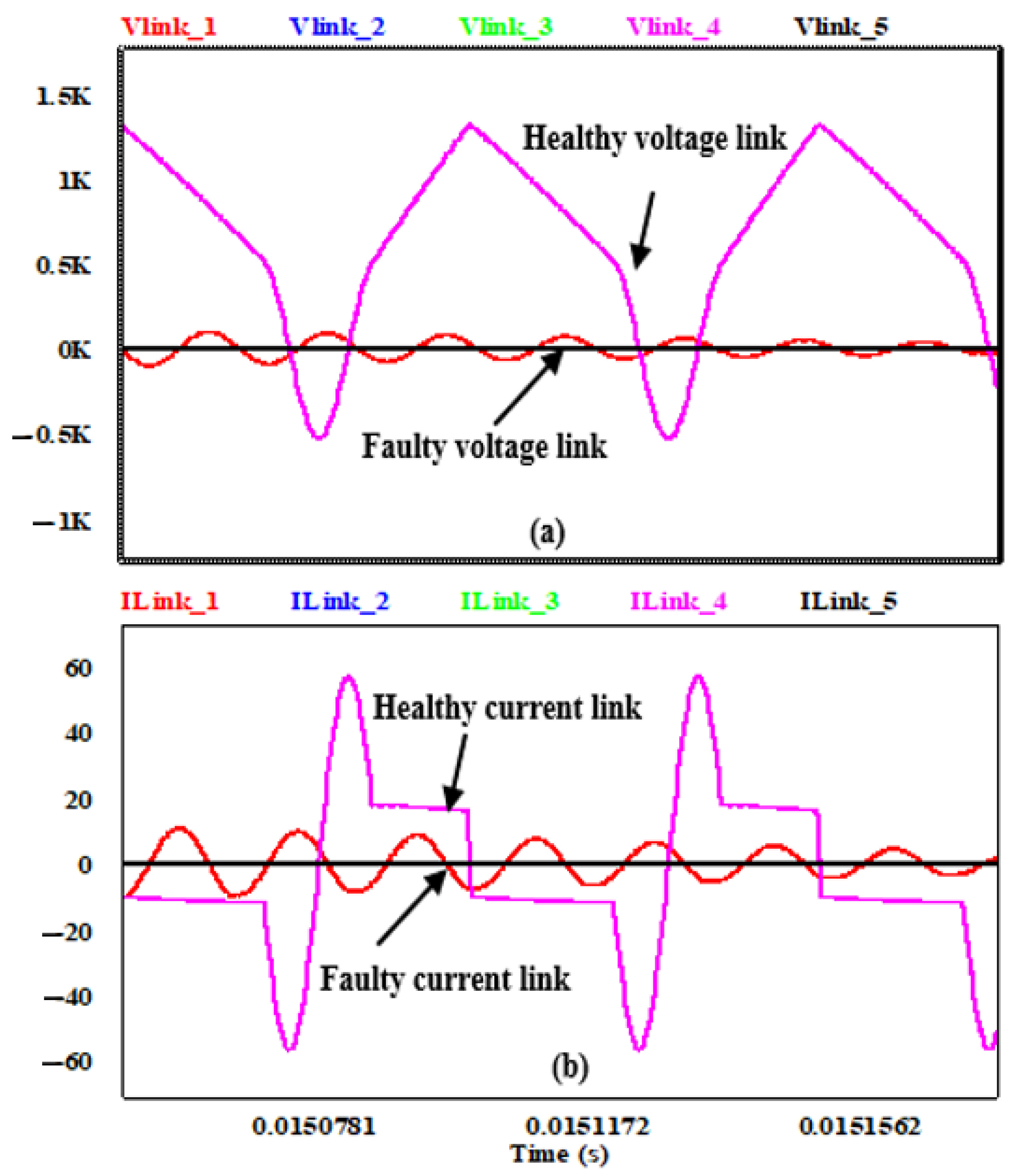
Figure 7.
The behavior of link voltages and currents during the fault at the faulty and healthy power modules: (a) Link Voltages and (b) Link Currents.
Figure 7.
The behavior of link voltages and currents during the fault at the faulty and healthy power modules: (a) Link Voltages and (b) Link Currents.
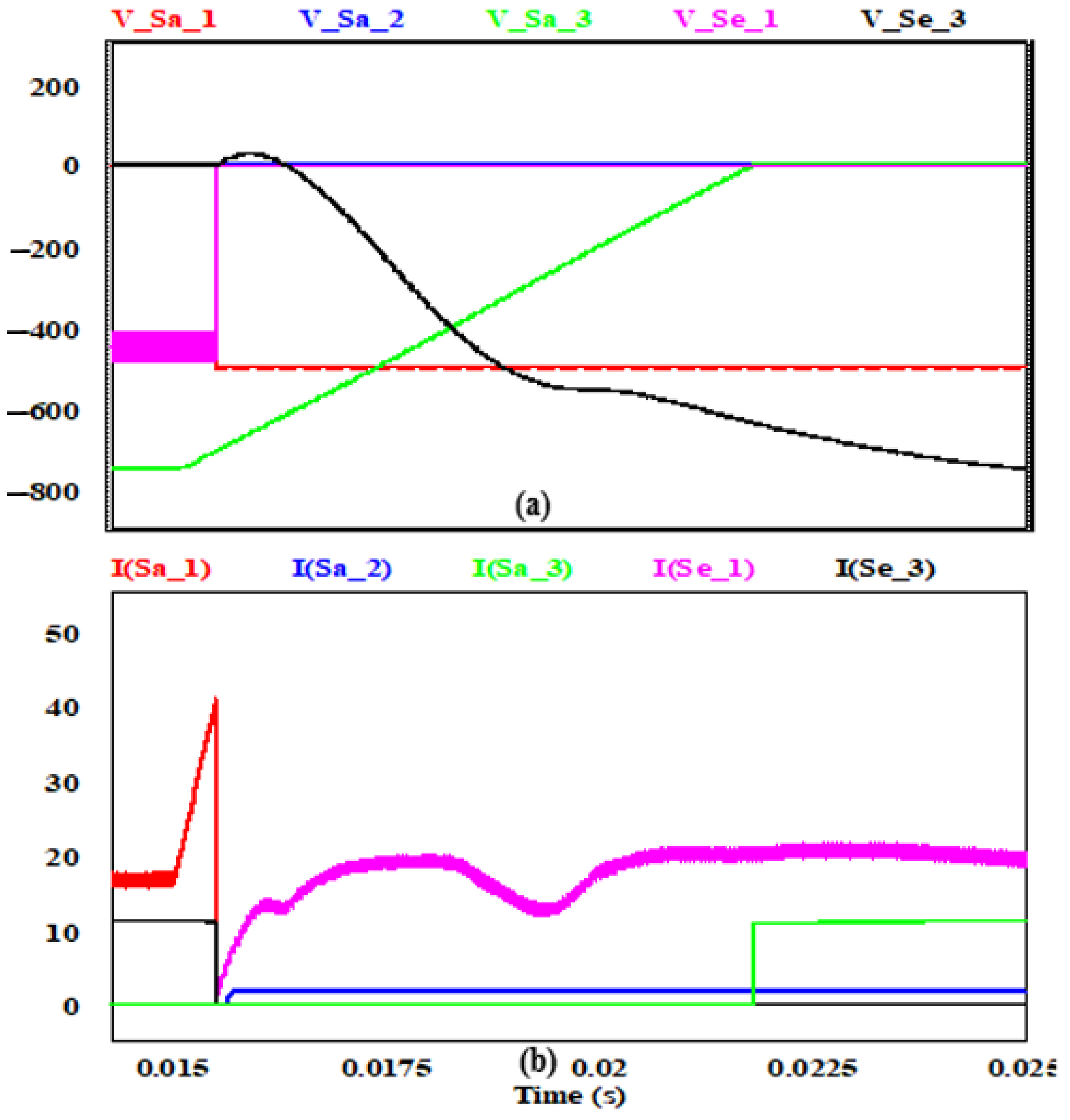
Figure 8.
Simulation results of the faulty and healthy power modulas, (
a) the voltage across Sa_1, Sa_2, Sa_3, Se_1, Se_3 switches in
Figure 4, (
b) the current flowing through the same switches in
Figure 4.
Figure 8.
Simulation results of the faulty and healthy power modulas, (
a) the voltage across Sa_1, Sa_2, Sa_3, Se_1, Se_3 switches in
Figure 4, (
b) the current flowing through the same switches in
Figure 4.
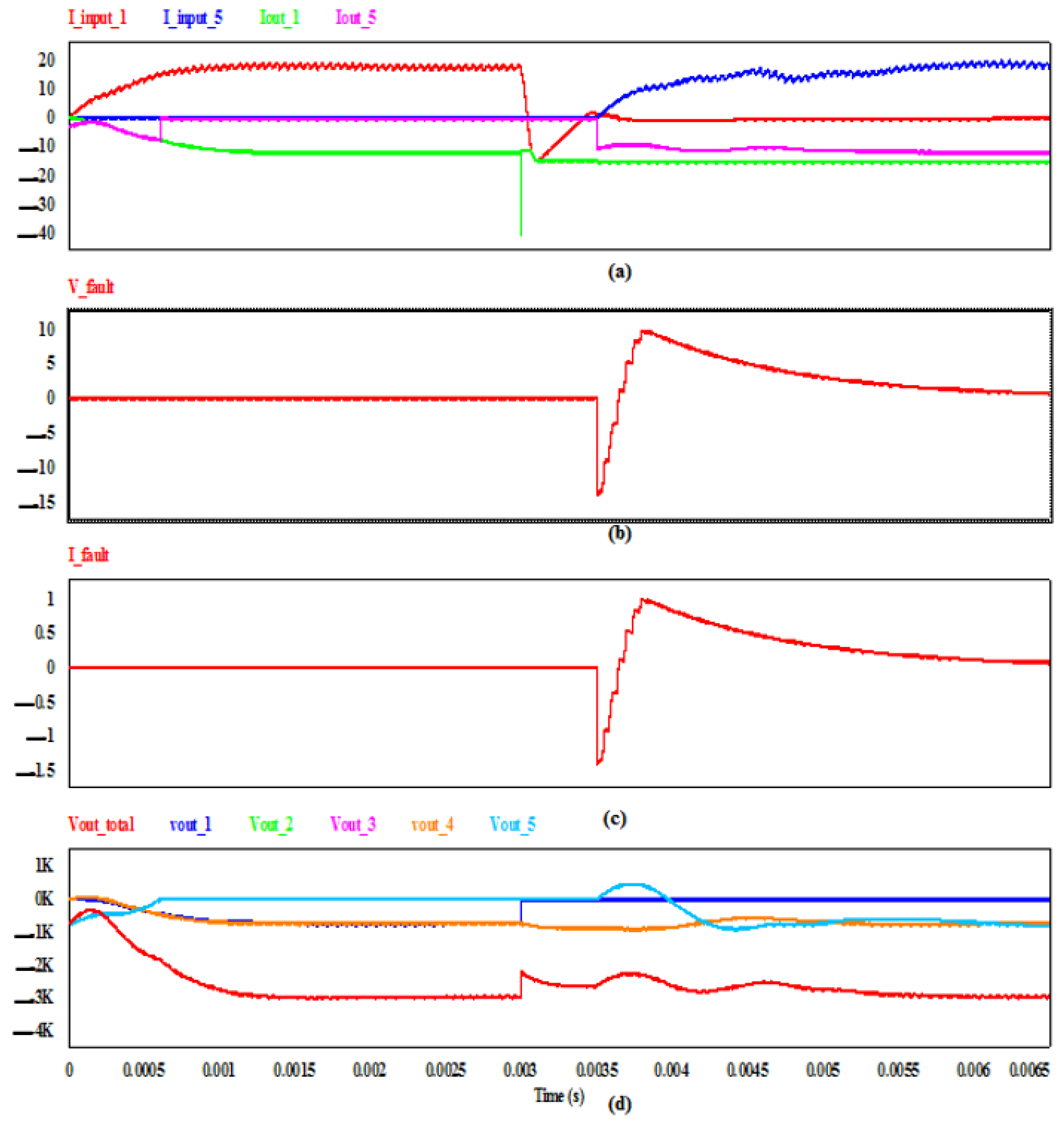
Figure 9.
The behavior of the converter during healthy and faulty conditions for case 2: (a) input and output currents (b) the faulty voltage (c) the faulty current and (d) output voltages and total output voltages.
Figure 9.
The behavior of the converter during healthy and faulty conditions for case 2: (a) input and output currents (b) the faulty voltage (c) the faulty current and (d) output voltages and total output voltages.
Figure 10.
The behavior of the converter during healthy and faulty conditions for case 3: (a) input and output currents (b) the faulty voltage (c) the faulty current and (d) output voltages and total output voltages.
Figure 10.
The behavior of the converter during healthy and faulty conditions for case 3: (a) input and output currents (b) the faulty voltage (c) the faulty current and (d) output voltages and total output voltages.
Figure 11.
The behavior of the converter during healthy and faulty conditions for case 4: (a) input and output currents (b) the faulty voltage (c) the faulty current and (d) output voltages and total output voltages.
Figure 11.
The behavior of the converter during healthy and faulty conditions for case 4: (a) input and output currents (b) the faulty voltage (c) the faulty current and (d) output voltages and total output voltages.
Figure 12.
The behavior of the converter during healthy and faulty conditions for case 5: (a) input and output currents (b) the faulty voltage (c) the faulty current and (d) output voltages and total output voltages.
Figure 12.
The behavior of the converter during healthy and faulty conditions for case 5: (a) input and output currents (b) the faulty voltage (c) the faulty current and (d) output voltages and total output voltages.
Figure 13.
The behavior of the converter during healthy and faulty conditions for case 6: (a) input and output currents (b) the faulty voltage (c) the faulty current and (d) output voltages and total output voltages.
Figure 13.
The behavior of the converter during healthy and faulty conditions for case 6: (a) input and output currents (b) the faulty voltage (c) the faulty current and (d) output voltages and total output voltages.
4. Simulation Results of the Fault Scenarios
To validate the fault tolerance of the proposed topology in
Figure 4, simulations were conducted using PSIM 11.1 software, incorporating an advanced control algorithm with advanced control as illustrated in
Figure 5. The parameters for the simulation are listed in
Table 2. Six fault scenarios were considered, each potentially occurring in various power modules. These scenarios include the following:
Open-circuit fault in switch S1
Open-circuit fault in switch S2
Open-circuit fault in switches S1/S2
Short-circuit fault in switch S1
Short-circuit fault in switch S2
Short-circuit fault in switches S1/S2
Figure 6,
Figure 9,
Figure 10,
Figure 11,
Figure 12 and
Figure 13 depict the dynamic response of the converter shown in
Figure 4 under four distinct operating conditions. From 0 to 3.0 ms, the system operates under healthy operation. Between 3.0 ms and 3.5 ms, a fault occurred. From 3.5 ms to 4.0 ms, the system undergoes fault recovery. After 4.0 ms, the system transitions into a fault-tolerant mode and resumes normal operation despite the presence of an open-circuit/short-circuit fault.
Table 2.
Specifications of the simulated system.
Table 2.
Specifications of the simulated system.
| Parameters | Values |
|---|
| Link capacitance in each power module | 3.125 µF |
| Link inductor | 150 µH |
| Input Voltage (Vi) | 500 V |
| Output voltage of each power module (Vo) | 750 V |
| Total Power | 3 kW |
| Number of power modules | 4 |
Case 1: Open-Circuit Fault in Switch S1:
When an open-circuit fault occurs in switch S1, the first power module is unable to deliver the required output voltage of 750 V. To address this, the system activates a backup power module by turning on switch Se_1, connecting it to the modular converter. Simultaneously, switch Sa_2 is activated, and Sa_1 is deactivated to release the remaining energy stored in the faulty power module. This release can be observed in the faulty voltage and current profiles in
Figure 6b and
Figure 6c, respectively. Switch Sa_3 is then turned on to isolate the faulty power module. Finally, switch Se_3 is turned off, allowing the backup module to take over, ensuring uninterrupted operation of the modular converter.
Figure 6a illustrates the input and output currents of both the primary and backup power modules during normal operation, fault occurrence, and the fault-tolerant state. Under healthy conditions, the input and output currents of the first power module are 16.8 A and 11.2 A, respectively. Following the fault, these values drop to zero, while the backup module’s currents rise from zero to 16.8 A and 11.2 A, respectively. As shown, once the backup module is activated and the faulty module isolated, the system resumes normal operation.
Figure 6d confirms that the total output voltage remains stable at 3000 V during both healthy and fault-tolerant operation. Additional simulation results are provided in
Figure 6,
Figure 7 and
Figure 8, offering detailed insights into the converter’s performance: (a) input and output currents of both the first and last power modules, (b) the release voltage of the faulty power module, (c) the release current of the faulty power module, and (d) the overall output voltage of the modular system and the individual output voltages of each power module.
Figure 7 and
Figure 8 further elaborate on this behavior.
Figure 7 shows the link voltages and currents during the fault for both the faulty and healthy power modules, while
Figure 8 displays the voltage and current profiles across the switches Sa_1, Sa_2, Sa_3, Se_1, and Se_3 during the fault recovery process.
2-Open-Circuit Fault in Switch S2:
When an open-circuit fault occurs in switch S2, the first power module becomes unable to generate the required output voltage of 750 V. In response, the backup power module is activated, with switch Se_1 turning on to connect this module to the converter. To discharge the remaining energy from the faulty first power module, switch Sa_2 is turned on, while Sa_1 is turned off. This energy release is reflected in the voltage and current fault waveforms shown in
Figure 9b and
Figure 9c, respectively. Additionally, switch Sa_3 activates to isolate the faulty power module. At the same time, switch Se_3 is turned off, allowing the output of the backup module to connect to the system, while the other power modules in the converter continue to function normally, as illustrated in
Figure 9d.
Figure 9a presents the input and output currents of both the first and backup power modules during normal operation, fault occurrence, and the fault-tolerant state. Under normal conditions, the input and output currents of the first power module are 16.8 A and 11.2 A, respectively. Once the fault occurs, these values drop to zero, while the backup power module takes over, with its input and output currents increasing to 16.8 A and 11.2 A, respectively. After the backup power module is fully integrated and the faulty first module is isolated, the modular converter resumes normal operation. As shown in
Figure 9d, the total output voltage remains at the expected 3000 V during both healthy operation and the fault-tolerant state.
3-Open-Circuit Fault in Switches S1/S2:
While it is rare for open-circuit faults to occur simultaneously in both switches S1 and S2, this scenario tests the robustness of the fault-tolerance mechanism. When an open-circuit fault arises in either switch S1 or S2, the first power module is unable to supply the required 750 V output. In response, the system activates the backup power module by turning on switch Se_1, connecting it to the converter. To safely discharge the residual energy from the faulty first power module, switch Sa_2 is turned on, and Sa_1 is turned off. This energy release is visible in the voltage and current fault graphs, as shown in
Figure 10b,c. Next, switch Sa_3 is engaged to fully isolate the defective power module. At the same time, switch Se_3 is turned off to allow the backup module’s output to feed into the system while all other power modules continue to operate normally, as depicted in
Figure 10d.
Figure 10a illustrates the input and output currents of both the first and backup power modules during normal operation, fault occurrence, and the fault-tolerant state. Under normal conditions, the input and output currents of the first power module are 16.8 A and 11.2 A, respectively. When the fault occurs, these values drop to zero, and the backup power module takes over, with its input and output currents increasing to 16.8 A and 11.2 A from zero. Once the backup module is fully integrated and the faulty first module is isolated, the converter returns to normal operation.
Figure 10d shows that the total output voltage remains at the expected 3000 V during both healthy and fault-tolerant conditions, ensuring stable performance throughout.
4-Short-Circuit Fault in Switch S1:
When a short-circuit fault occurs in switch S1, the first power module loses its ability to generate the required output voltage of 750 V. In response, the system activates the backup power module by turning on switch Se_1, connecting it to the converter. To safely discharge the remaining energy in the faulty first power module, switch Sa_2 is turned on, while Sa_1 is turned off. This discharge process is visible in the voltage and current fault patterns shown in
Figure 11b,c. Additionally, switch Sa_3 is engaged to fully isolate the defective power module. Meanwhile, switch Se_3 is turned off, allowing the backup module’s output to integrate with the converter while the other modules continue to function normally, as demonstrated in
Figure 11d.
Figure 11a highlights the input and output currents of both the first and backup power modules during normal operation, fault occurrence, and fault-tolerant states. Under normal conditions, the first power module has input and output currents of 16.8 A and 11.2 A, respectively. When the fault occurs, these values drop to zero, while the backup power module steps in, with its input and output currents rising from zero to 16.8 A and 11.2 A, respectively. Once the backup module is fully engaged and the faulty first module is isolated, the modular converter resumes normal operation.
Figure 11d shows that the total output voltage remains at the expected 3000 V during both healthy operation and the fault-tolerant state, ensuring continuous and reliable system performance.
5-Short-Circuit Fault in Switch S2:
When a short-circuit fault occurs in switch S2, the first power module becomes unable to generate the required output voltage of 750 V. In this scenario, the backup power module takes over, and switch Se_1 is activated to connect the backup module to the system. To safely discharge the remaining energy stored in the faulty first power module, switch Sa_2 is turned on and switch Sa_1 is turned off. This energy release is reflected in the voltage and current voltage fault patterns shown in
Figure 12b,c. To fully isolate the malfunctioning module, switch Sa_3 is engaged. Meanwhile, switch Se_3 is turned off to enable the backup power module to connect its output to the converter, ensuring uninterrupted operation of the remaining power modules, as shown in
Figure 12d.
Figure 12a illustrates the input and output currents of both the first and backup power modules during normal operation, fault occurrence, and the fault-tolerant state. Under normal conditions, the input and output currents of the first power module are 16.8 A and 11.2 A, respectively. When the fault occurs, these currents drop to zero, while the backup module’s input and output currents rise to 16.8 A and 11.2 A, respectively, from their previous values of zero. Once the backup module is successfully integrated and the faulty first module is isolated, the converter resumes normal operation. As depicted in
Figure 12d, the total output voltage remains stable at 3000 V, both during healthy operation and in the fault-tolerant state, ensuring seamless system performance throughout
6-Short-Circuit Fault in Switches S1/S2:
Although short-circuit faults occurring simultaneously in both switches S1 and S2 are rare, this scenario is designed to test the robustness of the fault-tolerance method. When such a fault occurs, the first power module is unable to produce the required 750 V output. In this case, the system responds by activating the backup power module, turning on switch Se_1 to connect it to the converter. To safely discharge the remaining energy in the faulty first power module, switch Sa_2 is turned on while Sa_1 is turned off. This energy release is captured in the current and voltage fault patterns shown in
Figure 13b,c. Additionally, switch Sa_3 is engaged to isolate the faulty module. At the same time, switch Se_3 is turned off to connect the backup power module’s output to the converter, allowing the other power modules to continue operating without disruption, as shown in
Figure 13d.
Figure 13a illustrates the input and output currents of both the first and backup power modules during normal operation, fault occurrence, and the fault-tolerant state. During healthy operation, the first power module operates with input and output currents of 16.8 A and 11.2 A, respectively. However, after the fault occurs, these values drop to zero, while the backup module takes over, increasing its input and output currents from zero to 16.8 A and 11.2 A, respectively. Once the backup power module is fully integrated and the faulty first module is isolated, the modular converter resumes normal operation.
Figure 13d confirms that the total output voltage remains stable at 3000 V, both under healthy conditions and in the fault-tolerant mode, ensuring reliable and continuous performance.
6. Discussion and Analysis
The proposed fault-tolerant design incurs a 22% increase in switch count compared to non-redundant designs but remains 35–40% more cost-effective than full-bridge SM (FBSM) solutions [
33,
34,
35,
36] that require four switches per module. The backup module adds 20% to the base cost, but this is offset by a 60% reduction in downtime-related losses (estimated at
$15 k/hour for HVDC applications [
12].
Table 4 introduces the comparison of cost and performance metrics with existing techniques:
Compared to full-bridge SMs [
33,
34,
35,
36], the proposed method reduces switch count by 35% (three vs. four switches/module) while achieving comparable fault recovery times (0.5 ms vs. 0.3 ms). Cold-reserve solutions [
26,
27] exhibit 2.1 ms recovery but lack real-time reconfiguration. Hybrid breakers [
29,
30] offer faster isolation (0.1 ms) but at 70% higher cost. While the proposed design incurs a 22% higher initial cost than non-redundant topologies, The total cost of is 15% lower, achieved through an 80% reduction in maintenance costs (fewer module replacements), 30% longer mean time between failures (MTBFs), and 50% faster fault recovery, minimizing revenue losses in critical applications like HVDC and renewable energy systems. This cost–reliability balance positions it as a viable alternative to conventional fault-tolerant methods (e.g., full-bridge SMs or hybrid breakers) in high-availability scenarios. The design optimizes cost–reliability trade-offs by employing the following: (1) partial redundancy (one backup module per N active modules) rather than 1:1 redundancy, (2) standard half-bridge switches instead of specialized components (e.g., clamp-diode or full-bridge SMs), and (3) localized fault management to minimize control complexity. This approach reduces hardware overhead while maintaining 99.98% system availability, as shown in the simulation results.
The initial efficiency estimate of >98% accounts for conduction losses in all semiconductors and components during steady-state operation. A complete energy balance must also consider switching and transient recovery losses. The main power switches (S1, S2) achieve high efficiency through zero-current switching (ZCS) turn-off and soft turn-on, minimizing their switching losses. The primary additional losses are as follows: (1) conduction losses from the always-on supplementary switches (e.g., Sa_1); (2) hard-switching losses incurred by the supplementary switches (Sa_2, Sa_3, Se_1) during the rare fault recovery events, which are a transient phenomenon with negligible average power impact but must be considered for SOA; and (3) the intentional dissipation of energy stored in a faulty module’s link capacitor during the isolation process. A detailed quantitative breakdown of these loss components, including core losses in the magnetic elements, will be a key focus of future experimental validation on a physical prototype.
The proposed fault-tolerant architecture becomes increasingly advantageous as the number of modules, N, scales up for higher-power applications. Quantitative analysis reveals that the hardware redundancy overhead decreases significantly, with the switch count per functional power module converging from 6.25 (N = 4) to 5.25 (N = 20). Furthermore, the relative voltage dip during a fault scales inversely with N, projected to be below 0.3% for a 20-module system, enhancing inherent output stability. The system-level efficiency impact of the fault-tolerant circuitry diminishes as the fixed loss of the backup path is amortized over more active modules. Critically, the control complexity does not adversely evolve; the centralized FPGA-based algorithm maintains deterministic, sub-millisecond fault recovery by processing all modules in parallel, with the scaling challenge confined to manageable I/O expansion rather than increased logical latency. It is also acknowledged that the centralized control architecture necessitates high-speed data acquisition from all modules, which imposes a constant data transmission load. Future iterations of the control system could explore hybrid architectures, such as incorporating event-triggered mechanisms [
50], to alleviate this communication burden for non-critical monitoring tasks, while preserving the deterministic, high-frequency sampling required for the core fault detection loop.

